The world is witnessing an unprecedented surge in semiconductor manufacturing investments, a direct response to the insatiable demand for Artificial Intelligence (AI) chips. As of November 2025, governments and leading tech giants are funneling hundreds of billions of dollars into new fabrication facilities (fabs), advanced memory production, and cutting-edge research and development. This global chip race is not merely about increasing capacity; it's a strategic imperative to secure the future of AI, promising to reshape the technological landscape and redefine geopolitical power dynamics. The immediate significance for the AI industry is profound, guaranteeing a more robust and resilient supply chain for the high-performance silicon that powers everything from generative AI models to autonomous systems.
This monumental investment wave aims to alleviate bottlenecks, accelerate innovation, and decentralize a historically concentrated supply chain. The initiatives are poised to triple chipmaking capacity in key regions, ensuring that the exponential growth of AI applications can be met with equally rapid advancements in underlying hardware.
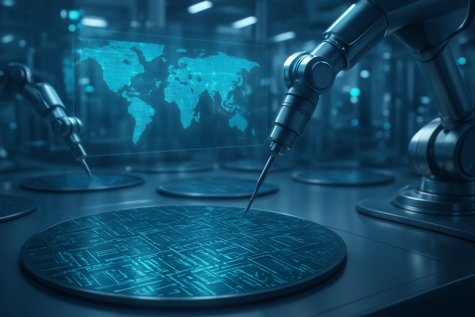
Engineering Tomorrow: The Technical Heart of the Semiconductor Boom
The current wave of investment is characterized by a relentless pursuit of the most advanced manufacturing nodes and memory technologies crucial for AI. Taiwan Semiconductor Manufacturing Company (TSMC) (NYSE: TSM), the world's largest contract chipmaker, is leading the charge with a staggering $165 billion planned investment in the United States, including three new fabrication plants, two advanced packaging facilities, and a major R&D center in Arizona. These facilities are slated to produce highly advanced chips using 2nm and 1.6nm processes, with initial production expected in early 2025 and 2028. Globally, TSMC plans to build and equip nine new production facilities in 2025, focusing on these leading-edge nodes across Taiwan, the U.S., Japan, and Germany. A critical aspect of TSMC's strategy is investment in backend processing in Taiwan, addressing a key bottleneck for AI chip output.
Memory powerhouses are equally aggressive. SK Hynix is committing approximately $74.5 billion between 2024 and 2028, with 80% directed towards AI-related areas like High Bandwidth Memory (HBM) production. The company has already sold out of its HBM chips for 2024 and most of 2025, largely driven by demand from Nvidia's (NASDAQ: NVDA) GPU accelerators. A $3.87 billion HBM memory packaging plant and R&D facility in West Lafayette, Indiana, supported by the U.S. CHIPS Program Office, is set for mass production by late 2028. Meanwhile, their M15X fab in South Korea, a $14.7 billion investment, is set to begin mass production of next-generation DRAM, including HBM2, by November 2025, with plans to double HBM production year-over-year. Similarly, Samsung (KRX: 005930) is pouring hundreds of billions into its semiconductor division, including a $17 billion fabrication plant in Taylor, Texas, expected to open in late 2024 and focusing on 3-nanometer (nm) semiconductors, with an expected doubling of investment to $44 billion. Samsung is also reportedly considering a $7 billion U.S. advanced packaging plant for HBM. Micron Technology (NASDAQ: MU) is increasing its capital expenditure to $8.1 billion in fiscal year 2025, primarily for HBM investments, with its HBM for AI applications already sold out for 2024 and much of 2025. Micron aims for a 20-25% HBM market share by 2026, supported by a new packaging facility in Singapore.
These investments mark a significant departure from previous approaches, particularly with the widespread adoption of Gate-All-Around (GAA) transistor architecture in 2nm and 1.6nm processes by Intel, Samsung, and TSMC. GAA offers superior gate control and reduced leakage compared to FinFET, enabling more powerful and energy-efficient AI processors. The emphasis on advanced packaging, like TSMC's U.S. investments and SK Hynix's Indiana plant, is also crucial, as it allows for denser integration of logic and memory, directly boosting the performance of AI accelerators. Initial reactions from the AI research community and industry experts highlight the critical need for this expanded capacity and advanced technology, calling it essential for sustaining the rapid pace of AI innovation and preventing future compute bottlenecks.
Reshaping the AI Competitive Landscape
The massive investments in semiconductor manufacturing are set to profoundly impact AI companies, tech giants, and startups alike, creating both significant opportunities and competitive pressures. Companies at the forefront of AI development, particularly those designing their own custom AI chips or heavily reliant on high-performance GPUs, stand to benefit immensely from the increased supply and technological advancements.
Nvidia (NASDAQ: NVDA), a dominant force in AI hardware, will see its supply chain for crucial HBM chips strengthened, enabling it to continue delivering its highly sought-after GPU accelerators. The fact that SK Hynix and Micron's HBM is sold out for years underscores the demand, and these expansions are critical for future Nvidia product lines. Tesla (NASDAQ: TSLA) is reportedly exploring partnerships with Intel's (NASDAQ: INTC) foundry operations to secure additional manufacturing capacity for its custom AI chips, indicating the strategic importance of diverse sourcing. Similarly, Amazon Web Services (AWS) (NASDAQ: AMZN) has committed to a multiyear, multibillion-dollar deal with Intel for new custom Intel® Xeon® 6 and AI fabric chips, showcasing the trend of tech giants leveraging foundry services for tailored AI solutions.
For major AI labs and tech companies, access to cutting-edge 2nm and 1.6nm chips and abundant HBM will be a significant competitive advantage. Those who can secure early access or have captive manufacturing capabilities (like Samsung) will be better positioned to develop and deploy next-generation AI models. This could potentially disrupt existing product cycles, as new hardware enables capabilities previously impossible, accelerating the obsolescence of older AI accelerators. Startups, while benefiting from a broader supply, may face challenges in competing for allocation of the most advanced, highest-demand chips against larger, more established players. The strategic advantage lies in securing robust supply chains and leveraging these advanced chips to deliver groundbreaking AI products and services, further solidifying market positioning for the well-resourced.
A New Era for Global AI
These unprecedented investments fit squarely into the broader AI landscape as a foundational pillar for its continued expansion and maturation. The "AI boom," characterized by the proliferation of generative AI and large language models, has created an insatiable demand for computational power. The current fab expansions and government initiatives are a direct and necessary response to ensure that the hardware infrastructure can keep pace with the software innovation. This push for localized and diversified semiconductor manufacturing also addresses critical geopolitical concerns, aiming to reduce reliance on single regions and enhance national security by securing the supply chain for these strategic components.
The impacts are wide-ranging. Economically, these investments are creating hundreds of thousands of high-tech manufacturing and construction jobs globally, stimulating significant economic growth in regions like Arizona, Texas, and various parts of Asia. Technologically, they are accelerating innovation beyond just chip production; AI is increasingly being used in chip design and manufacturing processes, reducing design cycles by up to 75% and improving quality. This virtuous cycle of AI enabling better chips, which in turn enable better AI, is a significant trend. Potential concerns, however, include the immense capital expenditure required, the global competition for skilled talent to staff these advanced fabs, and the environmental impact of increased manufacturing. Comparisons to previous AI milestones, such as the rise of deep learning or the advent of transformers, highlight that while software breakthroughs capture headlines, hardware infrastructure investments like these are equally, if not more, critical for turning theoretical potential into widespread reality.
The Road Ahead: What's Next for AI Silicon
Looking ahead, the near-term will see the ramp-up of 2nm and 1.6nm process technologies, with initial production from TSMC and Intel's 18A process expected to become more widely available through 2025. This will unlock new levels of performance and energy efficiency for AI accelerators, enabling larger and more complex AI models to run more effectively. Further advancements in HBM, such as SK Hynix's HBM4 later in 2025, will continue to address the memory bandwidth bottleneck, which is critical for feeding the massive datasets used by modern AI.
Long-term developments include the continued exploration of novel chip architectures like neuromorphic computing and advanced heterogeneous integration, where different types of processing units (CPUs, GPUs, AI accelerators) are tightly integrated on a single package. These will be crucial for specialized AI workloads and edge AI applications. Potential applications on the horizon include more sophisticated real-time AI in autonomous vehicles, hyper-personalized AI assistants, and increasingly complex scientific simulations. Challenges that need to be addressed include sustaining the massive funding required for future process nodes, attracting and retaining a highly specialized workforce, and overcoming the inherent complexities of manufacturing at atomic scales. Experts predict a continued acceleration in the symbiotic relationship between AI software and hardware, with AI playing an ever-greater role in optimizing chip design and manufacturing, leading to a new era of AI-driven silicon innovation.
A Foundational Shift for the AI Age
The current wave of investments in semiconductor manufacturing represents a foundational shift, underscoring the critical role of hardware in the AI revolution. The billions poured into new fabs, advanced memory production, and government initiatives are not just about meeting current demand; they are a strategic bet on the future, ensuring the necessary infrastructure exists for AI to continue its exponential growth. Key takeaways include the unprecedented scale of private and public investment, the focus on cutting-edge process nodes (2nm, 1.6nm) and HBM, and the strategic imperative to diversify global supply chains.
This development's significance in AI history cannot be overstated. It marks a period where the industry recognizes that software breakthroughs, while vital, are ultimately constrained by the underlying hardware. By building out this robust manufacturing capability, the industry is laying the groundwork for the next generation of AI applications, from truly intelligent agents to widespread autonomous systems. What to watch for in the coming weeks and months includes the progress of initial production at these new fabs, further announcements regarding government funding and incentives, and how major AI companies leverage this increased compute power to push the boundaries of what AI can achieve. The future of AI is being forged in silicon, and the investments made today will determine the pace and direction of its evolution for decades to come.
This content is intended for informational purposes only and represents analysis of current AI developments.
TokenRing AI delivers enterprise-grade solutions for multi-agent AI workflow orchestration, AI-powered development tools, and seamless remote collaboration platforms.
For more information, visit https://www.tokenring.ai/.