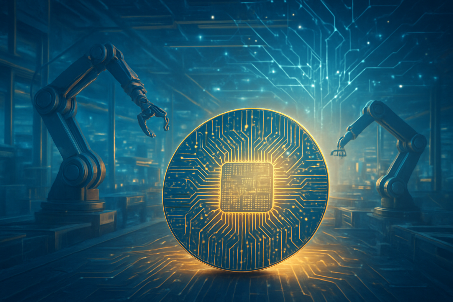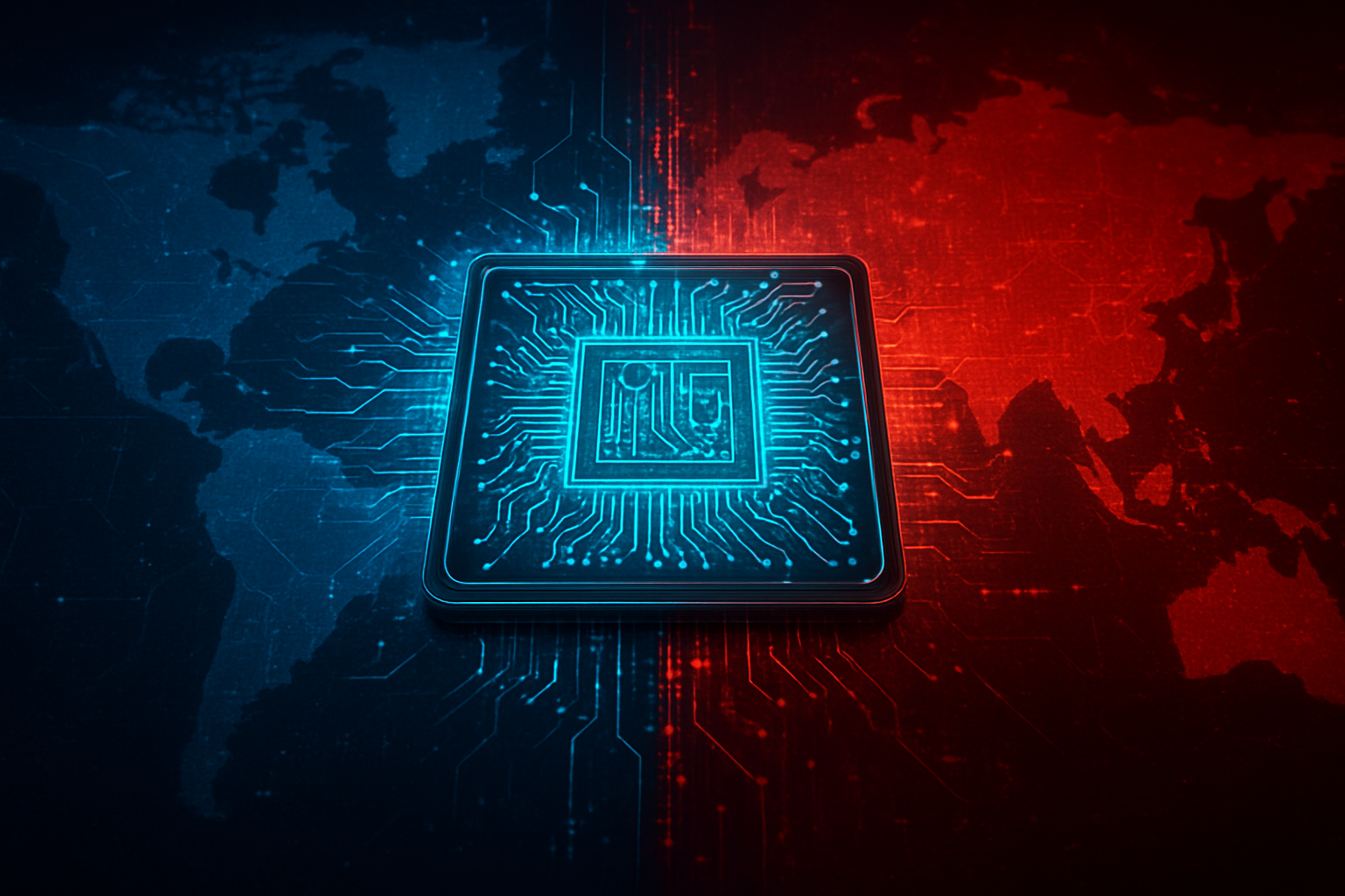
November 2025 marks an unprecedented surge in AI chip innovation, characterized by the commercialization of brain-like computing, a leap into light-speed processing, and a manufacturing paradigm shift towards modularity and AI-driven efficiency. These breakthroughs are immediately reshaping the technological landscape, driving sustainable, powerful AI from the cloud to the farthest edge of the network.
The artificial intelligence hardware sector is currently undergoing a profound transformation, with significant advancements in both chip design and manufacturing processes directly addressing the escalating demands for performance, energy efficiency, and scalability. The immediate significance of these developments lies in their capacity to accelerate AI deployment across industries, drastically reduce its environmental footprint, and enable a new generation of intelligent applications that were previously out of reach due to computational or power constraints.
Technical Deep Dive: The Engines of Tomorrow's AI
The core of this revolution lies in several distinct yet interconnected technical advancements. Neuromorphic computing, which mimics the human brain's neural architecture, is finally moving beyond theoretical research into practical, commercial applications. Chips like Intel's (NASDAQ: INTC) Hala Point system, BrainChip's (ASX: BRN) Akida Pulsar, and Innatera's Spiking Neural Processor (SNP), have seen significant advancements or commercial launches in 2025. These systems are inherently energy-efficient, offering low-latency solutions ideal for edge AI, robotics, and the Internet of Things (IoT). For instance, Akida Pulsar boasts up to 500 times lower energy consumption and 100 times latency reduction compared to conventional AI cores for real-time, event-driven processing at the edge. Furthermore, USC researchers have demonstrated artificial neurons that replicate biological function with significantly reduced chip size and energy consumption, promising to advance artificial general intelligence. This paradigm shift directly addresses the critical need for sustainable AI by drastically cutting power usage in resource-constrained environments.
Another major bottleneck in traditional computing architectures, the "memory wall," is being shattered by in-memory computing (IMC) and processing-in-memory (PIM) chips. These innovative designs perform computations directly within memory, dramatically reducing the movement of data between the processor and memory. This reduction in data transfer, in turn, slashes power consumption and significantly boosts processing speed. Companies like Qualcomm (NASDAQ: QCOM) are integrating near-memory computing into new solutions such as the AI250, providing a generational leap in effective memory bandwidth and efficiency specifically for AI inference workloads. This technology is crucial for managing the massive data processing demands of complex AI algorithms, enabling faster and more efficient training and inference for burgeoning generative AI models and large language models (LLMs).
Perhaps one of the most futuristic developments is the emergence of optical computing. Scientists at Tsinghua University have achieved a significant milestone by developing a light-powered AI chip, OFE², capable of handling data at an unprecedented 12.5 GHz. This optical computing breakthrough completes complex pattern-recognition tasks by directing light beams through on-chip structures, consuming significantly less energy than traditional electronic devices. This innovation offers a potent solution to the growing energy demands of AI, potentially freeing AI from being a major contributor to global energy shortages. It promises a new generation of real-time, ultra-low-energy AI, crucial for sustainable and widespread deployment across various sectors.
Finally, as traditional transistor scaling (often referred to as Moore's Law) faces physical limits, advanced packaging technologies and chiplet architectures have become paramount. Technologies like 2.5D and 3D stacking (e.g., CoWoS, 3DIC), Fan-Out Panel-Level Packaging (FO-PLP), and hybrid bonding are crucial for boosting performance, increasing integration density, improving signal integrity, and enhancing thermal management for AI chips. Complementing this, chiplet technology, which involves modularizing chip functions into discrete components, is gaining significant traction, with the Universal Chiplet Interconnect Express (UCIe) standard expanding its adoption. These innovations are the new frontier for hardware optimization, offering flexibility, cost-effectiveness, and faster development cycles. They also mitigate supply chain risks by allowing manufacturers to source different parts from multiple suppliers. The market for advanced packaging is projected to grow eightfold by 2033, underscoring its immediate importance for the widespread adoption of AI chips into consumer devices and automotive applications.
Competitive Landscape: Winners and Disruptors
These advancements are creating clear winners and potential disruptors within the AI industry. Chip designers and manufacturers at the forefront of these innovations stand to benefit immensely. Intel, with its neuromorphic Hala Point system, and BrainChip, with its Akida Pulsar, are well-positioned in the energy-efficient edge AI market. Qualcomm's integration of near-memory computing in its AI250 strengthens its leadership in mobile and edge AI processing. NVIDIA (NASDAQ: NVDA), while not explicitly mentioned for neuromorphic or optical chips, continues to dominate the high-performance computing space for AI training and is a key enabler for AI-driven manufacturing.
The competitive implications are significant. Major AI labs and tech companies reliant on traditional architectures will face pressure to adapt or risk falling behind in performance and energy efficiency. Companies that can rapidly integrate these new chip designs into their products and services will gain a substantial strategic advantage. For instance, the ability to deploy AI models with significantly lower power consumption opens up new markets in battery-powered devices, remote sensing, and pervasive AI. The modularity offered by chiplets could also democratize chip design to some extent, allowing smaller players to combine specialized chiplets from various vendors to create custom, high-performance AI solutions, potentially disrupting the vertically integrated chip design model.
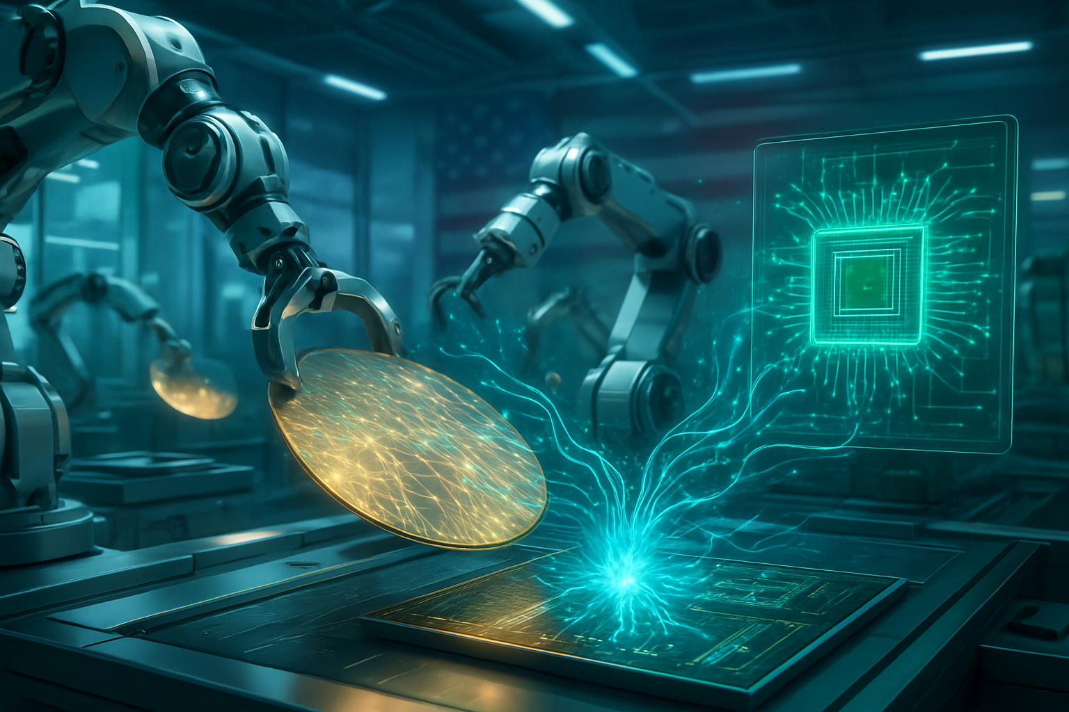
Furthermore, AI's role in optimizing its own creation is a game-changer. AI-driven Electronic Design Automation (EDA) tools are dramatically accelerating chip design timelines—for example, reducing a 5nm chip's optimization cycle from six months to just six weeks. This means faster time-to-market for new AI chips, improved design quality, and more efficient, higher-yield manufacturing processes. Samsung (KRX: 005930), for instance, is establishing an "AI Megafactory" powered by 50,000 NVIDIA GPUs to revolutionize its chip production, integrating AI throughout its entire manufacturing flow. Similarly, SK Group is building an "AI factory" in South Korea with NVIDIA, focusing on next-generation memory and autonomous fab digital twins to optimize efficiency. These efforts are critical for meeting the skyrocketing demand for AI-optimized semiconductors and bolstering supply chain resilience amidst geopolitical shifts.
Broader Significance: Shaping the AI Future
These innovations fit perfectly into the broader AI landscape, addressing critical trends such as the insatiable demand for computational power for increasingly complex models (like LLMs), the push for sustainable and energy-efficient AI, and the proliferation of AI at the edge. The move towards neuromorphic and optical computing represents a fundamental shift away from the Von Neumann architecture, which has dominated computing for decades, towards more biologically inspired or physically optimized processing methods. This transition is not merely an incremental improvement but a foundational change that could unlock new capabilities in AI.
The impacts are far-reaching. On one hand, these advancements promise more powerful, ubiquitous, and efficient AI, enabling breakthroughs in areas like personalized medicine, autonomous systems, and advanced scientific research. On the other hand, potential concerns, while mitigated by the focus on energy efficiency, still exist regarding the ethical implications of more powerful AI and the increasing complexity of hardware development. However, the current trajectory is largely positive, aiming to make AI more accessible and environmentally responsible.
Comparing this to previous AI milestones, such as the rise of GPUs for deep learning or the development of specialized AI accelerators like Google's TPUs, these current advancements represent a diversification and deepening of the hardware foundation. While earlier milestones focused on brute-force parallelization, today's innovations are about architectural efficiency, novel physics, and self-optimization through AI, pushing beyond the limits of traditional silicon. This multi-pronged approach suggests a more robust and sustainable path for AI's continued growth.
The Road Ahead: Future Developments and Challenges
Looking to the near-term, we can expect to see further integration of these technologies. Hybrid chips combining neuromorphic, in-memory, and conventional processing units will likely become more common, optimizing specific workloads for maximum efficiency. The UCIe standard for chiplets will continue to gain traction, leading to a more modular and customizable AI hardware ecosystem. In the long-term, the full potential of optical computing, particularly in areas requiring ultra-high bandwidth and low latency, could revolutionize data centers and telecommunications infrastructure, creating entirely new classes of AI applications.
Potential applications on the horizon include highly sophisticated, real-time edge AI for autonomous vehicles that can process vast sensor data with minimal latency and power, advanced robotics capable of learning and adapting in complex environments, and medical devices that can perform on-device diagnostics with unprecedented accuracy and speed. Generative AI and LLMs will also see significant performance boosts, enabling more complex and nuanced interactions, and potentially leading to more human-like AI capabilities.
However, challenges remain. Scaling these nascent technologies to mass production while maintaining cost-effectiveness is a significant hurdle. The development of robust software ecosystems and programming models that can fully leverage the unique architectures of neuromorphic and optical chips will be crucial. Furthermore, ensuring interoperability between diverse chiplet designs and maintaining supply chain stability amidst global economic fluctuations will require continued innovation and international collaboration. Experts predict a continued convergence of hardware and software co-design, with AI playing an ever-increasing role in optimizing its own underlying infrastructure.
A New Era for AI Hardware
In summary, the latest innovations in AI chip design and manufacturing—encompassing neuromorphic computing, in-memory processing, optical chips, advanced packaging, and AI-driven manufacturing—represent a pivotal moment in the history of artificial intelligence. These breakthroughs are not merely incremental improvements but fundamental shifts that promise to make AI more powerful, energy-efficient, and ubiquitous than ever before.
The significance of these developments cannot be overstated. They are addressing the core challenges of AI scalability and sustainability, paving the way for a future where AI is seamlessly integrated into every facet of our lives, from smart cities to personalized health. As we move forward, the interplay between novel chip architectures, advanced manufacturing techniques, and AI's self-optimizing capabilities will be critical to watch. The coming weeks and months will undoubtedly bring further announcements and demonstrations as companies race to capitalize on these transformative technologies, solidifying this period as a new era for AI hardware.
This content is intended for informational purposes only and represents analysis of current AI developments.
TokenRing AI delivers enterprise-grade solutions for multi-agent AI workflow orchestration, AI-powered development tools, and seamless remote collaboration platforms.
For more information, visit https://www.tokenring.ai/.