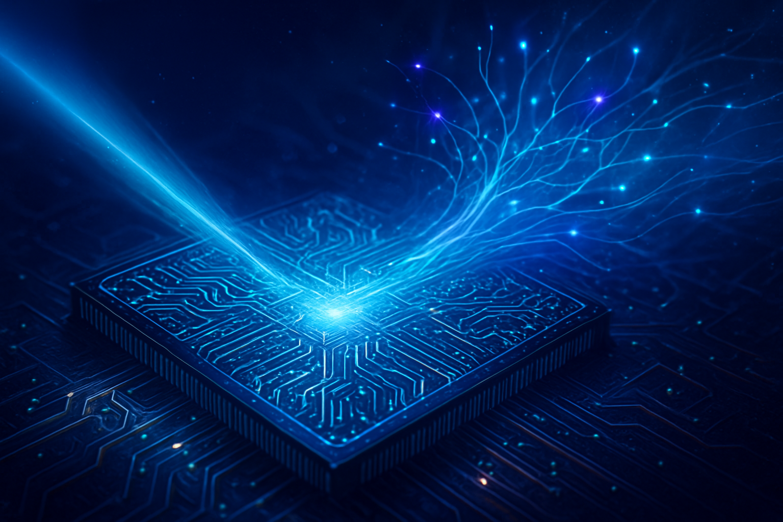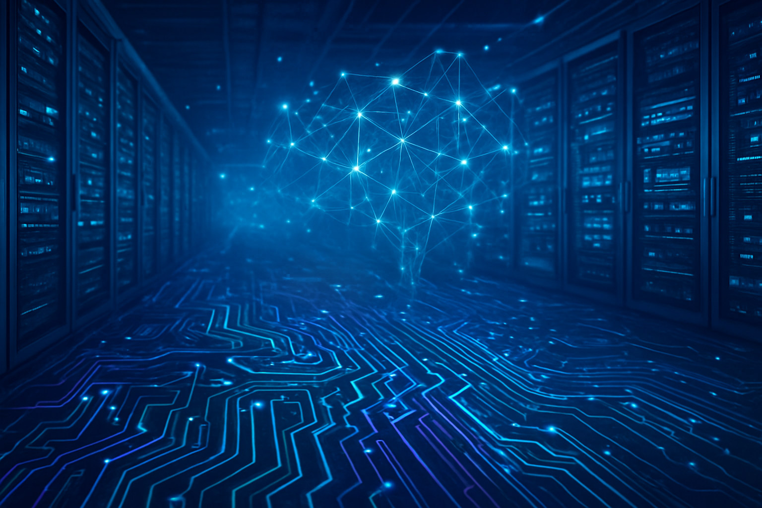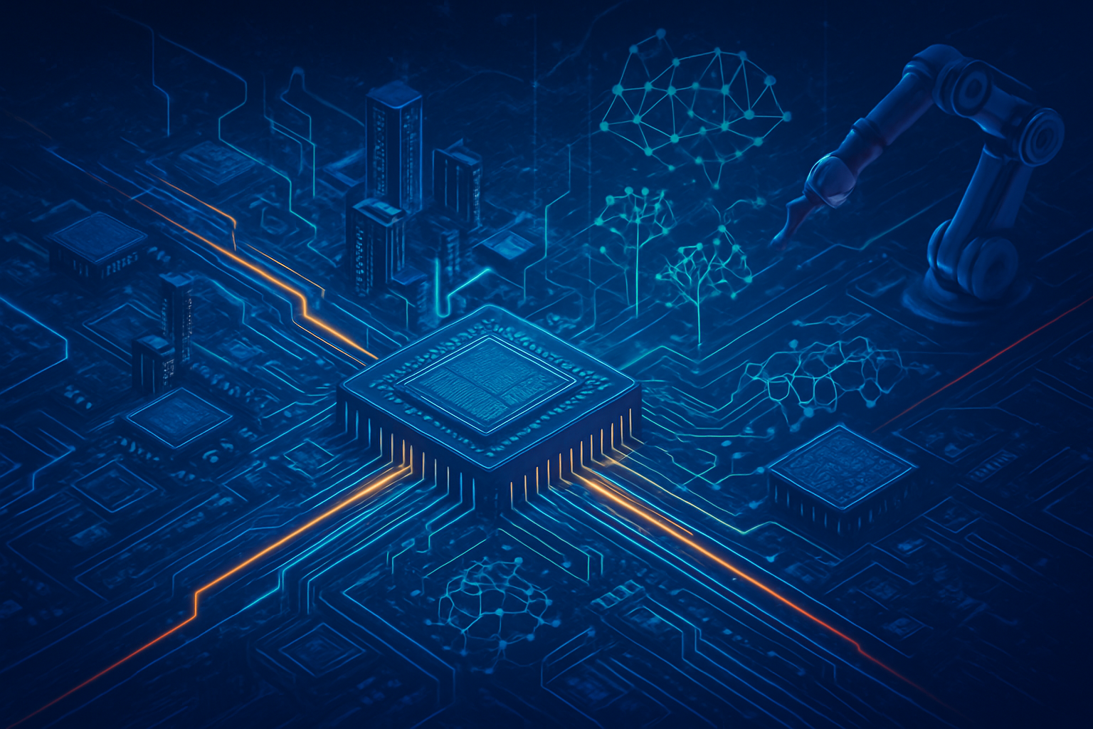
The relentless march of artificial intelligence, particularly the explosion of large language models (LLMs) and the proliferation of AI at the edge, has ushered in a new era where general-purpose processors can no longer keep pace. In late 2025, AI accelerators and specialized hardware have emerged as the indispensable bedrock, purpose-built to unleash unprecedented performance, efficiency, and scalability across the entire AI landscape. These highly optimized computing units are not just augmenting existing systems; they are fundamentally reshaping how AI models are trained, deployed, and experienced, driving a profound transformation that is both immediate and strategically critical.
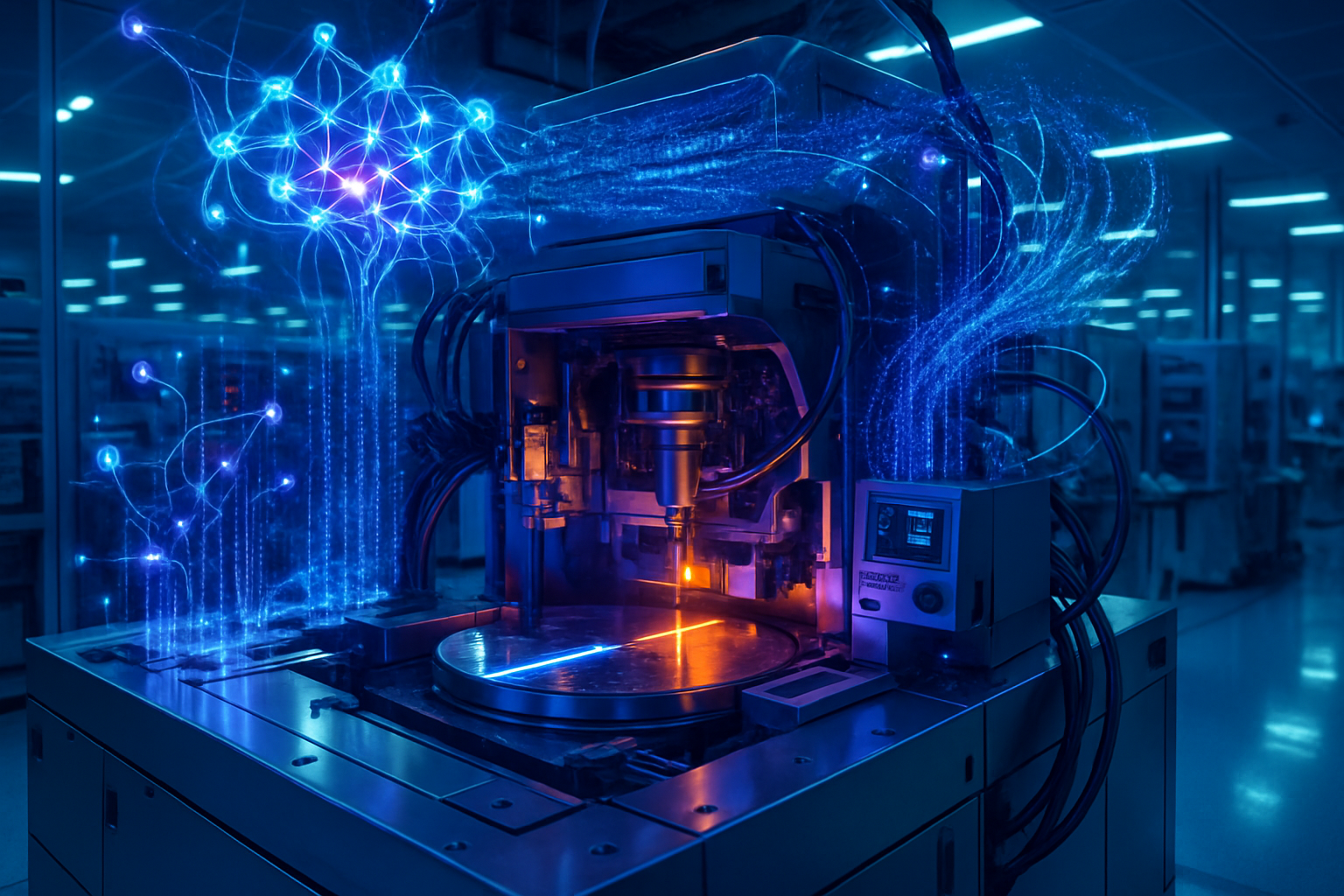
At their core, AI accelerators are specialized hardware devices, often taking the form of chips or entire computer systems, meticulously engineered to expedite artificial intelligence and machine learning applications. Unlike traditional Central Processing Units (CPUs) that operate sequentially, these accelerators are designed for the massive parallelism and complex mathematical computations—such as matrix multiplications—inherent in neural networks, deep learning, and computer vision tasks. This specialized design allows them to handle the intensive calculations demanded by modern AI models with significantly greater speed and efficiency, making real-time processing and analysis feasible in scenarios previously deemed impossible. Key examples include Graphics Processing Units (GPUs), Neural Processing Units (NPUs), Tensor Processing Units (TPUs), Field-Programmable Gate Arrays (FPGAs), and Application-Specific Integrated Circuits (ASICs), each offering distinct optimizations for AI workloads.
Their immediate significance in the current AI landscape (late 2025) is multifaceted and profound. Firstly, these accelerators provide the raw computational horsepower and energy efficiency crucial for training ever-larger and more complex AI models, particularly the demanding LLMs, which general-purpose hardware struggles to manage reliably. This enhanced capability translates directly into faster innovation cycles and the ability to explore more sophisticated AI architectures. Secondly, specialized hardware is pivotal for the burgeoning field of edge AI, enabling intelligent processing directly on devices like smartphones, autonomous vehicles, and IoT sensors with minimal latency, reduced reliance on cloud connectivity, and improved privacy. Companies are increasingly integrating NPUs and other AI-specific cores into consumer electronics to support on-device AI experiences. Thirdly, within cloud computing and hyperscale data centers, AI accelerators are essential for scaling the massive training and inference tasks that power sophisticated AI services, with major players like Google (NASDAQ: GOOGL) (TPUs) and Amazon (NASDAQ: AMZN) (Inferentia, Trainium) deploying their own specialized silicon. The global AI chip market is projected to exceed $150 billion in 2025, underscoring this dramatic shift towards specialized hardware as a critical differentiator. Furthermore, the drive for specialized AI hardware is also addressing the "energy crisis" of AI, offering significantly improved power efficiency over general-purpose processors, thereby reducing operational costs and making AI more sustainable. The industry is witnessing a rapid evolution towards heterogeneous computing, where various accelerators work in concert to optimize performance and efficiency, cementing their role as the indispensable engines powering the ongoing artificial intelligence revolution.
Specific Advancements and Technical Specifications
Leading manufacturers and innovative startups are pushing the boundaries of silicon design, integrating advanced process technologies, novel memory solutions, and specialized computational units.
Key Players and Their Innovations:
- NVIDIA (NASDAQ: NVDA): Continues to dominate the AI GPU market, with its Blackwell architecture (B100, B200) having ramped up production in early 2025. NVIDIA's roadmap extends to the next-generation Vera Rubin Superchip, comprising two Rubin GPUs and an 88-core Vera CPU, slated for mass production around Q3/Q4 2026, followed by Rubin Ultra in 2027. Blackwell GPUs are noted for being 50,000 times faster than the first CUDA GPU, emphasizing significant gains in speed and scale.
- Intel (NASDAQ: INTC): Is expanding its AI accelerator portfolio with the Gaudi 3 (optimized for both training and inference) and the new Crescent Island data center GPU, designed specifically for AI inference workloads. Crescent Island, announced at the 2025 OCP Global Summit, features the Xe3P microarchitecture with optimized performance-per-watt, 160GB of LPDDR5X memory, and support for a broad range of data types. Intel's client CPU roadmap also includes Panther Lake (Core Ultra Series 3), expected in late Q4 2025, which will be the first client SoC built on the Intel 18A process node, featuring a new Neural Processing Unit (NPU) capable of 50 TOPS for AI workloads.
- AMD (NASDAQ: AMD): Is aggressively challenging NVIDIA with its Instinct series. The MI355X accelerator is already shipping to partners, doubling AI throughput and focusing on low-precision compute. AMD's roadmap extends through 2027, with the MI400 series (e.g., MI430X) set for 2025 deployment, powering next-gen AI supercomputers for the U.S. Department of Energy. The MI400 is expected to reach 20 Petaflops of FP8 performance, roughly four times the FP16 equivalent of the MI355X. AMD is also focusing on rack-scale AI output and scalable efficiency.
- Google (NASDAQ: GOOGL): Continues to advance its Tensor Processing Units (TPUs). The latest iteration, TPU v5e, introduced in August 2023, offers up to 2x the training performance per dollar compared to its predecessor, TPU v4. The upcoming TPU v7 roadmap is expected to incorporate next-generation 3-nanometer XPUs (custom processors) rolling out in late fiscal 2025. Google TPUs are specifically designed to accelerate tensor operations, which are fundamental to machine learning tasks, offering superior performance for these workloads.
- Cerebras Systems: Known for its groundbreaking Wafer-Scale Engine (WSE), the WSE-3 is fabricated on a 5nm process, packing an astonishing 4 trillion transistors and 900,000 AI-optimized cores. It delivers up to 125 Petaflops of performance per chip and includes 44 GB of on-chip SRAM for extremely high-speed data access, eliminating communication bottlenecks typical in multi-GPU setups. The WSE-3 is ideal for training trillion-parameter AI models, with its system architecture allowing expansion up to 1.2 Petabytes of external memory. Cerebras has demonstrated world-record LLM inference speeds, such as 2,500+ tokens per second on Meta's (NASDAQ: META) Llama 4 Maverick (400B parameters), more than doubling Nvidia Blackwell's performance.
- Groq: Focuses on low-latency, real-time inference with its Language Processing Units (LPUs). Groq LPUs achieve sub-millisecond responses, making them ideal for interactive AI applications like chatbots and real-time NLP. Their architecture emphasizes determinism and uses SRAM for memory.
- SambaNova Systems: Utilizes Reconfigurable Dataflow Units (RDUs) with a three-tiered memory architecture (SRAM, HBM, and DRAM), enabling RDUs to hold larger models and more simultaneous models in memory than competitors. SambaNova is gaining traction in national labs and enterprise applications.
- AWS (NASDAQ: AMZN): Offers cloud-native AI accelerators like Trainium2 for training and Inferentia2 for inference, specifically designed for large-scale language models. Trainium2 reportedly offers 30-40% higher performance per chip than previous generations.
- Qualcomm (NASDAQ: QCOM): Has entered the data center AI inference market with its AI200 and AI250 accelerators, based on Hexagon NPUs. These products are slated for release in 2026 and 2027, respectively, and aim to compete with AMD and NVIDIA by offering improved efficiency and lower operational costs for large-scale generative AI workloads. The AI200 is expected to support 768 GB of LPDDR memory per card.
- Graphcore: Develops Intelligence Processing Units (IPUs), with its Colossus MK2 GC200 IPU being a second-generation processor designed from the ground up for machine intelligence. The GC200 features 59.4 billion transistors on a TSMC 7nm process, 1472 processor cores, 900MB of in-processor memory, and delivers 250 teraFLOPS of AI compute at FP16. Graphcore is also developing the "Good™ computer," aiming to deliver over 10 Exa-Flops of AI compute and support 500 trillion parameter models by 2024 (roadmap from 2022).
Common Technical Trends:
- Advanced Process Nodes: A widespread move to smaller process nodes like 5nm, 3nm, and even 2nm in the near future (e.g., Google TPU v7, AMD MI450 is on TSMC's 2nm).
- High-Bandwidth Memory (HBM) and On-Chip SRAM: Crucial for overcoming memory wall bottlenecks. Accelerators integrate large amounts of HBM (e.g., NVIDIA, AMD) and substantial on-chip SRAM (e.g., Cerebras WSE-3 with 44GB, Graphcore GC200 with 900MB) to reduce data transfer latency.
- Specialized Compute Units: Dedicated tensor processing units (TPUs), advanced matrix multiplication engines, and AI-specific instruction sets are standard, designed for the unique mathematical demands of neural networks.
- Lower Precision Arithmetic: Optimizations for FP8, INT8, and bfloat16 are common to boost performance per watt, recognizing that many AI workloads can tolerate reduced precision without significant accuracy loss.
- High-Speed Interconnects: Proprietary interconnects like NVIDIA's NVLink, Cerebras's Swarm, Graphcore's IPU-Link, and emerging standards like CXL are vital for efficient communication across multiple accelerators in large-scale systems.
How They Differ from Previous Approaches
AI accelerators fundamentally differ from traditional CPUs and even general-purpose GPUs by being purpose-built for AI workloads, rather than adapting existing architectures.
-
Specialization vs. General Purpose:
- CPUs: Are designed for sequential processing and general-purpose tasks, excelling at managing operating systems and diverse applications. They are not optimized for the highly parallel, matrix-multiplication-heavy operations that define deep learning.
- General-Purpose GPUs (e.g., early NVIDIA CUDA GPUs): While a significant leap for parallel computing, GPUs were initially designed for graphics rendering. They have general-purpose floating-point units and graphics pipelines that are often underutilized in specific AI workloads, leading to inefficiencies in power consumption and cost.
- AI Accelerators (ASICs, TPUs, IPUs, specialized GPUs): These are architected from the ground up for AI. They incorporate unique architectural features such as Tensor Processing Units (TPUs) or massive arrays of AI-optimized cores, advanced matrix multiplication engines, and integrated AI-specific instruction sets. This specialization means they deliver faster and more energy-efficient results on AI tasks, particularly inference-heavy production environments.
-
Architectural Optimizations:
- AI accelerators employ architectures like systolic arrays (Google TPUs) or vast arrays of simpler processing units (Cerebras WSE, Graphcore IPU) explicitly optimized for tensor operations.
- They prioritize lower precision arithmetic (bfloat16, INT8, FP8) to boost performance per watt, whereas general-purpose processors typically rely on higher precision.
- Dedicated memory architectures minimize data transfer latency, which is a critical bottleneck in AI. This includes large on-chip SRAM and HBM, providing significantly higher bandwidth compared to traditional DRAM used in CPUs and older GPUs.
- Specialized interconnects (e.g., NVLink, OCS, IPU-Link, 200GbE) enable efficient communication and scaling across thousands of chips, which is vital for training massive AI models that often exceed the capacity of a single chip.
-
Performance and Efficiency:
- AI accelerators are projected to deliver 300% performance improvement over traditional GPUs by 2025 for AI workloads.
- They maximize speed and efficiency by streamlining data processing and reducing latency, often consuming less energy for the same tasks compared to versatile but less specialized GPUs.
- For matrix multiplication operations, specialized AI chips can achieve performance-per-watt improvements of 10-50x over general-purpose processors.
Initial Reactions from the AI Research Community and Industry Experts (Late 2025)
The reaction from the AI research community and industry experts as of late 2025 is overwhelmingly positive, characterized by a recognition of the criticality of specialized hardware for the future of AI.
- Accelerated Innovation and Adoption: The industry is in an "AI Supercycle," with an anticipated market expansion of 11.2% in 2025, driven by an insatiable demand for high-performance chips. Hyperscalers (AWS, Google, Meta) and chip manufacturers (AMD, NVIDIA) have committed to annual release cycles for new AI accelerators, indicating an intense arms race and rapid innovation.
- Strategic Imperative of Custom Silicon: Major cloud providers and AI research labs increasingly view custom silicon as a strategic advantage, leading to a diversified and highly specialized AI hardware ecosystem. Companies like Google (TPUs), AWS (Trainium, Inferentia), and Meta (MTIA) are developing in-house accelerators to reduce reliance on third-party vendors and optimize for their specific workloads.
- Focus on Efficiency and Cost: There's a strong emphasis on maximizing performance-per-watt and reducing operational costs. Specialized accelerators deliver higher efficiency, which is a critical concern for large-scale data centers due to operational costs and environmental impact.
- Software Ecosystem Importance: While hardware innovation is paramount, the development of robust and open software stacks remains crucial. Intel, for example, is focusing on an open and unified software stack for its heterogeneous AI systems to foster developer continuity. AMD is also making strides with its ROCm 7 software stack, aiming for day-one framework support.
- Challenges and Opportunities:
- NVIDIA's Dominance Challenged: While NVIDIA maintains a commanding lead (estimated 60-90% market share in AI GPUs for training), it faces intensifying competition from specialized startups and other tech giants, particularly in the burgeoning AI inference segment. Competitors like AMD are directly challenging NVIDIA on performance, price, and platform scope.
- Supply Chain and Manufacturing: The industry faces challenges related to wafer capacity constraints, high R&D costs, and a looming talent shortage in specialized AI hardware engineering. The commencement of high-volume manufacturing for 2nm chips by late 2025 and 2026-2027 will be a critical indicator of technological advancement.
- "Design for Testability": Robust testing is no longer merely a quality control measure but an integral part of the design process for next-generation AI accelerators, with "design for testability" becoming a core principle.
- Growing Partnerships: Significant partnerships underscore the market's dynamism, such as Anthropic's multi-billion dollar deal with Google for up to a million TPUs by 2026, and AMD's collaboration with the U.S. Department of Energy for AI supercomputers.
In essence, the AI hardware landscape in late 2025 is characterized by an "all hands on deck" approach, with every major player and numerous startups investing heavily in highly specialized, efficient, and scalable silicon to power the next generation of AI. The focus is on purpose-built architectures that can handle the unique demands of AI workloads with unprecedented speed and efficiency, fundamentally reshaping the computational paradigms.
Impact on AI Companies, Tech Giants, and Startups
The development of AI accelerators and specialized hardware is profoundly reshaping the landscape for AI companies, tech giants, and startups as of late 2025, driven by a relentless demand for computational power and efficiency. This era is characterized by rapid innovation, increasing specialization, and a strategic re-emphasis on hardware as a critical differentiator.
As of late 2025, the AI hardware market is experiencing exponential growth, with specialized chips like Neural Processing Units (NPUs), Tensor Processing Units (TPUs), and Application-Specific Integrated Circuits (ASICs) becoming ubiquitous. These custom chips offer superior processing speed, lower latency, and reduced energy consumption compared to general-purpose CPUs and GPUs for specific AI workloads. The global AI hardware market is estimated at $66.8 billion in 2025, with projections to reach $256.84 billion by 2033, growing at a CAGR of 29.3%. Key trends include a pronounced shift towards hardware designed from the ground up for AI tasks, particularly inference, which is more energy-efficient and cost-effective. The demand for real-time AI inference closer to data sources is propelling the development of low-power, high-efficiency edge processors. Furthermore, the escalating energy requirements of increasingly complex AI models are driving significant innovation in power-efficient hardware designs and cooling technologies, necessitating a co-design approach where hardware and software are developed in tandem.
Tech giants are at the forefront of this hardware revolution, both as leading developers and major consumers of AI accelerators. Companies like Amazon (NASDAQ: AMZN), Microsoft (NASDAQ: MSFT), and Google (NASDAQ: GOOGL) are committing hundreds of billions of dollars to AI infrastructure development in 2025, recognizing hardware as a strategic differentiator. Amazon plans to invest over $100 billion, primarily in AWS for Trainium2 chip development and data center scalability. Microsoft is allocating $80 billion towards AI-optimized data centers to support OpenAI's models and enterprise clients. To reduce dependency on external vendors and gain competitive advantages, tech giants are increasingly designing their own custom AI chips, with Google's TPUs being a prime example. While NVIDIA (NASDAQ: NVDA) remains the undisputed leader in AI computing, achieving a $5 trillion market capitalization by late 2025, competition is intensifying, with AMD (NASDAQ: AMD) securing deals for AI processors with OpenAI and Oracle (NYSE: ORCL), and Qualcomm (NASDAQ: QCOM) entering the data center AI accelerator market.
For other established AI companies, specialized hardware dictates their ability to innovate and scale. Access to powerful AI accelerators enables the development of faster, larger, and more versatile AI models, facilitating real-time applications and scalability. Companies that can leverage or develop energy-efficient and high-performance AI hardware gain a significant competitive edge, especially as environmental concerns and power constraints grow. The increasing importance of co-design means that AI software companies must closely collaborate with hardware developers or invest in their own hardware expertise. While hardware laid the foundation, investors are increasingly shifting their focus towards AI software companies in 2025, anticipating that monetization will increasingly come through applications rather than just chips.
AI accelerators and specialized hardware present both immense opportunities and significant challenges for startups. Early-stage AI startups often struggle with the prohibitive cost of GPU and high-performance computing resources, making AI accelerator programs (e.g., Y Combinator, AI2 Incubator, Google for Startups Accelerator, NVIDIA Inception, AWS Generative AI Accelerator) crucial for offering cloud credits, GPU access, and mentorship. Startups have opportunities to develop affordable, specialized chips and optimized software solutions for niche enterprise needs, particularly in the growing edge AI market. However, securing funding and standing out requires strong technical teams and novel AI approaches, as well as robust go-to-market support.
Companies that stand to benefit include NVIDIA, AMD, Qualcomm, and Intel, all aggressively expanding their AI accelerator portfolios. TSMC (NYSE: TSM), as the leading contract chip manufacturer, benefits immensely from the surging demand. Memory manufacturers like SK Hynix (KRX: 000660), Samsung (KRX: 005930), and Micron (NASDAQ: MU) are experiencing an "AI memory boom" due to high demand for High-Bandwidth Memory (HBM). Developers of custom ASICs and edge AI hardware also stand to gain. The competitive landscape is rapidly evolving with intensified rivalry, diversification of supply chains, and a growing emphasis on software-defined hardware. Geopolitical influence is also playing a role, with governments pushing for "sovereign AI capabilities" through domestic investments. Potential disruptions include the enormous energy consumption of AI models, supply chain vulnerabilities, a talent gap, and market concentration concerns. The nascent field of QuantumAI is also an emerging disruptor, with dedicated QuantumAI accelerators being launched.
Wider Significance
The landscape of Artificial Intelligence (AI) as of late 2025 is profoundly shaped by the rapid advancements in AI accelerators and specialized hardware. These purpose-built chips are no longer merely incremental improvements but represent a foundational shift in how AI models are developed, trained, and deployed, pushing the boundaries of what AI can achieve.
AI accelerators are specialized hardware components, such as Graphics Processing Units (GPUs), Field-Programmable Gate Arrays (FPGAs), and Application-Specific Integrated Circuits (ASICs), designed to significantly enhance the speed and efficiency of AI workloads. Unlike general-purpose processors (CPUs) that handle a wide range of tasks, AI accelerators are optimized for the parallel computations and mathematical operations critical to machine learning algorithms, particularly neural networks. This specialization allows them to perform complex calculations with unparalleled speed and energy efficiency.
Fitting into the Broader AI Landscape and Trends (late 2025):
- Fueling Large Language Models (LLMs) and Generative AI: Advanced semiconductor manufacturing (5nm, 3nm nodes in widespread production, 2nm on the cusp of mass deployment, and roadmaps to 1.4nm) is critical for powering the exponential growth of LLMs and generative AI. These smaller process nodes allow for greater transistor density, reduced power consumption, and enhanced data transfer speeds, which are crucial for training and deploying increasingly complex and sophisticated multi-modal AI models. Next-generation High-Bandwidth Memory (HBM4) is also vital for overcoming memory bottlenecks that have previously limited AI hardware performance.
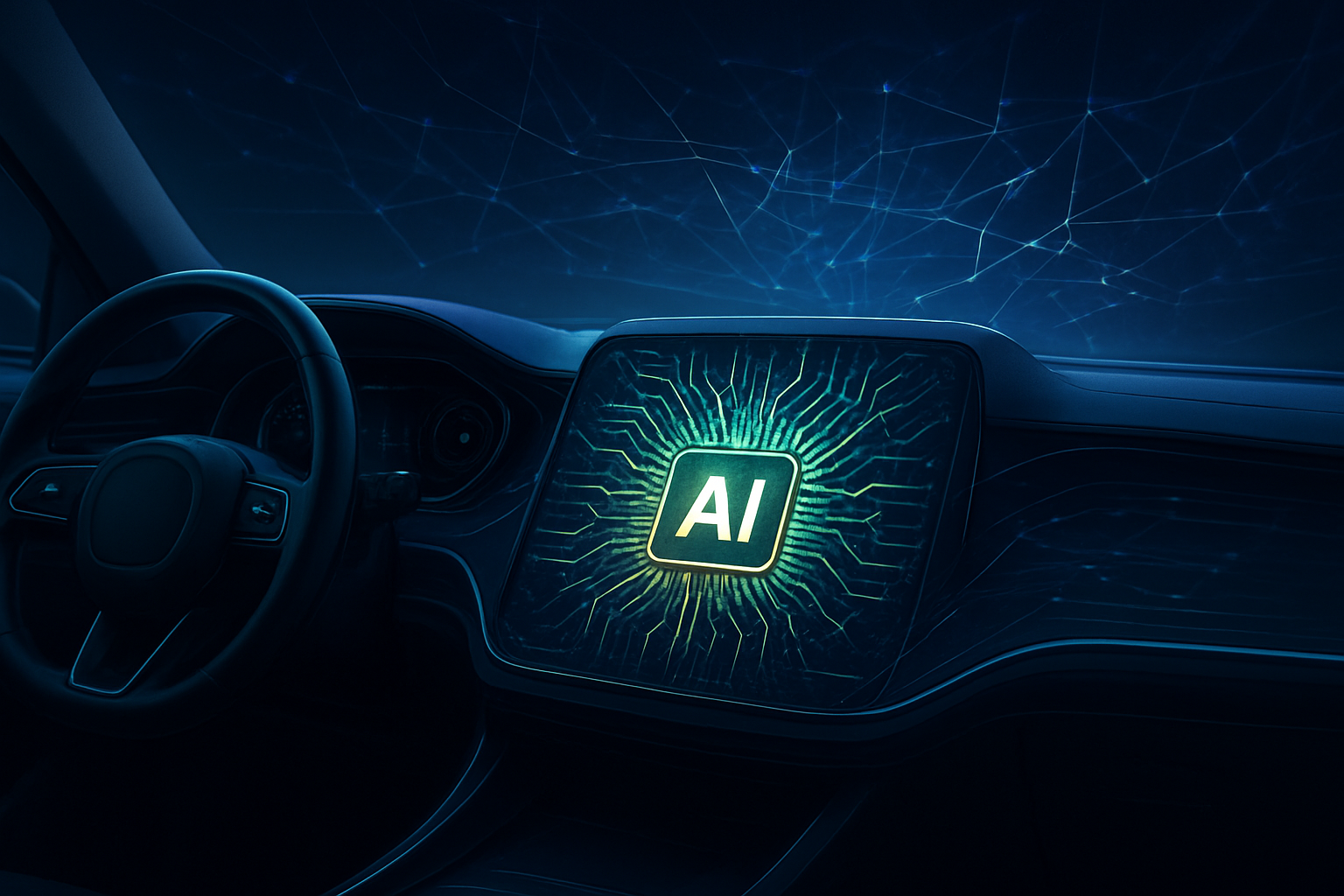
- Driving Edge AI and On-Device Processing: Late 2025 sees a significant shift towards "edge AI," where AI processing occurs locally on devices rather than solely in the cloud. Specialized accelerators are indispensable for enabling sophisticated AI on power-constrained devices like smartphones, IoT sensors, autonomous vehicles, and industrial robots. This trend reduces reliance on cloud computing, improves latency for real-time applications, and enhances data privacy. The edge AI accelerator market is projected to grow significantly, reaching approximately $10.13 billion in 2025 and an estimated $113.71 billion by 2034.
- Shaping Cloud AI Infrastructure: AI has become a foundational aspect of cloud architectures, with major cloud providers offering powerful AI accelerators like Google's (NASDAQ: GOOGL) TPUs and various GPUs to handle demanding machine learning tasks. A new class of "neoscalers" is emerging, focused on providing optimized GPU-as-a-Service (GPUaaS) for AI workloads, expanding accessibility and offering competitive pricing and flexible capacity.
- Prioritizing Sustainability and Energy Efficiency: The immense energy consumption of AI, particularly LLMs, has become a critical concern. Training and running these models require thousands of GPUs operating continuously, leading to high electricity usage, substantial carbon emissions, and significant water consumption for cooling data centers. This has made energy efficiency a top corporate priority by late 2025. Hardware innovations, including specialized accelerators, neuromorphic chips, optical processors, and advancements in FPGA architecture, are crucial for mitigating AI's environmental impact by offering significant energy savings and reducing the carbon footprint.
- Intensifying Competition and Innovation in the Hardware Market: The AI chip market is experiencing an "arms race," with intense competition among leading suppliers like NVIDIA (NASDAQ: NVDA), AMD (NASDAQ: AMD), and Intel (NASDAQ: INTC), as well as major hyperscalers (Amazon (NASDAQ: AMZN), Google, Microsoft (NASDAQ: MSFT), Meta (NASDAQ: META)) who are developing custom AI silicon. While NVIDIA maintains a strong lead in AI GPUs for training, competitors are gaining traction with cost-effective and energy-efficient alternatives, especially for inference workloads. The industry has moved to an annual product release cadence for AI accelerators, signifying rapid innovation.
Impacts:
- Unprecedented Performance and Efficiency: AI accelerators are delivering staggering performance improvements. Projections indicate a 300% performance improvement over traditional GPUs by 2025 for AI accelerators, with some specialized chips reportedly being 57 times faster in specific tasks. This superior speed, energy optimization, and cost-effectiveness are crucial for handling the escalating computational demands of modern AI.
- Enabling New AI Capabilities and Applications: This hardware revolution is enabling not just faster AI, but entirely new forms of AI that were previously computationally infeasible. It's pushing AI capabilities into areas like advanced natural language processing, complex computer vision, accelerated drug discovery, and highly autonomous systems.
- Significant Economic Impact: AI hardware has re-emerged as a strategic differentiator across industries, with the global AI chip market expected to surpass $150 billion in 2025. The intense competition and diversification of hardware solutions are anticipated to drive down costs, potentially democratizing access to powerful generative AI capabilities.
- Democratization of AI: Specialized accelerators, especially when offered through cloud services, lower the barrier to entry for businesses and researchers to leverage advanced AI. Coupled with the rise of open-source AI models and cloud-based AI services, this trend is making AI technologies more accessible to a wider audience beyond just tech giants.
Potential Concerns:
- Cost and Accessibility: Despite efforts toward democratization, the high cost and complexity associated with designing and manufacturing cutting-edge AI chips remain a significant barrier, particularly for startups. The transition to new accelerator architectures can also involve substantial investment.
- Vendor Lock-in and Standardization: The dominance of certain vendors (e.g., NVIDIA's strong market share in AI GPUs and its CUDA software ecosystem) raises concerns about potential vendor lock-in. The diverse and rapidly evolving hardware landscape also presents challenges in terms of compatibility and development learning curves.
- Environmental Impact: The "AI supercycle" is fueling unprecedented energy demand. Data centers, largely driven by AI, could account for a significant portion of global electricity usage (up to 20% by 2030-2035), leading to increased carbon emissions, excessive water consumption for cooling, and a growing problem of electronic waste from components like GPUs. The extraction of rare earth minerals for manufacturing these components also contributes to environmental degradation.
- Security Vulnerabilities: As AI workloads become more concentrated on specialized hardware, this infrastructure presents new attack surfaces that require robust security measures for data centers.
- Ethical Considerations: The push for more powerful hardware also implicitly carries ethical implications. Ensuring the trustworthiness, explainability, and fairness of AI systems becomes even more critical as their capabilities expand. Concerns about the lack of reliable and reproducible numerical foundations in current AI systems, which can lead to inconsistencies and "hallucinations," are driving research into "reasoning-native computing" to address precision and audibility.
Comparisons to Previous AI Milestones and Breakthroughs:
The current revolution in AI accelerators and specialized hardware is widely considered as transformative as the advent of GPUs for deep learning. Historically, advancements in AI have been intrinsically linked to the evolution of computing hardware.
- Early AI (1950s-1960s): Pioneers in AI faced severe limitations with room-sized mainframes that had minimal memory and slow processing speeds. Early programs, like Alan Turing's chess program, were too complex for the hardware of the time.
- The Rise of GPUs (2000s-2010s): The general-purpose parallel processing capabilities of GPUs, initially designed for graphics, proved incredibly effective for deep learning. This enabled researchers to train complex neural networks that were previously impractical, catalyzing the modern deep learning revolution. This represented a significant leap, allowing for a 50-fold increase in deep learning performance within three years by one estimate.
- The Specialized Hardware Era (2010s-Present): The current phase goes beyond general-purpose GPUs to purpose-built ASICs like Google's Tensor Processing Units (TPUs) and custom silicon from other tech giants. This shift from general-purpose computational brute force to highly refined, purpose-driven silicon marks a new era, enabling entirely new forms of AI that require immense computational resources rather than just making existing AI faster. For example, Google's sixth-generation TPUs (Trillium) offered a 4.7x improvement in compute performance per chip, necessary to keep pace with cutting-edge models involving trillions of calculations.
In late 2025, specialized AI hardware is not merely an evolutionary improvement but a fundamental re-architecture of how AI is computed, promising to accelerate innovation and embed intelligence more deeply into every facet of technology and society.
Future Developments
The landscape of AI accelerators and specialized hardware is undergoing rapid transformation, driven by the escalating computational demands of advanced artificial intelligence models. As of late 2025, experts anticipate significant near-term and long-term developments, ushering in new applications, while also highlighting crucial challenges that require innovative solutions.
Near-Term Developments (Late 2025 – 2027):
In the immediate future, the AI hardware sector will see several key advancements. The widespread adoption of 2nm chips in flagship consumer electronics and enterprise AI accelerators is expected, alongside the full commercialization of High-Bandwidth Memory (HBM4), which will dramatically increase memory bandwidth for AI workloads. Samsung (KRX: 005930) has already introduced 3nm Gate-All-Around (GAA) technology, with TSMC (NYSE: TSM) poised for mass production of 2nm chips in late 2025, and Intel (NASDAQ: INTC) aggressively pursuing its 1.8nm equivalent with RibbonFET GAA architecture. Advancements will also include Backside Power Delivery Networks (BSPDN) to optimize power efficiency. 2025 is predicted to be the year that AI inference workloads surpass training as the dominant AI workload, driven by the growing demand for real-time AI applications and autonomous "agentic AI" systems. This shift will fuel the development of more power-efficient alternatives to traditional GPUs, specifically tailored for inference tasks, challenging NVIDIA's (NASDAQ: NVDA) long-standing dominance. There is a strong movement towards custom AI silicon, including Application-Specific Integrated Circuits (ASICs), Neural Processing Units (NPUs), and Tensor Processing Units (TPUs), designed to handle specific tasks with greater speed, lower latency, and reduced energy consumption. While NVIDIA's Blackwell and the upcoming Rubin models are expected to fuel significant sales, the company will face intensifying competition, particularly from Qualcomm (NASDAQ: QCOM) and AMD (NASDAQ: AMD).
Long-Term Developments (Beyond 2027):
Looking further ahead, the evolution of AI hardware promises even more radical changes. The proliferation of heterogeneous integration and chiplet architectures will see specialized processing units and memory seamlessly integrated within a single package, optimizing for specific AI workloads, with 3D chip stacking projected to reach a market value of approximately $15 billion in 2025. Neuromorphic computing, inspired by the human brain, promises significant energy efficiency and adaptability for specialized edge AI applications. Intel (NASDAQ: INTC), with its Loihi series and the large-scale Hala Point system, is a key player in this area. While still in early stages, quantum computing integration holds immense potential, with first-generation commercial quantum computers expected to be used in tandem with classical AI approaches within the next five years. The industry is also exploring novel materials and architectures, including 2D materials, to overcome traditional silicon limitations, and by 2030, custom silicon is predicted to dominate over 50% of semiconductor revenue, with AI chipmakers diversifying into specialized verticals such as quantum-AI hybrid accelerators. Optical AI accelerator chips for 6G edge devices are also emerging, with commercial 6G services expected around 2030.
Potential Applications and Use Cases on the Horizon:
These hardware advancements will unlock a plethora of new AI capabilities and applications across various sectors. Edge AI processors will enable real-time, on-device AI processing in smartphones (e.g., real-time language translation, predictive text, advanced photo editing with Google's (NASDAQ: GOOGL) Gemini Nano), wearables, autonomous vehicles, drones, and a wide array of IoT sensors. Generative AI and LLMs will continue to be optimized for memory-intensive inference tasks. In healthcare, AI will enable precision medicine and accelerated drug discovery. In manufacturing and robotics, AI-powered robots will automate tasks and enhance smart manufacturing. Finance and business operations will see autonomous finance and AI tools boosting workplace productivity. Scientific discovery will benefit from accelerated complex simulations. Hardware-enforced privacy and security will become crucial for building user trust, and advanced user interfaces like Brain-Computer Interfaces (BCIs) are expected to expand human potential.
Challenges That Need to Be Addressed:
Despite these exciting prospects, several significant challenges must be tackled. The explosive growth of AI applications is putting immense pressure on data centers, leading to surging power consumption and environmental concerns. Innovations in energy-efficient hardware, advanced cooling systems, and low-power AI processors are critical. Memory bottlenecks and data transfer issues require parallel processing units and advanced memory technologies like HBM3 and CXL (Compute Express Link). The high cost of developing and deploying cutting-edge AI accelerators can create a barrier to entry for smaller companies, potentially centralizing advanced AI development. Supply chain vulnerabilities and manufacturing bottlenecks remain a concern. Ensuring software compatibility and ease of development for new hardware architectures is crucial for widespread adoption, as is confronting regulatory clarity, responsible AI principles, and comprehensive data management strategies.
Expert Predictions (As of Late 2025):
Experts predict a dynamic future for AI hardware. The global AI chip market is projected to surpass $150 billion in 2025 and is anticipated to reach $460.9 billion by 2034. The long-standing GPU dominance, especially in inference workloads, will face disruption as specialized AI accelerators offer more power-efficient alternatives. The rise of agentic AI and hybrid workforces will create conditions for companies to "employ" and train AI workers to be part of hybrid teams with humans. Open-weight AI models will become the standard, fostering innovation, while "expert AI systems" with advanced capabilities and industry-specific knowledge will emerge. Hardware will increasingly be designed from the ground up for AI, leading to a focus on open-source hardware architectures, and governments are investing hundreds of billions into domestic AI capabilities and sovereign AI cloud infrastructure.
In conclusion, the future of AI accelerators and specialized hardware is characterized by relentless innovation, driven by the need for greater efficiency, lower power consumption, and tailored solutions for diverse AI workloads. While traditional GPUs will continue to evolve, the rise of custom silicon, neuromorphic computing, and eventually quantum-AI hybrids will redefine the computational landscape, enabling increasingly sophisticated and pervasive AI applications across every industry. Addressing the intertwined challenges of energy consumption, cost, and supply chain resilience will be crucial for realizing this transformative potential.
Comprehensive Wrap-up
The landscape of Artificial Intelligence (AI) is being profoundly reshaped by advancements in AI accelerators and specialized hardware. As of late 2025, these critical technological developments are not only enhancing the capabilities of AI but also driving significant economic growth and fostering innovation across various sectors.
Summary of Key Takeaways:
AI accelerators are specialized hardware components, including Graphics Processing Units (GPUs), Tensor Processing Units (TPUs), Field-Programmable Gate Arrays (FPGAs), and Application-Specific Integrated Circuits (ASICs), designed to optimize and speed up AI workloads. Unlike general-purpose processors, these accelerators efficiently handle the complex mathematical computations—such as matrix multiplications—that are fundamental to AI tasks, particularly deep learning model training and inference. This specialization leads to faster performance, lower power consumption, and reduced latency, making real-time AI applications feasible. The market for AI accelerators is experiencing an "AI Supercycle," with sales of generative AI chips alone forecasted to surpass $150 billion in 2025. This growth is driven by an insatiable demand for computational power, fueling unprecedented hardware investment across the industry. Key trends include the transition from general-purpose CPUs to specialized hardware for AI, the critical role of these accelerators in scaling AI models, and their increasing deployment in both data centers and at the edge.
Significance in AI History:
The development of specialized AI hardware marks a pivotal moment in AI history, comparable to other transformative supertools like the steam engine and the internet. The widespread adoption of AI, particularly deep learning and large language models (LLMs), would be impractical, if not impossible, without these accelerators. The "AI boom" of the 2020s has been directly fueled by the ability to train and run increasingly complex neural networks efficiently on modern hardware. This acceleration has enabled breakthroughs in diverse applications such as autonomous vehicles, healthcare diagnostics, natural language processing, computer vision, and robotics. Hardware innovation continues to enhance AI performance, allowing for faster, larger, and more versatile models, which in turn enables real-time applications and scalability for enterprises. This fundamental infrastructure is crucial for processing and analyzing data, training models, and performing inference tasks at the immense scale required by today's AI systems.
Final Thoughts on Long-Term Impact:
The long-term impact of AI accelerators and specialized hardware will be transformative, fundamentally reshaping industries and societies worldwide. We can expect a continued evolution towards even more specialized AI chips tailored for specific workloads, such as edge AI inference or particular generative AI models, moving beyond general-purpose GPUs. The integration of AI capabilities directly into CPUs and Systems-on-Chips (SoCs) for client devices will accelerate, enabling more powerful on-device AI experiences.
One significant aspect will be the ongoing focus on energy efficiency and sustainability. AI model training is resource-intensive, consuming vast amounts of electricity and water, and contributing to electronic waste. Therefore, advancements in hardware, including neuromorphic chips and optical processors, are crucial for developing more sustainable AI. Neuromorphic computing, which mimics the brain's processing and storage mechanisms, is poised for significant growth, projected to reach $1.81 billion in 2025 and $4.1 billion by 2029. Optical AI accelerators are also emerging, leveraging light for faster and more energy-efficient data processing, with the market expected to grow from $1.03 billion in 2024 to $1.29 billion in 2025.
Another critical long-term impact is the democratization of AI, particularly through edge AI and AI PCs. Edge AI devices, equipped with specialized accelerators, will increasingly handle everyday inferences locally, reducing latency and reliance on cloud infrastructure. AI-enabled PCs are projected to account for 31% of the market by the end of 2025 and become the most commonly used PCs by 2029, bringing small AI models directly to users for enhanced productivity and new capabilities.
The competitive landscape will remain intense, with major players and numerous startups pushing the boundaries of what AI hardware can achieve. Furthermore, geopolitical considerations are shaping supply chains, with a trend towards "friend-shoring" or "ally-shoring" to secure critical raw materials and reduce technological gaps.
What to Watch for in the Coming Weeks and Months (Late 2025):
As of late 2025, several key developments and trends are worth monitoring:
- New Chip Launches and Architectures: Keep an eye on announcements from major players. NVIDIA's (NASDAQ: NVDA) Blackwell Ultra chip family is expected to be widely available in the second half of 2025, with the next-generation Vera Rubin GPU system slated for the second half of 2026. AMD's (NASDAQ: AMD) Instinct MI355X chip was released in June 2025, with the MI400 series anticipated in 2026, directly challenging NVIDIA's offerings. Qualcomm (NASDAQ: QCOM) is entering the data center AI accelerator market with its AI200 line shipping in 2026, followed by the AI250 in 2027, leveraging its mobile-rooted power efficiency. Google (NASDAQ: GOOGL) is advancing its Trillium TPU v6e and the upcoming Ironwood TPU v7, aiming for dramatic performance boosts in massive clusters. Intel (NASDAQ: INTC) continues to evolve its Core Ultra AI Series 2 processors (released late 2024) for the AI PC market, and its Jaguar Shores chip is expected in 2026.
- The Rise of AI PCs and Edge AI: Expect increasing market penetration of AI PCs, which are becoming a necessary investment for businesses. Developments in edge AI hardware will focus on minimizing data movement and implementing efficient arrays for ML inferencing, critical for devices like smartphones, wearables, and autonomous vehicles. NVIDIA's investment in Nokia (NYSE: NOK) to support enterprise edge AI and 6G in radio networks signals a growing trend towards processing AI closer to network nodes.
- Advances in Alternative Computing Paradigms: Continue to track progress in neuromorphic computing, with ongoing innovation in hardware and investigative initiatives pushing for brain-like, energy-efficient processing. Research into novel materials, such as mushroom-based memristors, hints at a future with more sustainable and energy-efficient bio-hardware for niche applications like edge devices and environmental sensors. Optical AI accelerators will also see advancements in photonic computing and high-speed optical interconnects.
- Software-Hardware Co-design and Optimization: The emphasis on co-developing hardware and software will intensify to maximize AI capabilities and avoid performance bottlenecks. Expect new tools and frameworks that allow for seamless integration and optimization across diverse hardware architectures.
- Competitive Dynamics and Supply Chain Resilience: The intense competition among established semiconductor giants and innovative startups will continue to drive rapid product advancements. Watch for strategic partnerships and investments that aim to secure supply chains and foster regional technology ecosystems, such as the Hainan-Southeast Asia AI Hardware Battle.
The current period is characterized by exponential growth and continuous innovation in AI hardware, cementing its role as the indispensable backbone of the AI revolution. The investments made and technologies developed in late 2025 will define the trajectory of AI for years to come.
This content is intended for informational purposes only and represents analysis of current AI developments.
TokenRing AI delivers enterprise-grade solutions for multi-agent AI workflow orchestration, AI-powered development tools, and seamless remote collaboration platforms.
For more information, visit https://www.tokenring.ai/.