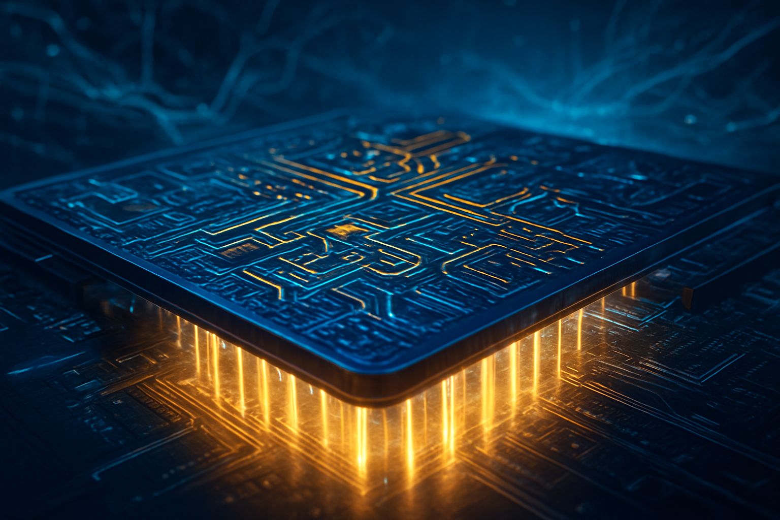
As of late January 2026, the semiconductor industry has reached a pivotal inflection point in the race for artificial intelligence supremacy. The transition to Backside Power Delivery Network (BS-PDN) technology—once a theoretical dream—has become the defining battlefield for chipmakers. With the recent high-volume rollout of Intel Corporation (NASDAQ: INTC) 18A process and the impending arrival of Taiwan Semiconductor Manufacturing Company (NYSE: TSM) A16 node, the "front-side" of the silicon wafer, long the congested highway for both data and electricity, is finally being decluttered to make way for the massive data throughput required by trillion-parameter AI models.
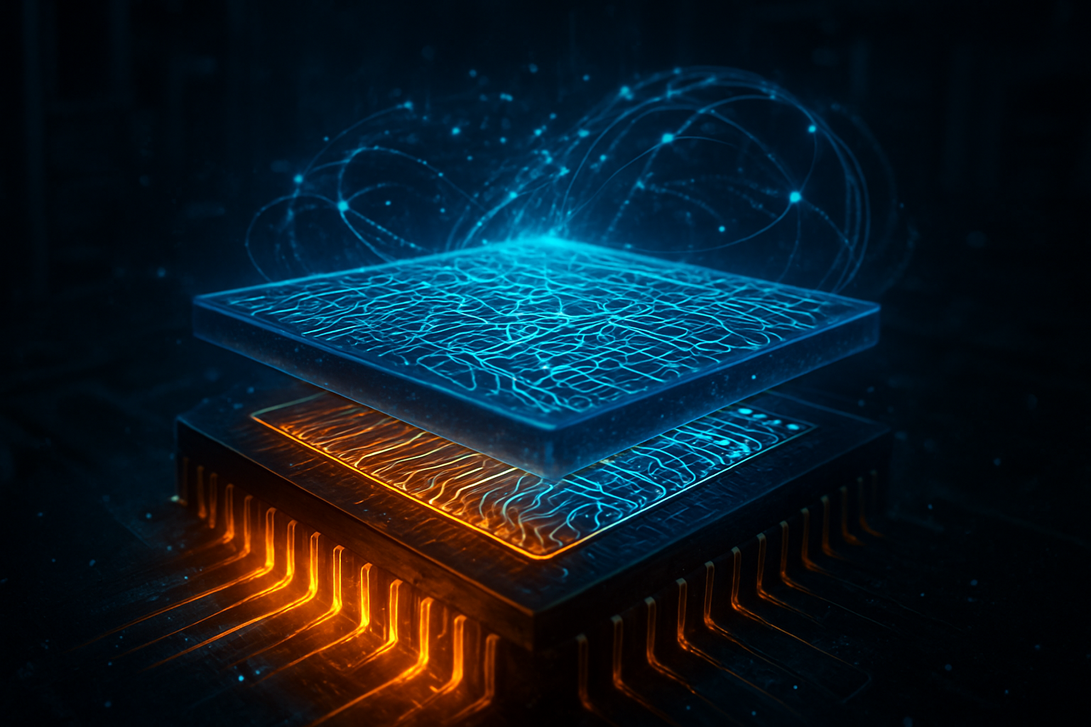
This architectural shift is more than a mere incremental update; it is a fundamental reimagining of chip design. By moving the power delivery wires to the literal "back" of the silicon wafer, manufacturers are solving the "voltage droop" (IR drop) problem that has plagued the industry as transistors shrunk toward the 1nm scale. For the first time, power and signal have their own dedicated real estate, allowing for a 10% frequency boost and a substantial reduction in power loss—gains that are critical as the energy consumption of data centers remains the primary bottleneck for AI expansion in 2026.
The Technical Duel: Intel’s PowerVia vs. TSMC’s Super Power Rail
The technical challenge behind BS-PDN involves flipping the traditional manufacturing process on its head. Historically, transistors were built first, followed by layers of metal interconnects for both power and signals. As these layers became increasingly dense, they acted like a bottleneck, causing electrical resistance that lowered the voltage reaching the transistors. Intel’s PowerVia, which debuted on the Intel 20A node and is now being mass-produced on 18A, utilizes Nano-Through Silicon Vias (nTSVs) to shuttle power from the backside directly to the transistor layer. These nTSVs are roughly 500 times smaller than traditional TSVs, minimizing the footprint and allowing for a reported 30% reduction in voltage droop.
In contrast, TSMC is preparing its A16 node (1.6nm), which features the "Super Power Rail." While Intel uses vias to bridge the gap, TSMC’s approach involves connecting the power network directly to the transistor’s source and drain. This "direct contact" method is technically more complex to manufacture but promises a 15% to 20% power reduction at the same speed compared to their 2nm (N2) offerings. By eliminating the need for power to weave through the "front-end-of-line" metal stacks, both companies have effectively decoupled the power and signal paths, reducing crosstalk and allowing for much wider, less resistive power wires on the back.
A New Arms Race for AI Giants and Foundry Customers
The implications for the competitive landscape of 2026 are profound. Intel’s first-mover advantage with PowerVia on the 18A node has allowed it to secure early foundry wins with major players like Microsoft Corporation (NASDAQ: MSFT) and Amazon.com, Inc. (NASDAQ: AMZN), who are eager to optimize their custom AI silicon. For Intel, 18A is a "make or break" moment to prove it can out-innovate TSMC in the foundry space. The 65% to 75% yields reported this month suggest that Intel is finally stabilizing its manufacturing, potentially reclaiming the process leadership it lost a decade ago.
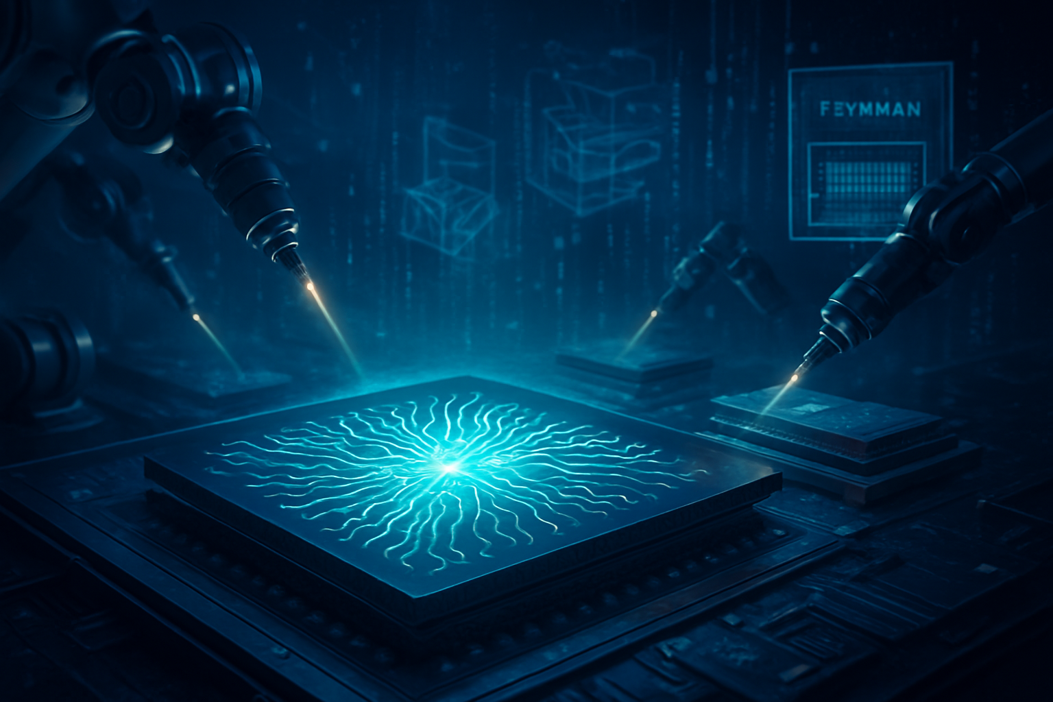
However, TSMC remains the preferred partner for NVIDIA Corporation (NASDAQ: NVDA). Earlier this month at CES 2026, NVIDIA teased its future "Feynman" GPU architecture, which is expected to be the "alpha" customer for TSMC’s A16 Super Power Rail. While NVIDIA's current "Rubin" platform relies on existing 2nm tech, the leap to A16 is predicted to deliver a 3x performance-per-watt improvement. This competition isn't just about speed; it's about the "Joule-per-Token" metric. As AI companies face mounting pressure over energy costs and environmental impact, the chipmaker that can deliver the most tokens for the least amount of electricity will win the lion's share of the enterprise market.
Beyond the Transistor: Scaling the Broader AI Landscape
BS-PDN is not just a solution for congestion; it is the enabler for the next generation of 1,000-watt "Superchips." As AI accelerators push toward and beyond the 1kW power envelope, traditional cooling and power delivery methods have reached their physical limits. The introduction of backside power allows for "double-sided cooling," where heat can be efficiently extracted from both the front and back of the silicon. This is a game-changer for the high-density liquid-cooled racks being deployed by specialized AI clouds.
When compared to previous milestones like the introduction of FinFET in 2011, BS-PDN is arguably more disruptive because it changes the entire physical flow of chip manufacturing. The industry is moving away from a 2D "printing" mindset toward a truly 3D integrated circuit (3DIC) paradigm. This transition does raise concerns, however; the complexity of thinning wafers and bonding them back-to-back increases the risk of mechanical failure and reduces initial yields. Yet, for the AI research community, these hardware breakthroughs are the only way to sustain the scaling laws that have fueled the explosion of generative AI.
The Horizon: 1nm and the Era of Liquid-Metal Delivery
Looking ahead to late 2026 and 2027, the focus will shift from simply implementing BS-PDN to optimizing it for 1nm nodes. Experts predict that the next evolution will involve integrating capacitors and voltage regulators directly onto the backside of the wafer, further reducing the distance power must travel. We are also seeing early research into liquid-metal power delivery systems that could theoretically allow for even higher current densities without the resistive heat of copper.
The main challenge remains the cost. High-NA EUV lithography from ASML Holding N.V. (NASDAQ: ASML) is required for these advanced nodes, and the machines currently cost upwards of $350 million each. Only a handful of companies can afford to design chips at this level. This suggests a future where the gap between "the haves" (those with access to BS-PDN silicon) and "the have-nots" continues to widen, potentially centralizing AI power even further among the largest tech conglomerates.
Closing the Loop on the Backside Revolution
The move to Backside Power Delivery marks the end of the "Planar Power" era. As Intel ramps up 18A and TSMC prepares the A16 Super Power Rail, the semiconductor industry has successfully bypassed one of its most daunting physical barriers. The key takeaways for 2026 are clear: power delivery is now as important as logic density, and the ability to manage thermal and electrical resistance at the atomic scale is the new currency of the AI age.
This development will go down in AI history as the moment hardware finally caught up with the ambitions of software. In the coming months, the industry will be watching the first benchmarks of Intel's Panther Lake and the final tape-outs of NVIDIA’s A16-based designs. If these chips deliver on their promises, the "Backside Revolution" will have provided the necessary oxygen for the AI fire to continue burning through the end of the decade.
This content is intended for informational purposes only and represents analysis of current AI developments.
TokenRing AI delivers enterprise-grade solutions for multi-agent AI workflow orchestration, AI-powered development tools, and seamless remote collaboration platforms.
For more information, visit https://www.tokenring.ai/.