As the global hunger for generative AI compute continues to outpace supply, the semiconductor landscape has reached a historic inflection point in early 2026. Intel (NASDAQ: INTC) has successfully leveraged its "Golden Ticket" opportunity, transforming from a legacy giant in recovery to a pivotal manufacturing partner for the world’s most advanced AI architects. In a move that has sent shockwaves through the industry, NVIDIA (NASDAQ: NVDA), the undisputed king of AI silicon, has reportedly begun shifting significant manufacturing and packaging orders to Intel Foundry, breaking its near-exclusive reliance on the Taiwan Semiconductor Manufacturing Company (NYSE: TSM).
The catalyst for this shift is a perfect storm of TSMC production bottlenecks and Intel’s technical resurgence. While TSMC’s advanced nodes remain the gold standard, the company has become a victim of its own success, with its Chip-on-Wafer-on-Substrate (CoWoS) packaging capacity sold out through the end of 2026. This supply-side choke point has left AI titans with a stark choice: wait in a multi-quarter queue for TSMC’s limited output or diversify their supply chains. Intel, having finally achieved high-volume manufacturing with its 18A process node, has stepped into the breach, positioning itself as the necessary alternative to stabilize the global AI economy.
Technical Superiority and the Power of 18A
The centerpiece of Intel’s comeback is the 18A (1.8nm-class) process node, which officially entered high-volume manufacturing at Intel’s Fab 52 facility in Arizona this month. Surpassing industry expectations, 18A yields are currently reported in the 65% to 75% range, a level of maturity that signals commercial viability for mission-critical AI hardware. Unlike previous nodes, 18A introduces two foundational innovations: RibbonFET (Gate-All-Around transistor architecture) and PowerVia (backside power delivery). PowerVia, in particular, has emerged as Intel's "secret sauce," reducing voltage droop by up to 30% and significantly improving performance-per-watt—a metric that is now more valuable than raw clock speed in the energy-constrained world of AI data centers.
Beyond the transistor level, Intel’s advanced packaging capabilities—specifically Foveros and EMIB (Embedded Multi-Die Interconnect Bridge)—have become its most immediate competitive advantage. While TSMC's CoWoS packaging has been the primary bottleneck for NVIDIA’s Blackwell and Rubin architectures, Intel has aggressively expanded its New Mexico packaging facilities, increasing Foveros capacity by 150%. This allows companies like NVIDIA to utilize Intel’s packaging "as a service," even for chips where the silicon wafers were produced elsewhere. Industry experts have noted that Intel’s EMIB-T technology allows for a relatively seamless transition from TSMC’s ecosystem, enabling chip designers to hit 2026 shipment targets that would have been impossible under a TSMC-only strategy.
The initial reactions from the AI research and hardware communities have been cautiously optimistic. While TSMC still maintains a slight edge in raw transistor density with its N2 node, the consensus is that Intel has closed the "process gap" for the first time in a decade. Technical analysts at several top-tier firms have pointed out that Intel’s lead in glass substrate development—slated for even broader adoption in late 2026—will offer superior thermal stability for the next generation of 3D-stacked superchips, potentially leapfrogging TSMC’s traditional organic material approach.
A Strategic Realignment for Tech Giants
The ramifications of Intel’s "Golden Ticket" extend far beyond its own balance sheet, altering the strategic positioning of every major player in the AI space. NVIDIA’s decision to utilize Intel Foundry for its non-flagship networking silicon and specialized H-series variants represents a masterful risk mitigation strategy. By diversifying its foundry partners, NVIDIA can bypass the "TSMC premium"—wafer prices that have climbed by double digits annually—while ensuring a steady flow of hardware to enterprise customers who are less dependent on the absolute cutting-edge performance of the upcoming Rubin R100 flagship.
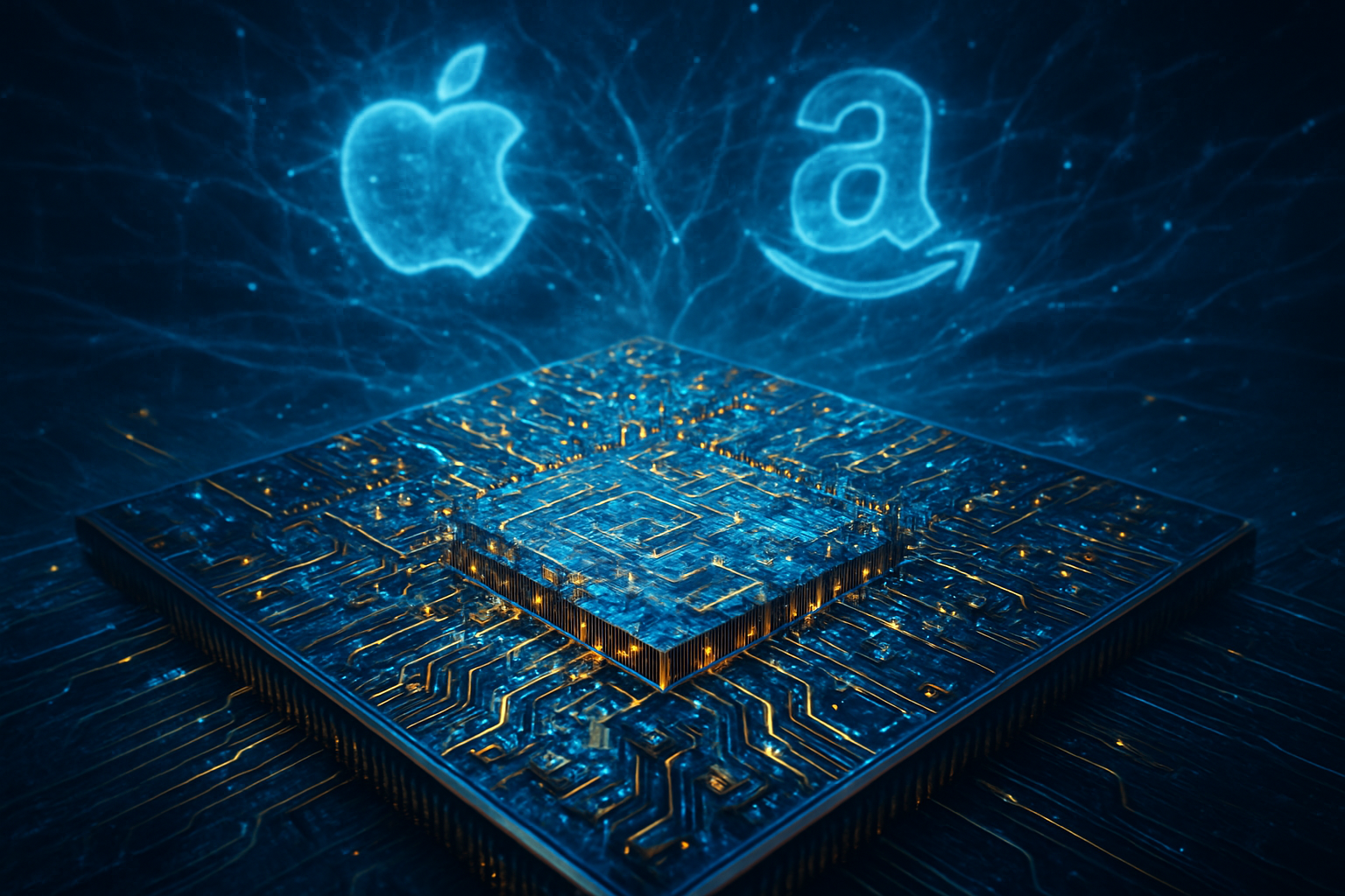
NVIDIA is not the only giant making the move; the "Foundry War" of 2026 has seen a flurry of new partnerships. Apple (NASDAQ: AAPL) has reportedly qualified Intel’s 18A node for a subset of its entry-level M-series chips, marking the first time the iPhone maker has moved away from TSMC exclusivity in nearly twenty years. Meanwhile, Microsoft (NASDAQ: MSFT) and Amazon (NASDAQ: AMZN) have solidified their roles as anchor customers, with Microsoft’s Maia AI accelerators and Amazon’s custom AI fabric chips now rolling off Intel’s Arizona production lines. This shift provides these companies with greater bargaining power against TSMC and insulates them from the geopolitical vulnerabilities associated with concentrated production in the Taiwan Strait.
For startups and specialized AI labs, Intel’s emergence provides a lifeline. During the "Compute Crunch" of 2024 and 2025, smaller players were often crowded out of TSMC’s production schedule by the massive orders from the "Magnificent Seven." Intel’s excess capacity and its eagerness to win market share have created a more democratic landscape, allowing second-tier AI chipmakers and custom ASIC vendors to bring their products to market faster. This disruption is expected to accelerate the development of "Sovereign AI" initiatives, where nations and regional clouds seek to build independent compute stacks on domestic soil.
The Geopolitical and Economic Landscape
Intel’s resurgence is inextricably linked to the broader trend of "Silicon Nationalism." In late 2025, the U.S. government effectively nationalized the success of Intel, with the administration taking a 9.9% equity stake in the company as part of a $8.9 billion investment. Combined with the $7.86 billion in direct funding from the CHIPS Act, Intel has gained access to nearly $57 billion in early cash, allowing it to accelerate the construction of massive "Silicon Heartland" hubs in Ohio and Arizona. This unprecedented level of state support has positioned Intel as the sole provider for the "Secure Enclave" program, a $3 billion initiative to ensure that the U.S. military and intelligence agencies have a trusted, domestic source of leading-edge AI silicon.
This shift marks a departure from the globalization-first era of the early 2000s. The "Golden Ticket" isn't just about manufacturing efficiency; it's about supply chain resilience. As the world moves toward 2027, the semiconductor industry is moving away from a single-choke-point model toward a multi-polar foundry system. While TSMC remains the most profitable entity in the ecosystem, it no longer holds the totalizing influence it once did. The transition mirrors previous industry milestones, such as the rise of fabless design in the 1990s, but with a modern twist: the physical location and political alignment of the fab now matter as much as the nanometer count.
However, this transition is not without concerns. Critics point out that the heavy government involvement in Intel could lead to market distortions or a "too big to fail" mentality that might stifle long-term innovation. Furthermore, while Intel has captured the "Golden Ticket" for now, the environmental impact of such a massive domestic manufacturing ramp-up—particularly regarding water usage in the American Southwest—remains a point of intense public and regulatory scrutiny.
The Horizon: 14A and the Road to 2027
Looking ahead, the next 18 to 24 months will be defined by the race toward the 1.4nm threshold. Intel is already teasing its 14A node, which is expected to enter risk production by early 2027. This next step will lean even more heavily on High-NA EUV (Extreme Ultraviolet) lithography, a technology where Intel has secured an early lead in equipment installation. If Intel can maintain its execution momentum, it could feasibly become the primary manufacturer for the next wave of "Edge AI" devices—smartphones and PCs that require massive on-device inference capabilities with minimal power draw.
The potential applications for this newfound capacity are vast. We are likely to see an explosion in highly specialized AI ASICs (Application-Specific Integrated Circuits) tailored for robotics, autonomous logistics, and real-time medical diagnostics. These chips require the advanced 3D-packaging that Intel has pioneered but at volumes that TSMC previously could not accommodate. Experts predict that by 2028, the "Intel-Inside" brand will be revitalized, not just as a processor in a laptop, but as the foundational infrastructure for the autonomous economy.
The immediate challenge for Intel remains scaling. Transitioning from successful "High-Volume Manufacturing" to "Global Dominance" requires a flawless logistical execution that the company has struggled with in the past. To maintain its "Golden Ticket," Intel must prove to customers like Broadcom (NASDAQ: AVGO) and AMD (NASDAQ: AMD) that it can sustain high yields consistently across multiple geographic sites, even as it navigates the complexities of integrated device manufacturing and third-party foundry services.
A New Era of Semiconductor Resilience
The events of early 2026 have rewritten the playbook for the AI industry. Intel’s ability to capitalize on TSMC’s bottlenecks has not only saved its own business but has provided a critical safety valve for the entire technology sector. The "Golden Ticket" opportunity has successfully turned the "chip famine" into a competitive market, fostering innovation and reducing the systemic risk of a single-source supply chain.
In the history of AI, this period will likely be remembered as the "Great Re-Invention" of the American foundry. Intel’s transformation into a viable, leading-edge alternative for companies like NVIDIA and Apple is a testament to the power of strategic technical pivots combined with aggressive industrial policy. As the first 18A-powered AI servers begin to ship to data centers this quarter, the industry's eyes will be fixed on the performance data.
In the coming weeks and months, watchers should look for the first formal performance benchmarks of NVIDIA-Intel hybrid products and any further shifts in Apple’s long-term silicon roadmap. While the "Foundry War" is far from over, for the first time in decades, the competition is truly global, and the stakes have never been higher.
This content is intended for informational purposes only and represents analysis of current AI developments.
TokenRing AI delivers enterprise-grade solutions for multi-agent AI workflow orchestration, AI-powered development tools, and seamless remote collaboration platforms. For more information, visit https://www.tokenring.ai/.