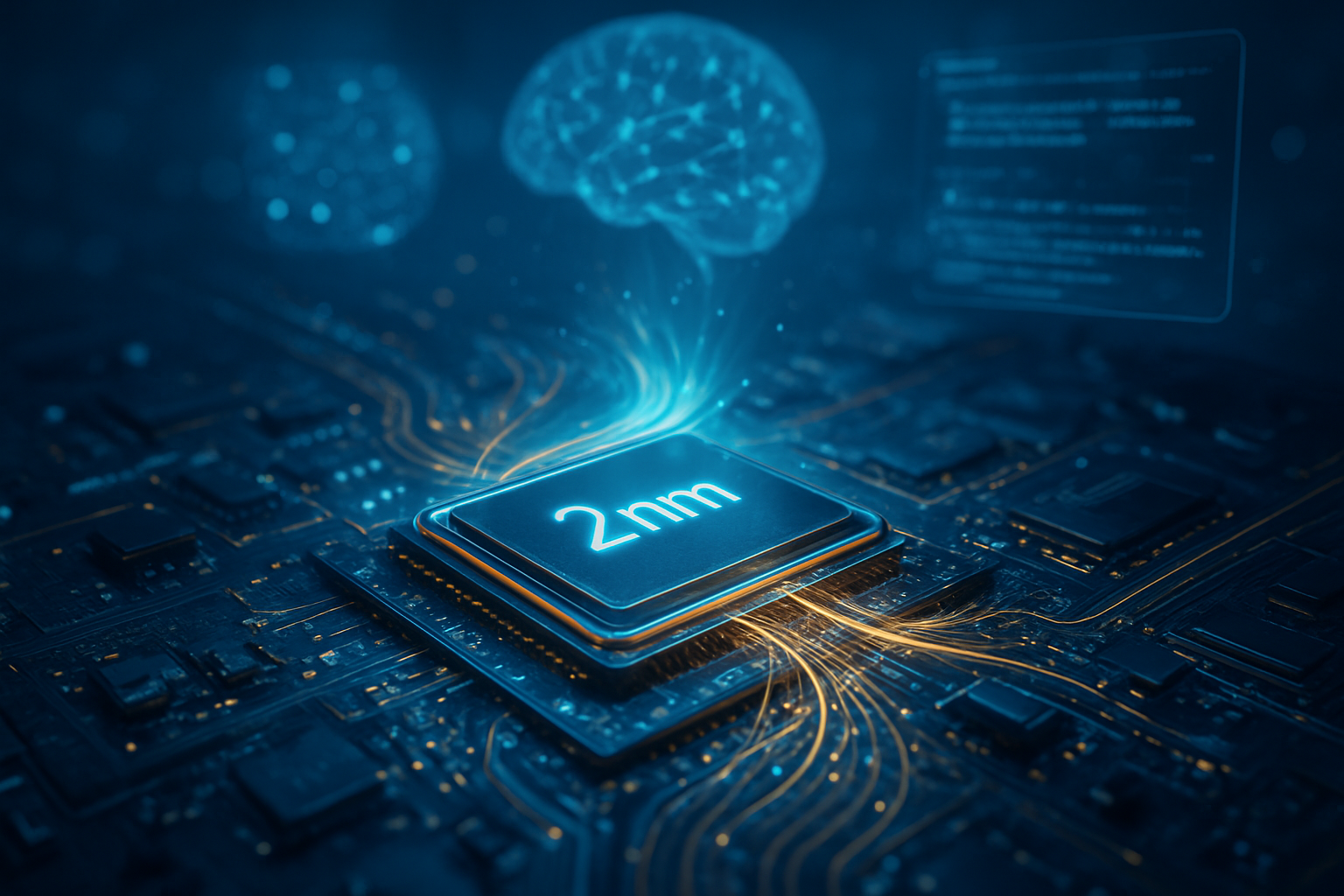
Tag: AI Chips

  • The GAA Era Arrives: TSMC Enters Mass Production of 2nm Chips to Fuel the Next AI Supercycle

    The GAA Era Arrives: TSMC Enters Mass Production of 2nm Chips to Fuel the Next AI Supercycle

    As the calendar turns to early 2026, the global semiconductor landscape has officially shifted on its axis. Taiwan Semiconductor Manufacturing Company (NYSE:TSM), commonly known as TSMC, has successfully crossed the finish line of its most ambitious technological transition in a decade. Following a rigorous ramp-up period that concluded in late 2025, the company’s 2nm (N2) node is now in high-volume manufacturing, ushering in the era of Gate-All-Around (GAA) nanosheet transistors. This milestone marks more than just a reduction in feature size; it represents the foundational infrastructure upon which the next generation of generative AI and high-performance computing (HPC) will be built.

    The immediate significance of this development cannot be overstated. By moving into volume production ahead of its most optimistic competitors and maintaining superior yield rates, TSMC has effectively secured its position as the primary engine of the AI economy. With primary production hubs at Fab 22 in Kaohsiung and Fab 20 in Hsinchu reaching a combined output of over 50,000 wafers per month this January, the company is already churning out the silicon that will power the most advanced smartphones and data center accelerators of 2026 and 2027.

    The Nanosheet Revolution: Engineering the Future of Silicon

    The N2 node represents a fundamental departure from the FinFET (Fin Field-Effect Transistor) architecture that has dominated the industry for the last several process generations. In traditional FinFETs, the gate controls the channel on three sides; however, as transistors shrink toward the 2nm threshold, current leakage becomes an insurmountable hurdle. TSMC’s shift to Gate-All-Around (GAA) nanosheet transistors solves this by wrapping the gate around all four sides of the channel, providing superior electrostatic control and drastically reducing power leakage.

    Technical specifications for the N2 node are staggering. Compared to the previous 3nm (N3E) process, the 2nm node offers a 10% to 15% increase in performance at the same power envelope, or a significant 25% to 30% reduction in power consumption at the same clock speed. Furthermore, the N2 node introduces "Super High-Performance Metal-Insulator-Metal" (SHPMIM) capacitors. These components double the capacitance density while cutting resistance by 50%, a critical advancement for AI chips that must handle massive, instantaneous power draws without losing efficiency. Early logic test chips have reportedly achieved yield rates between 70% and 80%, a metric that validates TSMC's manufacturing prowess compared to the more volatile early yields seen in rival GAA implementations.

    A High-Stakes Duel: Intel, Samsung, and the Battle for Foundry Supremacy

    The successful ramp of N2 has profound implications for the competitive balance between the "Big Three" chipmakers. While Samsung Electronics (KRX:005930) was technically the first to move to GAA at the 3nm stage, its yields have historically struggled to compete with the stability of TSMC. Samsung’s recent launch of the SF2 node and the Exynos 2600 chip shows progress, but the company remains primarily a secondary source for major designers. Meanwhile, Intel (NASDAQ:INTC) has emerged as a formidable challenger with its 18A node. Intel’s 18A utilizes "PowerVia" (Backside Power Delivery), a technology TSMC will not integrate until its N2P variant in late 2026. This gives Intel a temporary technical lead in raw power delivery metrics, even as TSMC maintains a superior transistor density of roughly 313 million transistors per square millimeter.

    For the world’s most valuable tech giants, the arrival of N2 is a strategic windfall. Apple (NASDAQ:AAPL), acting as TSMC’s "alpha" customer, has reportedly secured over 50% of the initial 2nm capacity to power its upcoming iPhone 18 series and the M5/M6 Mac silicon. Close on their heels is Nvidia (NASDAQ:NVDA), which is leveraging the N2 node for its next-generation AI platforms succeeding the Blackwell architecture. Other major players including Advanced Micro Devices (NASDAQ:AMD), Broadcom (NASDAQ:AVGO), and MediaTek (TPE:2454) have already finalized their 2026 production slots, signaling a collective industry bet that TSMC’s N2 will be the gold standard for efficiency and scale.

    Scaling AI: The Broader Landscape of 2nm Integration

    The transition to 2nm is inextricably linked to the trajectory of artificial intelligence. As Large Language Models (LLMs) grow in complexity, the demand for "compute" has become the defining constraint of the tech industry. The 25-30% power savings offered by N2 are not merely a luxury for mobile devices; they are a survival necessity for data centers. By reducing the energy required per inference or training cycle, 2nm chips allow hyperscalers like Microsoft (NASDAQ:MSFT) and Amazon (NASDAQ:AMZN) to pack more density into their existing power footprints, potentially slowing the skyrocketing environmental costs of the AI boom.

    This milestone also reinforces the "Moore's Law is not dead" narrative, albeit with a caveat: while transistor density continues to increase, the cost per transistor is rising. The complexity of GAA manufacturing requires multi-billion dollar investments in Extreme Ultraviolet (EUV) lithography and specialized cleanrooms. This creates a widening "innovation gap" where only the largest, most capitalized companies can afford the leap to 2nm, potentially consolidating power within a handful of AI leaders while leaving smaller startups to rely on older, less efficient silicon.

    The Roadmap Beyond: A16 and the 1.6nm Frontier

    The arrival of 2nm mass production is just the beginning of a rapid-fire roadmap. TSMC has already disclosed that its N2P node—the enhanced version of 2nm featuring Backside Power Delivery—is on track for mass production in late 2026. This will be followed closely by the A16 node (1.6nm) in 2027, which will incorporate "Super PowerRail" technology to further optimize power distribution directly to the transistor's source and drain.

    Experts predict that the next eighteen months will focus on "advanced packaging" as much as the nodes themselves. Technologies like CoWoS (Chip on Wafer on Substrate) will be essential to combine 2nm logic with high-bandwidth memory (HBM4) to create the massive AI "super-chips" of the future. The challenge moving forward will be heat dissipation; as transistors become more densely packed, managing the thermal output of these 2nm dies will require innovative liquid cooling and material science breakthroughs.

    Conclusion: A Pivot Point for the Digital Age

    TSMC’s successful transition to the 2nm N2 node in early 2026 stands as one of the most significant engineering feats of the decade. By navigating the transition from FinFET to GAA nanosheets while maintaining industry-leading yields, the company has solidified its role as the indispensable foundation of the AI era. While Intel and Samsung continue to provide meaningful competition, TSMC’s ability to scale this technology for giants like Apple and Nvidia ensures that the heartbeat of global innovation remains centered in Taiwan.

    In the coming months, the industry will watch closely as the first 2nm consumer devices hit the shelves and the first N2-based AI clusters go online. This development is more than a technical upgrade; it is the starting gun for a new epoch of computing performance, one that will determine the pace of AI advancement for years to come.


    This content is intended for informational purposes only and represents analysis of current AI developments.

    TokenRing AI delivers enterprise-grade solutions for multi-agent AI workflow orchestration, AI-powered development tools, and seamless remote collaboration platforms.
    For more information, visit https://www.tokenring.ai/.

  • Biren Technology’s Blockbuster IPO: A 119% Surge Signals China’s AI Chip Independence

    Biren Technology’s Blockbuster IPO: A 119% Surge Signals China’s AI Chip Independence

    The landscape of the global semiconductor industry shifted dramatically on January 2, 2026, as Shanghai Biren Technology (HKG: 6082) made its highly anticipated debut on the Hong Kong Stock Exchange. In a stunning display of investor confidence that defied ongoing geopolitical tensions, Biren’s shares skyrocketed by as much as 119% during intraday trading, eventually closing its first day up 76% from its offering price of HK$19.60. The IPO, which raised approximately HK$5.58 billion (US$717 million), was oversubscribed by retail investors a staggering 2,348 times, marking the most explosive tech debut in the region since the pre-2021 era.

    This landmark listing is more than just a financial success story; it represents a pivotal moment in China’s quest for silicon sovereignty. As US export controls continue to restrict access to high-end hardware from NVIDIA (NASDAQ: NVDA), Biren’s BR100 chip has emerged as the definitive domestic alternative. The massive capital infusion from the IPO is expected to accelerate Biren’s production scaling and R&D, providing a homegrown foundation for the next generation of Chinese large language models (LLMs) and autonomous systems.

    The BR100: Engineering Around the Sanction Wall

    The technical centerpiece of Biren’s market dominance is the BR100 series, a high-performance general-purpose GPU (GPGPU) designed specifically for large-scale AI training and inference. Built on the proprietary "BiLiren" architecture, the BR100 utilizes an advanced 7nm process and a sophisticated "chiplet" (multi-chip module) design. This approach allows Biren to bypass the reticle limits of traditional monolithic chips, packing 77 billion transistors into a single package. The BR100 delivers peak performance of 1024 TFLOPS in BF16 precision and features 64GB of HBM2E memory with 2.3 TB/s bandwidth.

    While NVIDIA’s newer Blackwell and Hopper architectures still hold a raw performance edge in global markets, the BR100 has become the "workhorse" of Chinese data centers. Industry experts note that Biren’s software stack, BIRENSU, has achieved high compatibility with mainstream AI frameworks like PyTorch and TensorFlow, significantly lowering the migration barrier for developers who previously relied on NVIDIA’s CUDA. This technical parity in real-world workloads has led many Chinese research institutions to conclude that the BR100 is no longer just a "stopgap" solution, but a competitive platform capable of sustaining China’s AI ambitions indefinitely.

    A Market Reshaped by "Buy Local" Mandates

    The success of Biren’s IPO is fundamentally reshaping the competitive dynamics between Western chipmakers and domestic Chinese firms. For years, NVIDIA (NASDAQ: NVDA) enjoyed a near-monopoly in China’s AI sector, but that dominance is eroding under the weight of trade restrictions and Beijing’s aggressive "buy local" mandates. Reports from early January 2026 suggest that the Chinese government has issued guidance to domestic tech giants to pause or reduce orders for NVIDIA’s H200 chips—which were briefly permitted under specific licenses—to protect and nurture newly listed domestic champions like Biren.

    This shift provides a strategic advantage to Biren and its domestic peers, such as the Baidu (NASDAQ: BIDU) spin-off Kunlunxin and Shanghai Iluvatar CoreX. These companies now enjoy a "captive market" where demand is guaranteed by policy rather than just performance. For major Chinese cloud providers and AI labs, the Biren IPO offers a degree of supply chain security that was previously unthinkable. By securing billions in capital, Biren can now afford to outbid competitors for limited domestic fabrication capacity at SMIC (HKG: 0981), further solidifying its position as the primary gatekeeper of China's AI infrastructure.

    The Vanguard of a New AI Listing Wave

    Biren’s explosive debut is the lead domino in what is becoming a historic wave of Chinese AI and semiconductor listings in Hong Kong. Following Biren’s lead, the first two weeks of January 2026 saw a flurry of activity: the "AI Tiger" MiniMax Group surged 109% on its debut, and the Tsinghua-linked Zhipu AI raised over US$550 million. This trend signals that international investors are still hungry for exposure to the Chinese AI market, provided those companies can demonstrate a clear path to bypassing US technological bottlenecks.

    This development serves as a stark comparison to previous AI milestones. While the 2010s were defined by software-driven growth and mobile internet dominance, the mid-2020s are being defined by the "Hardware Renaissance." The fact that Biren was added to the US Entity List in 2023—an action meant to stifle its growth—has ironically served as a catalyst for its public success. By forcing the company to pivot to domestic foundries and innovate in chiplet packaging, the sanctions inadvertently created a battle-hardened champion that is now too well-capitalized to be easily suppressed.

    Future Horizons: Scaling and the HBM Challenge

    Looking ahead, Biren’s primary challenge will be scaling production to meet the insatiable demand of China’s "War of a Thousand Models." While the IPO provides the necessary cash, the company remains vulnerable to potential future restrictions on High-Bandwidth Memory (HBM) and advanced lithography tools. Analysts predict that Biren will use a significant portion of its IPO proceeds to secure long-term HBM supply contracts and to co-develop next-generation 2.5D packaging solutions with SMIC (HKG: 0981) and other domestic partners.

    In the near term, the industry is watching for the announcement of the BR200, which is rumored to utilize even more aggressive chiplet configurations to bridge the gap with NVIDIA’s 2026 product roadmap. Furthermore, there is growing speculation that Biren may begin exporting its hardware to "Global South" markets that are wary of US tech hegemony, potentially creating a secondary global ecosystem for AI hardware that operates entirely outside of the Western sphere of influence.

    A New Chapter in the Global AI Race

    The blockbuster IPO of Shanghai Biren Technology marks a definitive end to the era of undisputed Western dominance in AI hardware. With a 119% surge and billions in new capital, Biren has proven that the combination of state-backed demand and private market enthusiasm can overcome even the most stringent export controls. As of January 13, 2026, the company stands as a testament to the resilience of China’s semiconductor ecosystem and a warning to global competitors that the "silicon curtain" has two sides.

    In the coming weeks, the market will be closely monitoring the performance of other upcoming AI listings, including the expected spin-off of Baidu’s (NASDAQ: BIDU) Kunlunxin. If these debuts mirror Biren’s success, 2026 will be remembered as the year the center of gravity for AI hardware investment began its decisive tilt toward the East. For now, Biren has set the gold standard, proving that in the high-stakes world of artificial intelligence, independence is the ultimate competitive advantage.


    This content is intended for informational purposes only and represents analysis of current AI developments.

    TokenRing AI delivers enterprise-grade solutions for multi-agent AI workflow orchestration, AI-powered development tools, and seamless remote collaboration platforms.
    For more information, visit https://www.tokenring.ai/.

  • Samsung’s 2nm GAA Gambit: The High-Stakes Race to Topple TSMC’s Silicon Throne

    Samsung’s 2nm GAA Gambit: The High-Stakes Race to Topple TSMC’s Silicon Throne

    As the calendar turns to January 12, 2026, the global semiconductor landscape is witnessing a seismic shift. Samsung Electronics (KRX: 005930) has officially entered the era of high-volume 2nm production, leveraging its multi-year head start in Gate-All-Around (GAA) transistor architecture to challenge the long-standing dominance of Taiwan Semiconductor Manufacturing Company (NYSE: TSM). With the launch of the Exynos 2600 and a landmark manufacturing deal with Tesla (NASDAQ: TSLA), Samsung is no longer just a fast follower; it is positioning itself as the primary architect of the next generation of AI-optimized silicon.

    The immediate significance of this development cannot be overstated. By successfully transitioning its SF2 (2nm) node into mass production by late 2025, Samsung has effectively closed the performance gap that plagued its 5nm and 4nm generations. For the first time in nearly a decade, the foundry market is seeing a legitimate two-horse race at the leading edge, providing much-needed supply chain relief and competitive pricing for AI giants and automotive innovators who have grown weary of TSMC’s premium "monopoly pricing."

    Technical Mastery: Third-Generation GAA and the SF2 Roadmap

    Samsung’s 2nm strategy is built on the foundation of its Multi-Bridge Channel FET (MBCFET), a proprietary version of GAA technology that it first introduced with its 3nm node in 2022. While TSMC (NYSE: TSM) is only now transitioning to its first generation of Nanosheet (GAA) transistors with the N2 node, Samsung is already deploying its third-generation GAA architecture. This maturity has allowed Samsung to achieve stabilized yield rates between 50% and 60% for its SF2 node—a significant milestone that has bolstered industry confidence.

    The technical specifications of the SF2 node represent a massive leap over previous FinFET-based technologies. Compared to the 3nm SF3 process, the 2nm SF2 node delivers a 25% increase in power efficiency, a 12% boost in performance, and a 5% reduction in die area. To meet diverse market demands, Samsung has bifurcated its roadmap into specialized variants: SF2P for high-performance mobile, SF2X for high-performance computing (HPC) and AI data centers, and SF2A for the rigorous safety standards of the automotive industry.

    Initial reactions from the semiconductor research community have been notably positive. Early benchmarks of the Exynos 2600, manufactured on the SF2 node, indicate a 39% improvement in CPU performance and a staggering 113% boost in generative AI tasks compared to its predecessor. This performance parity with industry leaders suggests that Samsung’s early bet on GAA is finally paying dividends, offering a technical alternative that matches or exceeds the thermal and power envelopes of contemporary Apple (NASDAQ: AAPL) and Qualcomm (NASDAQ: QCOM) chips.

    Shifting the Balance of Power: Market Implications and Customer Wins

    The competitive implications of Samsung’s 2nm success are reverberating through the halls of Silicon Valley. Perhaps the most significant blow to the status quo is Samsung’s reported $16.5 billion agreement with Tesla to manufacture the AI5 and AI6 chips for Full Self-Driving (FSD) and the Optimus robotics platform. This deal positions Samsung’s new Taylor, Texas facility as a critical hub for "Made in USA" advanced silicon, directly challenging Intel (NASDAQ: INTC) Foundry’s ambitions to become the primary domestic alternative to Asian manufacturing.

    Furthermore, the pricing delta between Samsung and TSMC has become a pivotal factor for fabless companies. With TSMC’s 2nm wafers reportedly priced at upwards of $30,000, Samsung’s aggressive $20,000-per-wafer strategy for SF2 is attracting significant interest. Qualcomm (NASDAQ: QCOM) has already confirmed that it is exchanging 2nm wafers with Samsung for performance modifications, signaling a potential return to a dual-sourcing strategy for its flagship Snapdragon processors—a move that could significantly reduce costs for smartphone manufacturers globally.

    For AI labs and startups, Samsung’s SF2X node offers a specialized pathway for custom AI accelerators. Japanese AI unicorn Preferred Networks (PFN) has already signed on as a lead customer for SF2X, seeking to leverage the node's optimized power delivery for its next-generation deep learning processors. This diversification of the client base suggests that Samsung is successfully shedding its image as a "captive foundry" primarily serving its own mobile division, and is instead becoming a true merchant foundry for the AI era.

    The Broader AI Landscape: Efficiency in the Age of LLMs

    Samsung’s 2nm breakthrough fits into a broader trend where energy efficiency is becoming the primary metric for AI hardware success. As Large Language Models (LLMs) grow in complexity, the power consumption of data centers has become a bottleneck for scaling. The GAA architecture’s superior control over "leakage" current makes it inherently more efficient than the aging FinFET design, making Samsung’s 2nm nodes particularly attractive for the sustainable scaling of AI infrastructure.

    This development also marks the definitive end of the FinFET era at the leading edge. By successfully navigating the transition to GAA ahead of its rivals, Samsung has proven that the technical hurdles of Nanosheet transistors—while immense—are surmountable at scale. This milestone mirrors previous industry shifts, such as the move to High-K Metal Gate (HKMG) or the adoption of EUV lithography, serving as a bellwether for the next decade of semiconductor physics.

    However, concerns remain regarding the long-term yield stability of Samsung’s more advanced variants. While 50-60% yield is a victory compared to previous years, it still trails TSMC’s reported 70-80% yields for N2. The industry is watching closely to see if Samsung can maintain these yields as it scales to the SF2Z node, which will introduce Backside Power Delivery Network (BSPDN) technology in 2027. This technical "holy grail" aims to move power rails to the back of the wafer to further reduce voltage drop, but it adds another layer of manufacturing complexity.

    Future Horizons: From 2nm to the 1.4nm Frontier

    Looking ahead, Samsung is not resting on its 2nm laurels. The company has already outlined a clear roadmap for the SF1.4 (1.4nm) node, targeted for mass production in 2027. This future node is expected to integrate even more sophisticated AI-specific hardware optimizations, such as in-memory computing features and advanced 3D packaging solutions like SAINT (Samsung Advanced Interconnect Technology).

    In the near term, the industry is anticipating the full activation of the Taylor, Texas fab in late 2026. This facility will be the ultimate test of Samsung’s ability to replicate its Korean manufacturing excellence on foreign soil. If successful, it will provide a blueprint for a more geographically resilient semiconductor supply chain, reducing the world’s over-reliance on a single geographic point of failure in the Taiwan Strait.

    Experts predict that the next two years will be defined by a "yield war." As NVIDIA (NASDAQ: NVDA) and other AI titans begin to design for 2nm, the foundry that can provide the highest volume of functional chips at the lowest cost will capture the lion's share of the generative AI boom. Samsung’s current momentum suggests it is well-positioned to capture a significant portion of this market, provided it can continue to refine its GAA process.

    Conclusion: A New Chapter in Semiconductor History

    Samsung’s 2nm GAA strategy represents a bold and successful gamble that has fundamentally altered the competitive dynamics of the semiconductor industry. By embracing GAA architecture years before its competitors, Samsung has overcome its past yield struggles to emerge as a formidable challenger to TSMC’s crown. The combination of the SF2 node’s technical performance, aggressive pricing, and strategic U.S.-based manufacturing makes Samsung a critical player in the global AI infrastructure race.

    This development will be remembered as the moment the foundry market returned to true competition. For the tech industry, this means faster innovation, more diverse hardware options, and a more robust supply chain. For Samsung, it is a validation of its long-term R&D investments and a clear signal that it intends to lead, rather than follow, in the silicon-driven future.

    In the coming months, the industry will be watching the real-world performance of the Galaxy S26 and the first "Made in USA" 2nm wafers from Texas. These milestones will determine if Samsung’s 2nm gambit is a temporary surge or the beginning of a new era of silicon supremacy.


    This content is intended for informational purposes only and represents analysis of current AI developments.

    TokenRing AI delivers enterprise-grade solutions for multi-agent AI workflow orchestration, AI-powered development tools, and seamless remote collaboration platforms.
    For more information, visit https://www.tokenring.ai/.

  • The Glass Age: Why Intel and Samsung are Betting on Glass to Power 1,000-Watt AI Chips

    The Glass Age: Why Intel and Samsung are Betting on Glass to Power 1,000-Watt AI Chips

    As of January 2026, the semiconductor industry has officially entered what historians may one day call the "Glass Age." For decades, the foundation of chip packaging relied on organic resins, but the relentless pursuit of artificial intelligence has pushed these materials to their physical breaking point. With the latest generation of AI accelerators now demanding upwards of 1,000 watts of power, industry titans like Intel and Samsung have pivoted to glass substrates—a revolutionary shift that promises to solve the thermal and structural crises currently bottlenecking the world’s most powerful hardware.

    The transition is more than a mere material swap; it is a fundamental architectural redesign of how chips are built. By replacing traditional organic substrates with glass, manufacturers are overcoming the "warpage wall" that has plagued large-scale multi-die packages. This development is essential for the rollout of next-generation AI platforms, such as NVIDIA’s recently announced Rubin architecture, which requires the unprecedented stability and interconnect density that only glass can provide to manage its massive compute and memory footprint.

    Engineering the Transparent Revolution: TGVs and the Warpage Wall

    The technical shift to glass is necessitated by the extreme heat and physical size of modern AI "super-chips." Traditional organic substrates, typically made of Ajinomoto Build-up Film (ABF), have a high Coefficient of Thermal Expansion (CTE) that differs significantly from the silicon chips they support. As a 1,000-watt AI chip heats up, the organic substrate expands at a different rate than the silicon, causing the package to bend—a phenomenon known as the "warpage wall." Glass, however, can have its CTE precisely tuned to match silicon, reducing structural warpage by an estimated 70%. This allows for the creation of massive, ultra-flat packages exceeding 100mm x 100mm, which were previously impossible to manufacture with high yields.

    Beyond structural integrity, glass offers superior electrical properties. Through-Glass Vias (TGVs) are laser-etched into the substrate rather than mechanically drilled, allowing for a tenfold increase in routing density. This enables pitches of less than 10μm, allowing for significantly more data lanes between the GPU and its memory. Furthermore, glass's dielectric properties reduce signal transmission loss at high frequencies (10GHz+) by over 50%. This improved signal integrity means that data movement within the package consumes roughly half the power of traditional methods, a critical efficiency gain for data centers struggling with skyrocketing electricity demands.

    The industry is also moving away from circular 300mm wafers toward large 600mm x 600mm rectangular glass panels. This "Rectangular Revolution" increases area utilization from 57% to over 80%. By processing more chips simultaneously on a larger surface area, manufacturers can significantly increase throughput, helping to alleviate the global shortage of high-end AI silicon. Initial reactions from the research community suggest that glass substrates are the single most important advancement in semiconductor packaging since the introduction of CoWoS (Chip-on-Wafer-on-Substrate) nearly a decade ago.

    The Competitive Landscape: Intel’s Lead and Samsung’s Triple Alliance

    Intel Corporation (NASDAQ: INTC) has secured a significant first-mover advantage in this space. Following a billion-dollar investment in its Chandler, Arizona, facility, Intel is now in high-volume manufacturing (HVM) for glass substrates. At CES 2026, the company showcased its 18A (2nm-class) process node integrated with glass cores, powering the new Xeon 6+ "Clearwater Forest" server processors. By successfully commercializing glass substrates ahead of its rivals, Intel has positioned its Foundry Services as the premier destination for AI chip designers who need to package the world's most complex multi-die systems.

    Samsung Electronics (KRX: 005930) has responded with its "Triple Alliance" strategy, integrating its Electronics, Display, and Electro-Mechanics (SEMCO) divisions to fast-track its own glass substrate roadmap. By leveraging its world-class expertise in display glass, Samsung has brought a high-volume pilot line in Sejong, South Korea, into full operation as of early 2026. Samsung is specifically targeting the integration of HBM4 (High Bandwidth Memory) with glass interposers, aiming to provide a thermal solution for the memory-intensive needs of NVIDIA (NASDAQ: NVDA) and Advanced Micro Devices (NASDAQ: AMD).

    This shift creates a new competitive frontier for major AI labs and tech giants. Companies like NVIDIA and AMD are no longer just competing on transistor density; they are competing on packaging sophistication. NVIDIA's Rubin architecture, which entered production in early 2026, relies heavily on glass to maintain the integrity of its massive HBM4 arrays. Meanwhile, AMD has reportedly secured a deal with Absolics, a subsidiary of SKC (KRX: 011790), to utilize their Georgia-based glass substrate facility for the Instinct MI400 series. For these companies, glass substrates are not just an upgrade—they are the only way to keep the performance gains of "Moore’s Law 2.0" alive.

    A Wider Significance: Overcoming the Memory Wall and Optical Integration

    The adoption of glass substrates represents a pivotal moment in the broader AI landscape, signaling a move toward more integrated and efficient computing architectures. For years, the "memory wall"—the bottleneck caused by the slow transfer of data between processors and memory—has limited AI performance. Glass substrates enable much tighter integration of memory stacks, effectively doubling the bandwidth available to Large Language Models (LLMs). This allows for the training of even larger models with trillions of parameters, which were previously constrained by the physical limits of organic packaging.

    Furthermore, the transparency and flatness of glass open the door to Co-Packaged Optics (CPO). Unlike opaque organic materials, glass allows for the direct integration of optical interconnects within the chip package. This means that instead of using copper wires to move data, which generates heat and loses signal over distance, chips can use light. Experts believe this will eventually lead to a 50-90% reduction in the energy required for data movement, addressing one of the most significant environmental concerns regarding the growth of AI data centers.

    This milestone is comparable to the industry's shift from aluminum to copper interconnects in the late 1990s. It is a fundamental change in the "DNA" of the computer chip. However, the transition is not without its challenges. The current cost of glass substrates remains three to five times higher than organic alternatives, and the fragility of glass during the manufacturing process requires entirely new handling equipment. Despite these hurdles, the performance necessity of 1,000-watt chips has made the "Glass Age" an inevitability rather than an option.

    The Horizon: HBM4 and the Path to 2030

    Looking ahead, the next two to three years will see glass substrates move from high-end AI accelerators into more mainstream high-performance computing (HPC) and eventually premium consumer electronics. By 2027, it is expected that HBM4 will be the standard memory paired with glass-based packages, providing the massive throughput required for real-time generative video and complex scientific simulations. As manufacturing processes mature and yields improve, analysts predict that the cost premium of glass will drop by 40-60% by the end of the decade, making it the standard for all data center silicon.

    The long-term potential for optical computing remains the most exciting frontier. With glass substrates as the foundation, we may see the first truly hybrid electronic-photonic processors by 2030. These chips would use electricity for logic and light for communication, potentially breaking the power-law constraints that have slowed the advancement of traditional silicon. The primary challenge remains the development of standardized "glass-ready" design tools for chip architects, a task currently being tackled by major EDA (Electronic Design Automation) firms.

    Conclusion: A New Foundation for Intelligence

    The shift to glass substrates marks the end of the organic era and the beginning of a more resilient, efficient, and dense future for semiconductor packaging. By solving the critical issues of thermal expansion and signal loss, Intel, Samsung, and their partners have cleared the path for the 1,000-watt chips that will power the next decade of AI breakthroughs. This development is a testament to the industry's ability to innovate its way out of physical constraints, ensuring that the hardware can keep pace with the exponential growth of AI software.

    As we move through 2026, the industry will be watching the ramp-up of Intel’s 18A production and Samsung’s HBM4 integration closely. The success of these programs will determine the pace at which the next generation of AI models can be deployed. While the "Glass Age" is still in its early stages, its significance in AI history is already clear: it is the foundation upon which the future of artificial intelligence will be built.


    This content is intended for informational purposes only and represents analysis of current AI developments.

    TokenRing AI delivers enterprise-grade solutions for multi-agent AI workflow orchestration, AI-powered development tools, and seamless remote collaboration platforms.
    For more information, visit https://www.tokenring.ai/.

  • The Nanosheet Revolution: TSMC Commences Volume Production of 2nm Chips to Power the AI Supercycle

    The Nanosheet Revolution: TSMC Commences Volume Production of 2nm Chips to Power the AI Supercycle

    As of January 12, 2026, the global semiconductor landscape has officially entered its most transformative era in over a decade. Taiwan Semiconductor Manufacturing Company (NYSE:TSM / TPE:2330), the world’s largest contract chipmaker, has confirmed that its 2-nanometer (N2) process node is now in high-volume manufacturing (HVM). This milestone marks the end of the "FinFET" transistor era and the beginning of the "Nanosheet" era, providing the essential hardware foundation for the next generation of generative AI models, autonomous systems, and ultra-efficient mobile devices.

    The shift to 2nm is more than a incremental upgrade; it is a fundamental architectural pivot designed to overcome the "power wall" that has threatened to stall AI progress. By delivering a staggering 30% reduction in power consumption compared to current 3nm technologies, TSMC is enabling a future where massive Large Language Models (LLMs) can run with significantly lower energy footprints. This announcement solidifies TSMC’s dominance in the foundry market, as the company scales production to meet the insatiable demand from the world's leading technology giants.

    The Technical Leap: From Fins to Nanosheets

    The core of the N2 node’s success lies in the transition from FinFET (Fin Field-Effect Transistor) to Gate-All-Around (GAA) Nanosheet transistors. For nearly 15 years, FinFET served the industry well, but as transistors shrunk toward the atomic scale, current leakage became an insurmountable hurdle. The Nanosheet design solves this by stacking horizontal layers of silicon and surrounding them on all four sides with the gate. This 360-degree control virtually eliminates leakage, allowing for tighter electrostatic management and drastically improved energy efficiency.

    Technically, the N2 node offers a "full-node" leap over the previous N3E (3nm) process. According to TSMC’s engineering data, the 2nm process delivers a 10% to 15% performance boost at the same power level, or a 25% to 30% reduction in power consumption at the same clock speed. Furthermore, TSMC has introduced a proprietary technology called Nano-Flex™. This allows chip designers to mix and match nanosheets of different heights within a single block—using "tall" nanosheets for high-performance compute cores and "short" nanosheets for energy-efficient background tasks. This level of granularity is unprecedented and gives designers a new toolkit for balancing the thermal and performance needs of complex AI silicon.

    Initial reports from the Hsinchu and Kaohsiung fabs indicate that yield rates for the N2 node are remarkably mature, sitting between 65% and 75%. This is a significant achievement for a first-generation architectural shift, as new nodes typically struggle to reach such stability in their first few months of volume production. The integration of "Super-High-Performance Metal-Insulator-Metal" (SHPMIM) capacitors further enhances the node, providing double the capacitance density and a 50% reduction in resistance, which ensures stable power delivery for the high-frequency bursts required by AI inference engines.

    The Industry Impact: Securing the AI Supply Chain

    The commencement of 2nm production has sparked a gold rush among tech titans. Apple (NASDAQ:AAPL) has reportedly secured over 50% of TSMC’s initial N2 capacity through 2026. The upcoming A20 Pro chip, expected to power the next generation of iPhones and iPads, will likely be the first consumer-facing product to utilize this technology, giving Apple a significant lead in on-device "Edge AI" capabilities. Meanwhile, NVIDIA (NASDAQ:NVDA) and AMD (NASDAQ:AMD) are racing to port their next-generation AI accelerators to the N2 node. NVIDIA’s rumored "Vera Rubin" architecture and AMD’s "Venice" EPYC processors are expected to leverage the 2nm efficiency to pack more CUDA and Zen cores into the same thermal envelope.

    The competitive landscape is also shifting. While Samsung (KRX:005930) was technically the first to move to GAA at the 3nm stage, it has struggled with yield issues, leading many major customers to remain with TSMC for the 2nm transition. Intel (NASDAQ:INTC) remains the most aggressive challenger with its 18A node, which includes "PowerVia" (back-side power delivery) ahead of TSMC’s roadmap. However, industry analysts suggest that TSMC’s manufacturing scale and "yield learning curve" give it a massive commercial advantage. Hyperscalers like Amazon (NASDAQ:AMZN), Alphabet/Google (NASDAQ:GOOGL), and Microsoft (NASDAQ:MSFT) are also lining up for N2 capacity to build custom AI ASICs, aiming to reduce their reliance on off-the-shelf hardware and lower the massive electricity bills associated with their data centers.

    The Broader Significance: Breaking the Power Wall

    The arrival of 2nm silicon comes at a critical juncture for the AI industry. As LLMs move toward tens of trillions of parameters, the environmental and economic costs of training and running these models have become a primary concern. The 30% power reduction offered by N2 acts as a "pressure release valve" for the global energy grid. By allowing for more "tokens per watt," the 2nm node enables the scaling of generative AI without a linear increase in carbon emissions or infrastructure costs.

    Furthermore, this development accelerates the rise of "Physical AI" and robotics. For an autonomous robot or a self-driving car to process complex visual data in real-time, it requires massive compute power within a limited battery and thermal budget. The efficiency of Nanosheet transistors makes these applications more viable, moving AI from the cloud to the physical world. However, the transition is not without its hurdles. The cost of 2nm wafers is estimated to be between $25,000 and $30,000, a 50% increase over 3nm. This "silicon inflation" may widen the gap between the tech giants who can afford the latest nodes and smaller startups that may be forced to rely on older, less efficient hardware.

    Future Horizons: The Path to 1nm and Beyond

    TSMC’s roadmap does not stop at N2. The company has already outlined plans for N2P, an enhanced version of the 2nm node, followed by the A16 (1.6nm) node in late 2026. The A16 node will be the first to feature "Super Power Rail," TSMC’s version of back-side power delivery, which moves power wiring to the underside of the wafer to free up more space for signal routing. Beyond that, the A14 (1.4nm) and A10 (1nm) nodes are already in the research and development phase, with the latter expected to explore new materials like 2D semiconductors to replace traditional silicon.

    One of the most watched developments will be TSMC’s adoption of High-NA EUV lithography machines from ASML (NASDAQ:ASML). While Intel has already begun using these $380 million machines, TSMC is taking a more conservative approach, opting to stick with existing Low-NA EUV for the initial N2 ramp-up to keep costs manageable and yields high. This strategic divergence between the two semiconductor giants will likely determine the leadership of the foundry market for the remainder of the decade.

    A New Chapter in Computing History

    The official start of volume production for TSMC’s 2nm process is a watershed moment in computing history. It represents the successful navigation of one of the most difficult engineering transitions the industry has ever faced. By mastering the Nanosheet architecture, TSMC has ensured that Moore’s Law—or at least its spirit—continues to drive the AI revolution forward. The immediate significance lies in the massive efficiency gains that will soon be felt in everything from flagship smartphones to the world’s most powerful supercomputers.

    In the coming months, the industry will be watching closely for the first third-party benchmarks of 2nm silicon. As the first chips roll off the assembly lines in Taiwan and head to packaging facilities, the true impact of the Nanosheet era will begin to materialize. For now, TSMC has once again proven that it is the indispensable linchpin of the global technology ecosystem, providing the literal foundation upon which the future of artificial intelligence is being built.


    This content is intended for informational purposes only and represents analysis of current AI developments.

    TokenRing AI delivers enterprise-grade solutions for multi-agent AI workflow orchestration, AI-powered development tools, and seamless remote collaboration platforms.
    For more information, visit https://www.tokenring.ai/.

  • The Great Flip: How Backside Power Delivery is Shattering the AI Performance Wall

    The Great Flip: How Backside Power Delivery is Shattering the AI Performance Wall

    The semiconductor industry has reached a historic inflection point as the world’s leading chipmakers—Intel, TSMC, and Samsung—officially move power routing to the "backside" of the silicon wafer. This architectural shift, known as Backside Power Delivery Network (BSPDN), represents the most significant change to transistor design in over a decade. By relocating the complex web of power-delivery wires from the top of the chip to the bottom, manufacturers are finally decoupling power from signal, effectively "flipping" the traditional chip architecture to unlock unprecedented levels of efficiency and performance.

    As of early 2026, this technology has transitioned from an experimental laboratory concept to the foundational engine of the AI revolution. With AI accelerators now pushing toward 1,000-watt power envelopes and consumer devices demanding more on-device intelligence than ever before, BSPDN has become the "lifeline" for the industry. Intel (NASDAQ: INTC) has taken an early lead with its PowerVia technology, while TSMC (NYSE: TSM) is preparing to counter with its more complex A16 process, setting the stage for a high-stakes battle over the future of high-performance computing.

    For the past fifty years, chips have been built like a house where the plumbing and the electrical wiring are all crammed into the ceiling, competing for space with the occupants. In traditional "front-side" power delivery, both signal-carrying wires and power-delivery wires are layered on top of the transistors. As transistors have shrunk to the 2nm and 1.6nm scales, this "spaghetti" of wiring has become a massive bottleneck, causing signal interference and significant voltage drops (IR drop) that waste energy and generate heat.

    Intel’s implementation, branded as PowerVia, solves this by using Nano-Through Silicon Vias (nTSVs) to route power directly from the back of the wafer to the transistors. This approach, debuted in the Intel 18A process, has already demonstrated a 30% reduction in voltage droop and a 15% improvement in performance-per-watt. By removing the power wires from the front side, Intel has also been able to pack transistors 30% more densely, as the signal wires no longer have to navigate around bulky power lines.

    TSMC’s approach, known as Super PowerRail (SPR), which is slated for mass production in the second half of 2026 on its A16 node, takes the concept even further. While Intel uses nTSVs to reach the transistor layer, TSMC’s SPR connects the power network directly to the source and drain of the transistors. This "direct-contact" method is significantly more difficult to manufacture but promises even better electrical characteristics, including an 8–10% speed gain at the same voltage and up to a 20% reduction in power consumption compared to its standard 2nm process.

    Initial reactions from the AI research community have been overwhelmingly positive. Experts at the 2026 International Solid-State Circuits Conference (ISSCC) noted that BSPDN effectively "resets the clock" on Moore’s Law. By thinning the silicon wafer to just a few micrometers to allow for backside routing, chipmakers have also inadvertently improved thermal management, as the heat-generating transistors are now physically closer to the cooling solutions on the back of the chip.

    The shift to backside power delivery is creating a new hierarchy among tech giants. NVIDIA (NASDAQ: NVDA), the undisputed leader in AI hardware, is reportedly the anchor customer for TSMC’s A16 process. While their current "Rubin" architecture pushed the limits of front-side delivery, the upcoming "Feynman" architecture is expected to leverage Super PowerRail to maintain its lead in AI training. The ability to deliver more power with less heat is critical for NVIDIA as it seeks to scale its Blackwell successors into massive, multi-die "superchips."

    Intel stands to benefit immensely from its first-mover advantage. By being the first to bring BSPDN to high-volume manufacturing with its 18A node, Intel has successfully attracted major foundry customers like Microsoft (NASDAQ: MSFT) and Amazon (NASDAQ: AMZN), both of which are designing custom AI silicon for their data centers. This "PowerVia-first" strategy has allowed Intel to position itself as a viable alternative to TSMC for the first time in years, potentially disrupting the existing foundry monopoly and shifting the balance of power in the semiconductor market.

    Apple (NASDAQ: AAPL) and AMD (NASDAQ: AMD) are also navigating this transition with high stakes. Apple is currently utilizing TSMC’s 2nm (N2) node for the iPhone 18 Pro, but reports suggest they are eyeing A16 for their 2027 "M5" and "A20" chips to support more advanced generative AI features on-device. Meanwhile, AMD is leveraging its chiplet expertise to integrate backside power into its "Instinct" MI400 series, aiming to close the performance gap with NVIDIA by utilizing the superior density and clock speeds offered by the new architecture.

    For startups and smaller AI labs, the arrival of BSPDN-enabled chips means more compute for every dollar spent on electricity. As power costs become the primary constraint for AI scaling, the 15-20% efficiency gains provided by backside power could be the difference between a viable business model and a failed venture. The competitive advantage will likely shift toward those who can most quickly adapt their software to take advantage of the higher clock speeds and increased core counts these new chips provide.

    Beyond the technical specifications, backside power delivery represents a fundamental shift in the broader AI landscape. We are moving away from an era where "more transistors" was the only metric that mattered, into an era of "system-level optimization." BSPDN is not just about making transistors smaller; it is about making the entire system—from the power supply to the cooling unit—more efficient. This mirrors previous milestones like the introduction of FinFET transistors or Extreme Ultraviolet (EUV) lithography, both of which were necessary to keep the industry moving forward when physical limits were reached.

    The environmental impact of this technology cannot be overstated. With data centers currently consuming an estimated 3-4% of global electricity—a figure projected to rise sharply due to AI demand—the efficiency gains from BSPDN are a critical component of the tech industry’s sustainability goals. A 20% reduction in power at the chip level translates to billions of kilowatt-hours saved across global AI clusters. However, this also raises concerns about "Jevons' Paradox," where increased efficiency leads to even greater demand, potentially offsetting the environmental benefits as companies simply build larger, more power-hungry models.

    There are also significant geopolitical implications. The race to master backside power delivery has become a centerpiece of national industrial policies. The U.S. government’s support for Intel’s 18A progress and the Taiwanese government’s backing of TSMC’s A16 development highlight how critical this technology is for national security and economic competitiveness. Being the first to achieve high yields on BSPDN nodes is now seen as a marker of a nation’s technological sovereignty in the age of artificial intelligence.

    Comparatively, the transition to backside power is being viewed as more disruptive than the move to 3D stacking (HBM). While HBM solved the "memory wall," BSPDN is solving the "power wall." Without it, the industry would have hit a hard ceiling where chips could no longer be cooled or powered effectively, regardless of how many transistors could be etched onto the silicon.

    Looking ahead, the next two years will see the integration of backside power delivery with other emerging technologies. The most anticipated development is the combination of BSPDN with Complementary Field-Effect Transistors (CFETs). By stacking n-type and p-type transistors on top of each other and powering them from the back, experts predict another 50% jump in density by 2028. This would allow for smartphone-sized devices with the processing power of today’s high-end workstations.

    In the near term, we can expect to see "backside signaling" experiments. Once the power is moved to the back, the front side of the chip is left entirely for signal routing. Researchers are already looking into moving some high-speed signal lines to the backside as well, which could further reduce latency and increase bandwidth for AI-to-AI communication. However, the primary challenge remains manufacturing yield. Thinning a wafer to the point where backside power is possible without destroying the delicate transistor structures is an incredibly precise process that will take years to perfect for mass production.

    Experts predict that by 2030, front-side power delivery will be viewed as an antique relic of the "early silicon age." The future of AI silicon lies in "true 3D" integration, where power, signal, and cooling are interleaved throughout the chip structure. As we move toward the 1nm and sub-1nm eras, the innovations pioneered by Intel and TSMC today will become the standard blueprint for every chip on the planet, enabling the next generation of autonomous systems, real-time translation, and personalized AI assistants.

    The shift to Backside Power Delivery marks the end of the "flat" era of semiconductor design. By moving the power grid to the back of the wafer, Intel and TSMC have broken through a physical barrier that threatened to stall the progress of artificial intelligence. The immediate results—higher clock speeds, better thermal management, and improved energy efficiency—are exactly what the industry needs to sustain the current pace of AI innovation.

    As we move through 2026, the key metrics to watch will be the production yields of Intel’s 18A and the first samples of TSMC’s A16. While Intel currently holds the "first-to-market" crown, the long-term winner will be the company that can manufacture these complex architectures at the highest volume with the fewest defects. This transition is not just a technical upgrade; it is a total reimagining of the silicon chip that will define the capabilities of AI for the next decade.

    In the coming weeks, keep an eye on the first independent benchmarks of Intel’s Panther Lake processors and any further announcements from NVIDIA regarding their Feynman architecture. The "Great Flip" has begun, and the world of computing will never look the same.


    This content is intended for informational purposes only and represents analysis of current AI developments.

    TokenRing AI delivers enterprise-grade solutions for multi-agent AI workflow orchestration, AI-powered development tools, and seamless remote collaboration platforms.
    For more information, visit https://www.tokenring.ai/.

  • Beyond Blackwell: Inside Nvidia’s ‘Vera Rubin’ Revolution and the War on ‘Computation Inflation’

    Beyond Blackwell: Inside Nvidia’s ‘Vera Rubin’ Revolution and the War on ‘Computation Inflation’

    As the artificial intelligence landscape shifts from simple chatbots to complex agentic reasoning and physical robotics, Nvidia (NASDAQ: NVDA) has officially moved into full production of its next-generation "Vera Rubin" platform. Named after the pioneering astronomer who provided the first evidence of dark matter, the Rubin architecture is more than just a faster chip; it represents a fundamental pivot in the company’s roadmap. By shifting to a relentless one-year product cycle, Nvidia is attempting to outpace a phenomenon CEO Jensen Huang calls "computation inflation," where the exponential growth of AI model complexity threatens to outstrip the physical and economic limits of current hardware.

    The arrival of the Vera Rubin platform in early 2026 marks the end of the two-year "Moore’s Law" cadence that defined the semiconductor industry for decades. With the R100 GPU and the custom "Vera" CPU at its core, Nvidia is positioning itself not just as a chipmaker, but as the architect of the "AI Factory." This transition is underpinned by a strategic technical shift toward High-Bandwidth Memory (HBM4) integration, involving a high-stakes partnership with Samsung Electronics (KRX: 005930) to secure the massive volumes of silicon required to power the next trillion-parameter frontier.

    The Silicon of 2026: R100, Vera CPUs, and the HBM4 Breakthrough

    At the heart of the Vera Rubin platform is the R100 GPU, a marvel of engineering fabricated on Taiwan Semiconductor Manufacturing Company's (NYSE: TSM) enhanced 3nm (N3P) process. Moving away from the monolithic designs of the past, the R100 utilizes a modular chiplet architecture on a massive 100x100mm substrate. This design allows for approximately 336 billion transistors—a 1.6x increase over the previous Blackwell generation—delivering a staggering 50 PFLOPS of FP4 inference performance per GPU. To put this in perspective, a single rack of Rubin-powered servers (the NVL144) can now reach 3.6 ExaFLOPS of compute, effectively turning a single data center row into a supercomputer that would have been unimaginable just three years ago.

    The most critical technical leap, however, is the integration of HBM4 memory. As AI models grow, they hit a "memory wall" where the speed of data transfer between the processor and memory becomes the primary bottleneck. Rubin addresses this by featuring 288GB of HBM4 memory per GPU, providing a bandwidth of up to 22 TB/s. This is achieved through an eighth-stack configuration and a widened 2,048-bit memory interface, nearly doubling the throughput of the Blackwell Ultra refresh. To ensure a steady supply of these advanced modules, Nvidia has deepened its collaboration with Samsung, which is utilizing its 6th-generation 10nm-class (1c) DRAM process to produce HBM4 chips that are 40% more energy-efficient than their predecessors.

    Beyond the GPU, Nvidia is introducing the Vera CPU, the successor to the Grace processor. Unlike Grace, which relied on standard Arm Neoverse cores, Vera features 88 custom "Olympus" Arm cores designed specifically for agentic AI workflows. These cores are optimized for the complex "thinking" chains required by autonomous agents that must plan and reason before acting. Coupled with the new BlueField-4 DPU for high-speed networking and the sixth-generation NVLink 6 interconnect—which offers 3.6 TB/s of bidirectional bandwidth—the Rubin platform functions as a unified, vertically integrated system rather than a collection of disparate parts.

    Reshaping the Competitive Landscape: The AI Factory Arms Race

    The shift to an annual update cycle is a strategic masterstroke designed to keep competitors like Advanced Micro Devices (NASDAQ: AMD) and Intel (NASDAQ: INTC) in a perpetual state of catch-up. While AMD’s Instinct MI400 series, expected later in 2026, boasts higher raw memory capacity (up to 432GB), Nvidia’s Rubin counters with superior compute density and a more mature software ecosystem. The "CUDA moat" remains Nvidia’s strongest defense, as the Rubin platform is designed to be a "turnkey" solution for hyperscalers like Microsoft (NASDAQ: MSFT), Meta (NASDAQ: META), and Alphabet (NASDAQ: GOOGL). These tech giants are no longer just buying chips; they are deploying entire "AI Factories" that can reduce the cost of inference tokens by 10x compared to previous years.

    For these hyperscalers, the Rubin platform represents a path to sustainable scaling. By reducing the number of GPUs required to train Mixture-of-Experts (MoE) models by a factor of four, Nvidia allows these companies to scale their models to 100 trillion parameters without a linear increase in their physical data center footprint. This is particularly vital for Meta and Google, which are racing to integrate "Agentic AI" into every consumer product. The specialized Rubin CPX variant, which uses more affordable GDDR7 memory for the "context phase" of inference, further allows these companies to process millions of tokens of context more economically, making "long-context" AI a standard feature rather than a luxury.

    However, the aggressive one-year rhythm also places immense pressure on the global supply chain. By qualifying Samsung as a primary HBM4 supplier alongside SK Hynix (KRX: 000660) and Micron Technology (NASDAQ: MU), Nvidia is attempting to avoid the shortages that plagued the H100 and Blackwell launches. This diversification is a clear signal that Nvidia views memory availability—not just compute power—as the defining constraint of the 2026 AI economy. Samsung’s ability to hit its target of 250,000 wafers per month will be the linchpin of the Rubin rollout.

    Deflating ‘Computation Inflation’ and the Rise of Physical AI

    Jensen Huang’s concept of "computation inflation" addresses a looming crisis: the volume of data and the complexity of AI models are growing at roughly 10x per year, while traditional CPU performance has plateaued. Without the massive architectural leaps provided by Rubin, the energy and financial costs of AI would become unsustainable. Nvidia’s strategy is to "deflate" the cost of intelligence by delivering 1000x more compute every few years through a combination of GPU/CPU co-design and new data types like NVFP4. This focus on efficiency is evident in the Rubin NVL72 rack, which is designed to be 100% liquid-cooled, eliminating the need for energy-intensive water chillers and saving up to 6% in total data center power consumption.

    The Rubin platform also serves as the hardware foundation for "Physical AI"—AI that interacts with the physical world. Through its Cosmos foundation models, Nvidia is using Rubin-powered clusters to generate synthetic 3D data grounded in physics, which is then used to train humanoid robots and autonomous vehicles. This marks a transition from AI that merely predicts the next word to AI that understands the laws of physics. For companies like Tesla (NASDAQ: TSLA) or the robotics startups of 2026, the R100’s ability to handle "test-time scaling"—where the model spends more compute cycles "thinking" before executing a physical movement—is a prerequisite for safe and reliable automation.

    This wider significance cannot be overstated. By providing the compute necessary for models to "reason" in real-time, Nvidia is moving the industry toward the era of autonomous agents. This mirrors previous milestones like the introduction of the Transformer model in 2017 or the launch of ChatGPT in 2022, but with a focus on agency and physical interaction. The concern, however, remains the centralization of this power. As Nvidia becomes the "operating system" for AI infrastructure, the industry’s dependence on a single vendor’s roadmap has never been higher.

    The Road Ahead: From Rubin Ultra to Feynman

    Looking toward the near-term future, Nvidia has already teased the "Rubin Ultra" for 2027, which will feature 16-high HBM4 stacks and even greater memory capacity. Beyond that lies the "Feynman" architecture, scheduled for 2028, which is rumored to explore even more exotic packaging technologies and perhaps the first steps toward optical interconnects at the chip level. The immediate challenge for 2026, however, will be the massive transition to liquid cooling. Most existing data centers were designed for air cooling, and the shift to the fully liquid-cooled Rubin racks will require a multi-billion dollar overhaul of global infrastructure.

    Experts predict that the next two years will see a "disaggregation" of AI workloads. We will likely see specialized clusters where Rubin R100s handle the heavy lifting of training and complex reasoning, while Rubin CPX units handle massive context processing, and smaller edge-AI chips manage simple tasks. The challenge for Nvidia will be maintaining this frantic annual pace without sacrificing reliability or software stability. If they succeed, the "cost per token" could drop so low that sophisticated AI agents become as ubiquitous and inexpensive as a Google search.

    A New Era of Accelerated Computing

    The launch of the Vera Rubin platform is a watershed moment in the history of computing. It represents the successful execution of a strategy to compress decades of technological progress into a single-year cycle. By integrating custom CPUs, advanced HBM4 memory from Samsung, and next-generation interconnects, Nvidia has built a fortress that will be difficult for any competitor to storm in the near future. The key takeaway is that the "AI chip" is dead; we are now in the era of the "AI System," where the rack is the unit of compute.

    As we move through 2026, the industry will be watching two things: the speed of liquid-cooling adoption in enterprise data centers and the real-world performance of Agentic AI powered by the Vera CPU. If Rubin delivers on its promise of a 10x reduction in token costs, it will not just deflate "computation inflation"—it will ignite a new wave of economic productivity driven by autonomous, reasoning machines. For now, Nvidia remains the undisputed architect of this new world, with the Vera Rubin platform serving as its most ambitious blueprint yet.


    This content is intended for informational purposes only and represents analysis of current AI developments.

    TokenRing AI delivers enterprise-grade solutions for multi-agent AI workflow orchestration, AI-powered development tools, and seamless remote collaboration platforms.
    For more information, visit https://www.tokenring.ai/.

  • Samsung’s 2nm Triumph: How the Snapdragon 8 Gen 5 Deal Marks a Turning Point in the Foundry Wars

    Samsung’s 2nm Triumph: How the Snapdragon 8 Gen 5 Deal Marks a Turning Point in the Foundry Wars

    In a move that has sent shockwaves through the global semiconductor industry, Samsung Electronics (KRX: 005930) has officially secured a landmark deal to produce Qualcomm’s (NASDAQ: QCOM) next-generation Snapdragon 8 Gen 5 processors on its cutting-edge 2-nanometer (SF2) production node. Announced during the opening days of CES 2026, the partnership signals a dramatic resurgence for Samsung Foundry, which has spent the better part of the last three years trailing behind the market leader, Taiwan Semiconductor Manufacturing Company (NYSE: TSM). This deal is not merely a supply chain adjustment; it represents a fundamental shift in the competitive landscape of high-end silicon, validating Samsung’s long-term bet on a radical new transistor architecture.

    The immediate significance of this announcement cannot be overstated. For Qualcomm, the move to Samsung’s SF2 node for its flagship "Snapdragon 8 Elite Gen 5" (codenamed SM8850s) marks a return to a dual-sourcing strategy designed to mitigate "TSMC risk"—a combination of soaring wafer costs and capacity constraints driven by Apple’s (NASDAQ: AAPL) dominance of TSMC’s 2nm lines. For the broader tech industry, the deal serves as the first major real-world validation of Gate-All-Around (GAA) technology at scale, proving that Samsung has finally overcome the yield hurdles that plagued its earlier 3nm and 4nm efforts.

    The Technical Edge: GAA and the Backside Power Advantage

    At the heart of Samsung’s resurgence is its proprietary Multi-Bridge Channel FET (MBCFET™) architecture, a specific implementation of Gate-All-Around (GAA) technology. While TSMC is just now transitioning to its first generation of GAA (Nanosheet) with its N2 node, Samsung is already entering its third generation of GAA with the SF2 process. This two-year lead in GAA experience has allowed Samsung to refine the geometry of its nanosheets, enabling wider channels that can be tuned for significantly higher performance or lower power consumption depending on the chip’s requirements.

    Technically, the SF2 node offers a staggering 12% increase in performance and a 25% improvement in power efficiency over previous 3nm iterations. However, the true "secret sauce" in the Snapdragon 8 Gen 5 production is Samsung’s early implementation of Backside Power Delivery Network (BSPDN) optimizations. By moving the power rails to the back of the wafer, Samsung has eliminated the "IR drop" (voltage drop) and signal congestion that typically limits clock speeds in high-performance mobile chips. This allows the Snapdragon 8 Gen 5 to maintain peak performance longer without thermal throttling—a critical requirement for the next generation of AI-heavy smartphones.

    Initial reactions from the semiconductor research community have been cautiously optimistic. Analysts note that while TSMC still holds a slight lead in absolute transistor density—roughly 235 million transistors per square millimeter compared to Samsung’s 200 million—the gap has narrowed significantly. More importantly, Samsung’s SF2 yields have reportedly stabilized in the 50% to 60% range. While still below TSMC’s gold-standard 80%, this is a massive leap from the sub-20% yields that derailed Samsung’s 3nm launch in 2024, making the SF2 node commercially viable for high-volume flagship devices like the upcoming Galaxy Z Fold 8.

    Disrupting the Monopoly: Competitive Implications for Tech Giants

    The Samsung-Qualcomm deal creates a new power dynamic in the "foundry wars." For years, TSMC has enjoyed a near-monopoly on the most advanced nodes, allowing it to command premium prices. Reports from late 2025 indicated that TSMC’s 2nm wafers were priced at an eye-watering $30,000 each. Samsung has aggressively countered this by offering its SF2 wafers for approximately $20,000, providing a 33% cost advantage that is irresistible to fabless chipmakers like Qualcomm and potentially NVIDIA (NASDAQ: NVDA).

    NVIDIA, in particular, is reportedly watching the Samsung-Qualcomm partnership with intense interest. As TSMC’s capacity remains bottlenecked by Apple and the insatiable demand for Blackwell-successor AI GPUs, NVIDIA is rumored to be in active testing with Samsung’s SF2 node for its next generation of consumer-grade GeForce GPUs and specialized AI ASICs. By diversifying its supply chain, NVIDIA could avoid the "Apple tax" and ensure a more stable supply of silicon for the burgeoning AI PC market.

    Meanwhile, for Apple, Samsung’s resurgence acts as a necessary "price ceiling." Even if Apple remains an exclusive TSMC customer for its A20 and M6 chips, the existence of a viable 2nm alternative at Samsung prevents TSMC from exerting absolute pricing power. This competitive pressure is expected to accelerate the roadmap for all players, forcing TSMC to expedite its own 1.6nm (A16) node to maintain its lead.

    The Era of Agentic AI and Sovereign Foundries

    The broader significance of Samsung’s 2nm success lies in its alignment with two major trends: the rise of "Agentic AI" and the push for "sovereign" semiconductor manufacturing. The Snapdragon 8 Gen 5 is engineered specifically for agentic AI—autonomous AI agents that can navigate apps and perform tasks on a user’s behalf. This requires massive on-device processing power; the SF2-produced chip reportedly delivers a 113% boost in Generative AI processing and can handle 220 tokens per second for on-device Large Language Models (LLMs).

    Furthermore, Samsung’s pivot of its $44 billion Taylor, Texas, facility to prioritize 2nm production has significant geopolitical implications. By producing Qualcomm’s flagship chips on U.S. soil, Samsung is positioning itself as a "sovereign foundry" for American tech giants. This move aligns with the goals of the CHIPS Act and provides a strategic alternative to Taiwan-based manufacturing, which remains a point of concern for some Western policymakers and corporate boards.

    Comparatively, this milestone is being likened to the "45nm era" of the late 2000s, when the industry last saw a major shift in transistor materials (High-K Metal Gate). The transition to GAA is a similarly fundamental change, and Samsung’s ability to execute on it first gives them a psychological and technical edge that could define the next decade of mobile and AI computing.

    Looking Ahead: The Road to 1.4nm and Beyond

    As Samsung Foundry regains its footing, the focus is already shifting toward the 1.4nm (SF1.4) node, scheduled for mass production in 2026. Experts predict that the lessons learned from the 2nm SF2 node—particularly regarding GAA nanosheet stability and Backside Power Delivery—will be the foundation for Samsung’s next decade of growth. The company is also heavily investing in 3D IC packaging technologies, which will allow for the vertical stacking of logic and memory, further boosting AI performance.

    However, challenges remain. Samsung must continue to improve its yield rates to match TSMC’s efficiency, and it must prove that its SF2 chips can maintain long-term reliability in the field. The upcoming launch of the Galaxy S26 and Z Fold 8 series will be the ultimate "litmus test" for the Snapdragon 8 Gen 5. If these devices deliver on their performance and battery life promises without the overheating issues of the past, Samsung may well reclaim its title as a co-leader in the semiconductor world.

    A New Chapter in Silicon History

    The deal between Samsung and Qualcomm for 2nm production is a watershed moment that officially ends the era of TSMC’s uncontested dominance at the bleeding edge. By successfully iterating on its GAA architecture and offering a compelling price-to-performance ratio, Samsung has re-established itself as a top-tier foundry capable of supporting the world’s most demanding AI applications.

    Key takeaways from this development include the validation of MBCFET technology, the strategic importance of U.S.-based manufacturing in Texas, and the arrival of highly efficient, on-device agentic AI. As we move through 2026, the industry will be watching closely to see if other giants like NVIDIA or even Intel (NASDAQ: INTC) follow Qualcomm’s lead. For now, the "foundry wars" have entered a new, more balanced chapter, promising faster innovation and more competitive pricing for the entire AI ecosystem.


    This content is intended for informational purposes only and represents analysis of current AI developments.

    TokenRing AI delivers enterprise-grade solutions for multi-agent AI workflow orchestration, AI-powered development tools, and seamless remote collaboration platforms.
    For more information, visit https://www.tokenring.ai/.

  • Breaking the Warpage Wall: The Semiconductor Industry Pivots to Glass Substrates for the Next Era of AI

    Breaking the Warpage Wall: The Semiconductor Industry Pivots to Glass Substrates for the Next Era of AI

    As of January 7, 2026, the global semiconductor industry has reached a critical inflection point. For decades, organic materials like Ajinomoto Build-up Film (ABF) served as the foundation for chip packaging, but the insatiable power and size requirements of modern Artificial Intelligence (AI) have finally pushed these materials to their physical limits. In a move that analysts are calling a "once-in-a-generation" shift, industry titans are transitioning to glass substrates—a breakthrough that promises to unlock a new level of performance for the massive, multi-die packages required for next-generation AI accelerators.

    The immediate significance of this development cannot be overstated. With AI chips now exceeding 1,000 watts of thermal design power (TDP) and reaching physical dimensions that would cause traditional organic substrates to warp or crack, glass provides the structural integrity and electrical precision necessary to keep Moore’s Law alive. This transition is not merely an incremental upgrade; it is a fundamental re-engineering of how the world's most powerful chips are built, enabling a 10x increase in interconnect density and a 40% reduction in signal loss.

    The Technical Leap: From Organic Polymers to Precision Glass

    The shift to glass substrates is driven by the failure of organic materials to scale alongside the "chiplet" revolution. Traditional organic substrates are prone to "warpage"—the physical deforming of the material under high temperatures—which limits the size of a chip package to roughly 55mm x 55mm. As AI GPUs from companies like NVIDIA (NASDAQ: NVDA) and AMD (NASDAQ: AMD) grow to 100mm x 100mm and beyond, the industry has hit what experts call the "warpage wall." Glass, with its superior thermal stability, remains flat even at temperatures exceeding 500°C, matching the coefficient of thermal expansion of silicon and preventing the catastrophic mechanical failures seen in organic designs.

    Technically, the most significant advancement lies in Through-Glass Vias (TGVs). Unlike the mechanical drilling used for organic substrates, TGVs are etched using high-precision lasers, allowing for an interconnect pitch of less than 10 micrometers—a 10x improvement over the 100-micrometer pitch common in organic materials. This density allows for significantly more "tiles" or chiplets to be packed into a single package, facilitating the massive memory bandwidth required for Large Language Models (LLMs). Furthermore, glass's ultra-low dielectric loss improves signal integrity by nearly 40%, which translates to a power consumption reduction of up to 50% for data movement within the chip.

    Initial reactions from the AI research community and industry experts have been overwhelmingly positive. At the recent CES 2026 "First Look" event, analysts noted that glass substrates are the "critical enabler" for 2.5D and 3D packaging. While organic substrates still dominate mainstream consumer electronics, the high-performance computing (HPC) sector has reached a consensus: without glass, the physical size of AI clusters would be capped by the mechanical limits of plastic, effectively stalling AI hardware progress.

    Competitive Landscapes: Intel, Samsung, and the Race for Packaging Dominance

    The transition to glass has sparked a fierce competition among the world’s leading foundries and IDMs. Intel Corporation (NASDAQ: INTC) has emerged as an early technical pioneer, having officially reached High-Volume Manufacturing (HVM) for its 18A node as of early 2026. Intel’s dedicated glass substrate facility in Chandler, Arizona, has successfully transitioned from pilot phases to supporting commercial-grade packaging. By offering glass-based solutions to its foundry customers, Intel is positioning itself as a formidable alternative to TSMC (NYSE: TSM), specifically targeting NVIDIA and AMD's high-end business.

    Samsung (KRX: 005930) is not far behind. Samsung Electro-Mechanics (SEMCO) has fast-tracked its "dream substrate" program, completing verification of its high-volume pilot line in Sejong, South Korea, in late 2025. Samsung announced at CES 2026 that it is on track for full-scale mass production by the end of the year. To bolster its competitive edge, Samsung has formed a "triple alliance" between its substrate, electronics, and display divisions, leveraging its expertise in glass processing from the smartphone and TV industries.

    Meanwhile, TSMC has been forced to pivot. Originally focused on silicon interposers (CoWoS), the Taiwanese giant revived its glass substrate R&D in late 2024 under intense pressure from its primary customer, NVIDIA. As of January 2026, TSMC is aggressively pursuing Fan-Out Panel-Level Packaging (FO-PLP) on glass. This "Rectangular Revolution" involves moving from 300mm circular silicon wafers to large 600mm x 600mm rectangular glass panels. This shift increases area utilization from 57% to over 80%, drastically reducing the "AI chip bottleneck" by allowing more chips to be packaged simultaneously and at a lower cost per unit.

    Wider Significance: Moore’s Law and the Energy Efficiency Frontier

    The adoption of glass substrates fits into a broader trend known as "More than Moore," where performance gains are achieved through advanced packaging rather than just transistor shrinking. As it becomes increasingly difficult and expensive to shrink transistors below the 2nm threshold, the ability to package multiple specialized chiplets together with high-speed, low-power interconnects becomes the primary driver of computing power. Glass is the medium that makes this "Lego-style" chip building possible at the scale required for future AI.

    Beyond raw performance, the move to glass has profound implications for energy efficiency. Data centers currently consume a significant portion of global electricity, with a large percentage of that energy spent moving data between processors and memory. By reducing signal attenuation and cutting power consumption by up to 50%, glass substrates offer a rare opportunity to improve the sustainability of AI infrastructure. This is particularly relevant as global regulators begin to scrutinize the carbon footprint of massive AI training clusters.

    However, the transition is not without concerns. Glass is inherently brittle, and manufacturers are currently grappling with breakage rates that are 5-10% higher than organic alternatives. This has necessitated entirely new automated handling systems and equipment from vendors like Applied Materials (NASDAQ: AMAT) and Coherent (NYSE: COHR). Furthermore, initial mass production yields are hovering between 70% and 75%, trailing the 90%+ maturity of organic substrates, leading to a temporary cost premium for the first generation of glass-packaged chips.

    Future Horizons: Optical I/O and the 2030 Roadmap

    Looking ahead, the near-term focus will be on stabilizing yields and standardizing panel sizes to bring down costs. Experts predict that while glass substrates currently carry a 3x to 5x cost premium, aggressive cost reduction roadmaps will see prices decline by 40-60% by 2030 as manufacturing scales. The first commercial products to feature full glass core integration are expected to hit the market in late 2026 and early 2027, likely appearing in NVIDIA’s "Rubin" architecture and AMD’s MI400 series accelerators.

    The long-term potential of glass extends into the realm of Silicon Photonics. Because glass is transparent and thermally stable, it is being positioned as the primary medium for Co-Packaged Optics (CPO). In this future scenario, data will be moved via light rather than electricity, virtually eliminating latency and power loss in AI clusters. Companies like Amazon (NASDAQ: AMZN) and SKC (KRX: 011790)—through its subsidiary Absolics—are already exploring how glass can facilitate this transition to optical computing.

    The primary challenge remains the "fragility gap." As chips become larger and more complex, the risk of a microscopic crack ruining a multi-thousand-dollar processor is a major hurdle. Experts predict that the next two years will see a surge in innovation regarding "tempered" glass substrates and specialized protective coatings to mitigate these risks.

    A Paradigm Shift in Semiconductor History

    The transition to glass substrates represents one of the most significant material changes in semiconductor history. It marks the end of the organic era for high-performance computing and the beginning of a new age where the package is as critical as the silicon it holds. By breaking the "warpage wall," Intel, Samsung, and TSMC are ensuring that the hardware requirements of artificial intelligence do not outpace the physical capabilities of our materials.

    Key takeaways from this shift include the 10x increase in interconnect density, the move toward rectangular panel-level packaging, and the critical role of glass in enabling future optical interconnects. While the transition is currently expensive and technically challenging, the performance benefits are too great to ignore. In the coming weeks and months, the industry will be watching for the first yield reports from Absolics’ Georgia facility and further details on NVIDIA’s integration of glass into its 2027 roadmap. The "Glass Age" of semiconductors has officially arrived.


    This content is intended for informational purposes only and represents analysis of current AI developments.

    TokenRing AI delivers enterprise-grade solutions for multi-agent AI workflow orchestration, AI-powered development tools, and seamless remote collaboration platforms.
    For more information, visit https://www.tokenring.ai/.

  • The Great Silicon Pivot: How Huawei’s Ascend Ecosystem is Rewiring China’s AI Ambitions

    The Great Silicon Pivot: How Huawei’s Ascend Ecosystem is Rewiring China’s AI Ambitions

    As of early 2026, the global artificial intelligence landscape has fractured into two distinct hemispheres. While the West continues to push the boundaries of single-chip efficiency with Blackwell and Rubin architectures from NVIDIA (NASDAQ: NVDA), China has rapidly consolidated its digital future around a domestic champion: Huawei. Once a secondary alternative to Western hardware, Huawei’s Ascend AI ecosystem has now become the primary pillar of China’s computational infrastructure, scaling up with unprecedented speed to mitigate the impact of tightening US export controls.

    This shift marks a critical turning point in the global tech war. With the recent launch of the Ascend 950PR and the widespread deployment of the Ascend 910C, Huawei is no longer just selling chips; it is providing a full-stack, "sovereign AI" solution that includes silicon, specialized software, and massive-scale clustering technology. This domestic scaling is not merely a response to necessity—it is a strategic re-engineering of how AI is trained and deployed in the world’s second-largest economy.

    The Hardware of Sovereignty: Inside the Ascend 910C and 950PR

    At the heart of Huawei’s 2026 strategy is the Ascend 910C, a "workhorse" chip that has achieved nearly 80% of the raw compute performance of NVIDIA’s H100. Despite being manufactured on SMIC (HKG: 0981) 7nm (N+2) nodes—which lack the efficiency of the 4nm processes used by Western rivals—the 910C utilizes a sophisticated dual-chiplet design to maximize throughput. To further close the gap, Huawei recently introduced the Ascend 950PR in Q1 2026. This new chip targets high-throughput inference and features Huawei’s first proprietary high-bandwidth memory, known as HiBL 1.0, developed in collaboration with domestic memory giant CXMT.

    The technical specifications of the Ascend 950PR reflect a shift toward specialized AI tasks. While it trails NVIDIA’s B200 in raw FP16 performance, the 950PR is optimized for "Prefill and Recommendation" tasks, boasting a unified interconnect (UnifiedBus 2.0) that allows for the seamless clustering of up to one million NPUs. This "brute force" scaling strategy—connecting thousands of less-efficient chips into a single "SuperCluster"—allows Chinese firms to achieve the same total FLOPs as Western data centers, albeit at a higher power cost.

    Industry experts have noted that the software layer, once Huawei’s greatest weakness, has matured significantly. The Compute Architecture for Neural Networks (CANN) 8.0/9.0 has become a viable alternative to NVIDIA’s CUDA. In late 2025, Huawei’s decision to open-source CANN triggered a massive influx of domestic developers who have since optimized kernels for major models like Llama-3 and Qwen. The introduction of automated "CUDA-to-CANN" conversion tools has lowered the migration barrier, making it easier for Chinese researchers to port their existing workloads to Ascend hardware.

    A New Market Order: The Flight to Domestic Silicon

    The competitive landscape for AI chips in China has undergone a radical transformation. Major tech giants that once relied on "China-compliant" (H20/H800) chips from NVIDIA or AMD (NASDAQ: AMD) are now placing multi-billion dollar orders with Huawei. ByteDance, the parent company of TikTok, reportedly finalized a $5.6 billion order for Ascend chips for the 2026-2027 cycle, signaling a definitive move away from foreign dependencies. This shift is driven by the increasing unreliability of US supply chains and the superior vertical integration offered by the Huawei-Baidu (NASDAQ: BIDU) alliance.

    Baidu and Huawei now control nearly 70% of China’s GPU cloud market. By deeply integrating Baidu’s PaddlePaddle framework with Huawei’s hardware, the duo has created an optimized stack that rivals the performance of the NVIDIA-PyTorch ecosystem. Other giants like Alibaba (NYSE: BABA) and Tencent (HKG: 0700), while still developing their own internal AI chips, have deployed massive "CloudMatrix 384" clusters—Huawei’s domestic equivalent to NVIDIA’s GB200 NVL72 racks—to power their latest generative AI services.

    This mass adoption has created a "virtuous cycle" for Huawei. As more companies migrate to Ascend, the software ecosystem improves, which in turn attracts more users. This has placed significant pressure on NVIDIA’s remaining market share in China. While NVIDIA still holds a technical lead, the geopolitical risk associated with its hardware has made it a "legacy" choice for state-backed enterprises and major internet firms alike, effectively creating a closed-loop market where Huawei is the undisputed leader.

    The Geopolitical Divide and the "East-to-West" Strategy

    The rise of the Ascend ecosystem is more than a corporate success story; it is a manifestation of China’s "Self-Reliance" mandate. As the US-led "Pax Silica" coalition tightens restrictions on advanced lithography and high-bandwidth memory from SK Hynix (KRX: 000660) and Samsung (KRX: 0005930), China has leaned into its "Eastern Data, Western Computing" project. This initiative leverages the abundance of subsidized green energy in western provinces like Ningxia and Inner Mongolia to power the massive, energy-intensive Ascend clusters required to match Western AI capabilities.

    This development mirrors previous technological milestones, such as the emergence of the 5G standard, where a clear divide formed between Chinese and Western technical stacks. However, the stakes in AI are significantly higher. By building a parallel AI infrastructure, China is ensuring that its "Intelligence Economy" remains insulated from external sanctions. The success of domestic models like DeepSeek-R1, which was partially trained on Ascend hardware, has proven that algorithmic efficiency can, to some extent, compensate for the hardware performance gap.

    However, concerns remain regarding the sustainability of this "brute force" approach. The reliance on multi-patterning lithography and lower-yield 7nm/5nm nodes makes the production of Ascend chips significantly more expensive than their Western counterparts. While the Chinese government provides massive subsidies to bridge this gap, the long-term economic viability depends on whether Huawei can continue to innovate in chiplet design and 3D packaging to overcome the lack of Extreme Ultraviolet (EUV) lithography.

    Looking Ahead: The Road to 5nm and Beyond

    The near-term roadmap for Huawei focuses on the Ascend 950DT, expected in late 2026. This "Decoding and Training" variant is designed to compete directly with Blackwell-level systems by utilizing HiZQ 2.0 HBM, which aims for a 4 TB/s bandwidth. If successful, this would represent the most significant leap in Chinese domestic chip performance to date, potentially bringing the performance gap with NVIDIA down to less than a single generation.

    Challenges remain, particularly in the mass production of domestic HBM. While the CXMT-led consortium has made strides, their current HBM3-class memory is still one to two generations behind the HBM3e and HBM4 standards being pioneered by SK Hynix. Furthermore, the yield rates at SMIC’s advanced nodes remain a closely guarded secret, with some analysts estimating them as low as 40%. Improving these yields will be critical for Huawei to meet the soaring demand from the domestic market.

    Experts predict that the next two years will see a "software-first" revolution in China. With hardware scaling hitting physical limits due to sanctions, the focus will shift toward specialized AI compilers and sparse-computation algorithms that extract every ounce of performance from the Ascend architecture. If Huawei can maintain its current trajectory, it may not only secure the Chinese market but also begin exporting its "AI-in-a-box" solutions to other nations seeking digital sovereignty from the US tech sphere.

    Summary: A Bifurcated AI Future

    The scaling of the Huawei Ascend ecosystem is a landmark event in the history of artificial intelligence. It represents the first time a domestic challenger has successfully built a comprehensive alternative to the dominant Western AI stack under extreme adversarial conditions. Key takeaways include the maturation of the CANN software ecosystem, the "brute force" success of large-scale clusters, and the definitive shift of Chinese tech giants toward local silicon.

    As we move further into 2026, the global tech industry must grapple with a bifurcated reality. The era of a single, unified AI development path is over. In its place are two competing ecosystems, each with its own hardware standards, software frameworks, and strategic philosophies. For the coming months, the industry should watch closely for the first benchmarks of the Ascend 950DT and any further developments in China’s domestic HBM production, as these will determine just how high Huawei’s silicon shield can rise.


    This content is intended for informational purposes only and represents analysis of current AI developments.

    TokenRing AI delivers enterprise-grade solutions for multi-agent AI workflow orchestration, AI-powered development tools, and seamless remote collaboration platforms.
    For more information, visit https://www.tokenring.ai/.