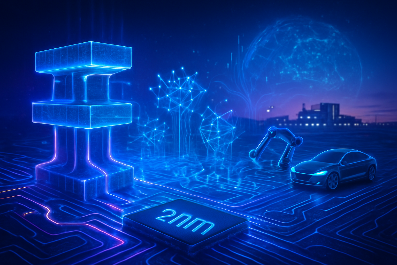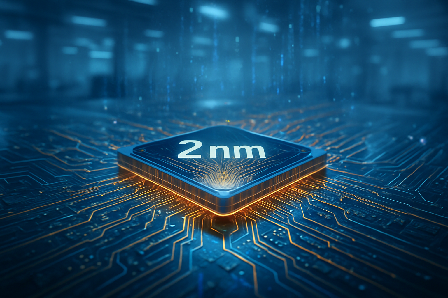
As the calendar turns to early 2026, the global semiconductor landscape has officially shifted on its axis. Taiwan Semiconductor Manufacturing Company (NYSE:TSM), commonly known as TSMC, has successfully crossed the finish line of its most ambitious technological transition in a decade. Following a rigorous ramp-up period that concluded in late 2025, the company’s 2nm (N2) node is now in high-volume manufacturing, ushering in the era of Gate-All-Around (GAA) nanosheet transistors. This milestone marks more than just a reduction in feature size; it represents the foundational infrastructure upon which the next generation of generative AI and high-performance computing (HPC) will be built.
The immediate significance of this development cannot be overstated. By moving into volume production ahead of its most optimistic competitors and maintaining superior yield rates, TSMC has effectively secured its position as the primary engine of the AI economy. With primary production hubs at Fab 22 in Kaohsiung and Fab 20 in Hsinchu reaching a combined output of over 50,000 wafers per month this January, the company is already churning out the silicon that will power the most advanced smartphones and data center accelerators of 2026 and 2027.
The Nanosheet Revolution: Engineering the Future of Silicon
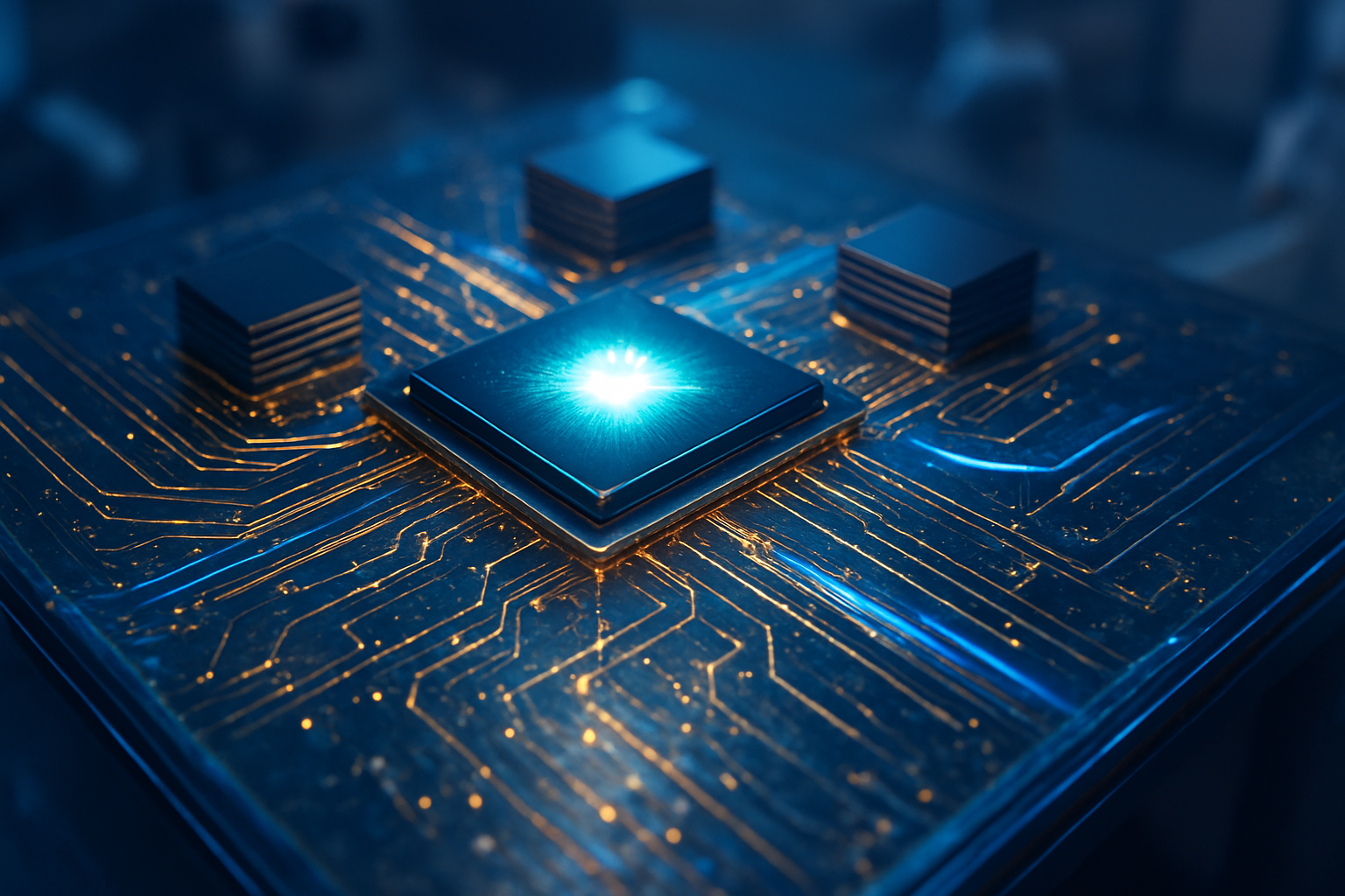
The N2 node represents a fundamental departure from the FinFET (Fin Field-Effect Transistor) architecture that has dominated the industry for the last several process generations. In traditional FinFETs, the gate controls the channel on three sides; however, as transistors shrink toward the 2nm threshold, current leakage becomes an insurmountable hurdle. TSMC’s shift to Gate-All-Around (GAA) nanosheet transistors solves this by wrapping the gate around all four sides of the channel, providing superior electrostatic control and drastically reducing power leakage.
Technical specifications for the N2 node are staggering. Compared to the previous 3nm (N3E) process, the 2nm node offers a 10% to 15% increase in performance at the same power envelope, or a significant 25% to 30% reduction in power consumption at the same clock speed. Furthermore, the N2 node introduces "Super High-Performance Metal-Insulator-Metal" (SHPMIM) capacitors. These components double the capacitance density while cutting resistance by 50%, a critical advancement for AI chips that must handle massive, instantaneous power draws without losing efficiency. Early logic test chips have reportedly achieved yield rates between 70% and 80%, a metric that validates TSMC's manufacturing prowess compared to the more volatile early yields seen in rival GAA implementations.
A High-Stakes Duel: Intel, Samsung, and the Battle for Foundry Supremacy
The successful ramp of N2 has profound implications for the competitive balance between the "Big Three" chipmakers. While Samsung Electronics (KRX:005930) was technically the first to move to GAA at the 3nm stage, its yields have historically struggled to compete with the stability of TSMC. Samsung’s recent launch of the SF2 node and the Exynos 2600 chip shows progress, but the company remains primarily a secondary source for major designers. Meanwhile, Intel (NASDAQ:INTC) has emerged as a formidable challenger with its 18A node. Intel’s 18A utilizes "PowerVia" (Backside Power Delivery), a technology TSMC will not integrate until its N2P variant in late 2026. This gives Intel a temporary technical lead in raw power delivery metrics, even as TSMC maintains a superior transistor density of roughly 313 million transistors per square millimeter.
For the world’s most valuable tech giants, the arrival of N2 is a strategic windfall. Apple (NASDAQ:AAPL), acting as TSMC’s "alpha" customer, has reportedly secured over 50% of the initial 2nm capacity to power its upcoming iPhone 18 series and the M5/M6 Mac silicon. Close on their heels is Nvidia (NASDAQ:NVDA), which is leveraging the N2 node for its next-generation AI platforms succeeding the Blackwell architecture. Other major players including Advanced Micro Devices (NASDAQ:AMD), Broadcom (NASDAQ:AVGO), and MediaTek (TPE:2454) have already finalized their 2026 production slots, signaling a collective industry bet that TSMC’s N2 will be the gold standard for efficiency and scale.
Scaling AI: The Broader Landscape of 2nm Integration
The transition to 2nm is inextricably linked to the trajectory of artificial intelligence. As Large Language Models (LLMs) grow in complexity, the demand for "compute" has become the defining constraint of the tech industry. The 25-30% power savings offered by N2 are not merely a luxury for mobile devices; they are a survival necessity for data centers. By reducing the energy required per inference or training cycle, 2nm chips allow hyperscalers like Microsoft (NASDAQ:MSFT) and Amazon (NASDAQ:AMZN) to pack more density into their existing power footprints, potentially slowing the skyrocketing environmental costs of the AI boom.
This milestone also reinforces the "Moore's Law is not dead" narrative, albeit with a caveat: while transistor density continues to increase, the cost per transistor is rising. The complexity of GAA manufacturing requires multi-billion dollar investments in Extreme Ultraviolet (EUV) lithography and specialized cleanrooms. This creates a widening "innovation gap" where only the largest, most capitalized companies can afford the leap to 2nm, potentially consolidating power within a handful of AI leaders while leaving smaller startups to rely on older, less efficient silicon.
The Roadmap Beyond: A16 and the 1.6nm Frontier
The arrival of 2nm mass production is just the beginning of a rapid-fire roadmap. TSMC has already disclosed that its N2P node—the enhanced version of 2nm featuring Backside Power Delivery—is on track for mass production in late 2026. This will be followed closely by the A16 node (1.6nm) in 2027, which will incorporate "Super PowerRail" technology to further optimize power distribution directly to the transistor's source and drain.
Experts predict that the next eighteen months will focus on "advanced packaging" as much as the nodes themselves. Technologies like CoWoS (Chip on Wafer on Substrate) will be essential to combine 2nm logic with high-bandwidth memory (HBM4) to create the massive AI "super-chips" of the future. The challenge moving forward will be heat dissipation; as transistors become more densely packed, managing the thermal output of these 2nm dies will require innovative liquid cooling and material science breakthroughs.
Conclusion: A Pivot Point for the Digital Age
TSMC’s successful transition to the 2nm N2 node in early 2026 stands as one of the most significant engineering feats of the decade. By navigating the transition from FinFET to GAA nanosheets while maintaining industry-leading yields, the company has solidified its role as the indispensable foundation of the AI era. While Intel and Samsung continue to provide meaningful competition, TSMC’s ability to scale this technology for giants like Apple and Nvidia ensures that the heartbeat of global innovation remains centered in Taiwan.
In the coming months, the industry will watch closely as the first 2nm consumer devices hit the shelves and the first N2-based AI clusters go online. This development is more than a technical upgrade; it is the starting gun for a new epoch of computing performance, one that will determine the pace of AI advancement for years to come.
This content is intended for informational purposes only and represents analysis of current AI developments.
TokenRing AI delivers enterprise-grade solutions for multi-agent AI workflow orchestration, AI-powered development tools, and seamless remote collaboration platforms.
For more information, visit https://www.tokenring.ai/.