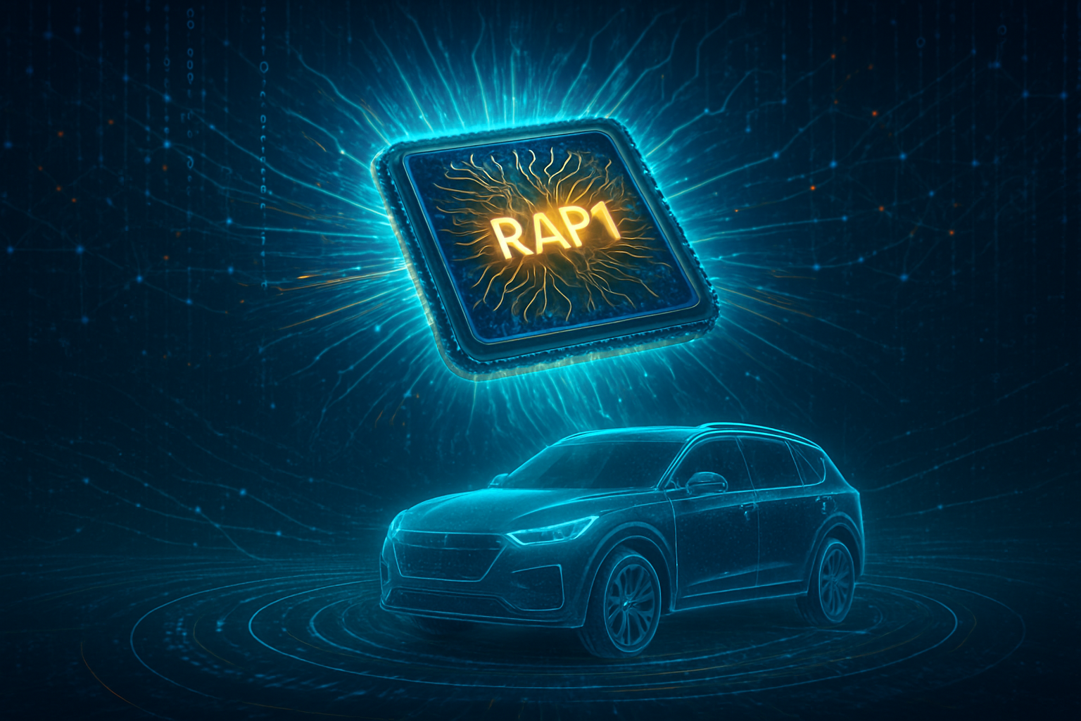
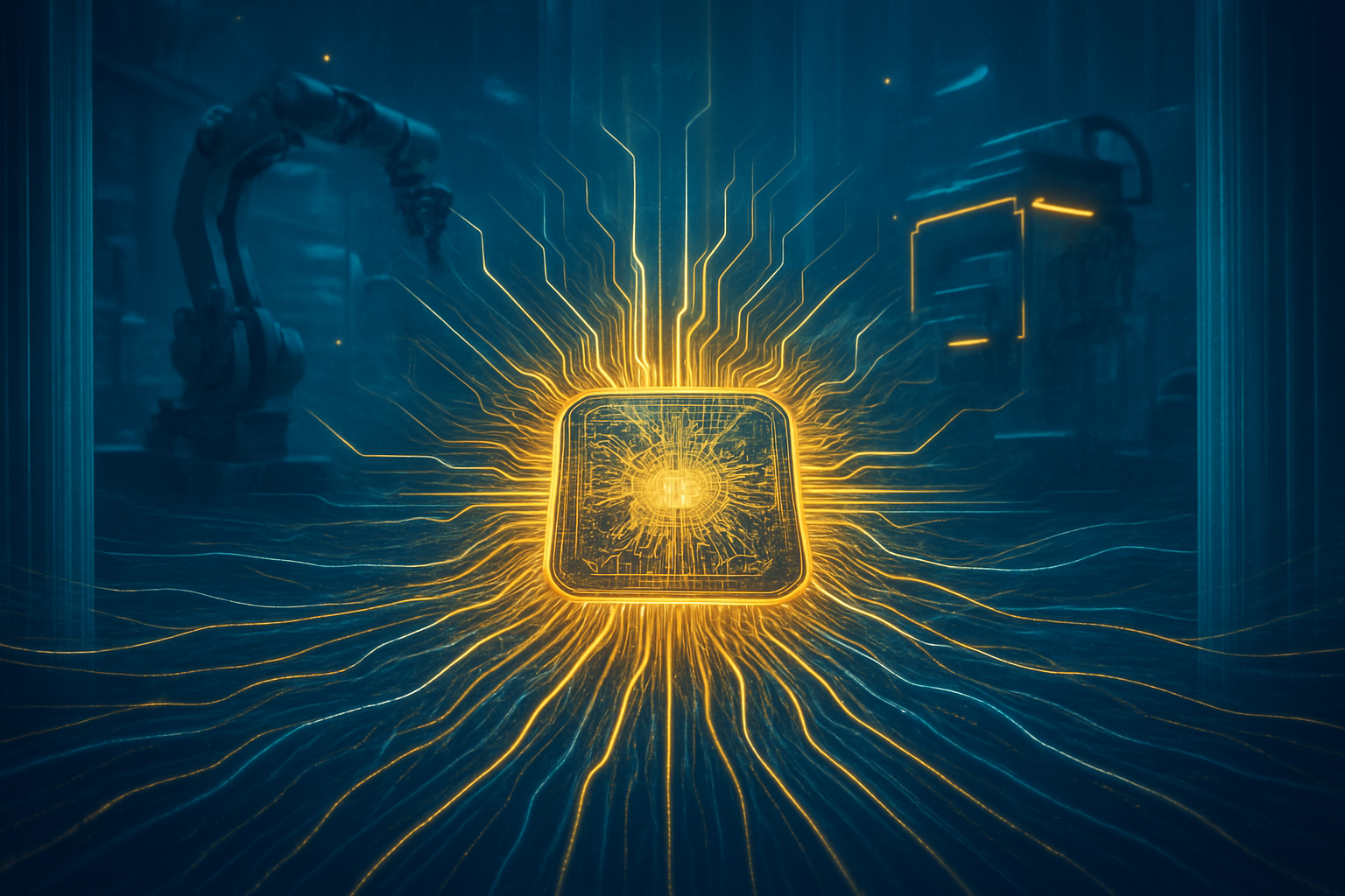
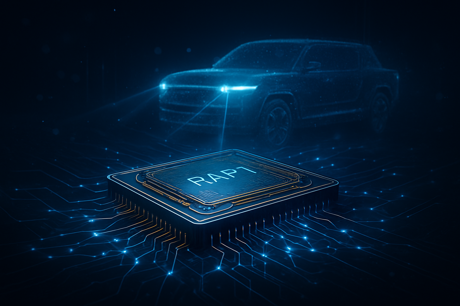
Tag: AI Chips

  • The Silicon Curtain Rises: Huawei’s Ascend 950 Series Achieves H100 Parity via ‘EUV-Refined’ Breakthroughs

    The Silicon Curtain Rises: Huawei’s Ascend 950 Series Achieves H100 Parity via ‘EUV-Refined’ Breakthroughs

    As of January 1, 2026, the global landscape of artificial intelligence hardware has undergone a seismic shift. Huawei has officially announced the wide-scale deployment of its Ascend 950 series AI processors, a milestone that signals the end of the West’s absolute monopoly on high-end compute. By leveraging a sophisticated "EUV-refined" manufacturing process and a vertically integrated stack, Huawei has achieved performance parity with the NVIDIA (NASDAQ: NVDA) H100 and H200 architectures, effectively neutralizing the impact of multi-year export restrictions.

    This development marks a pivotal moment in what Beijing terms "Internal Circulation"—a strategic pivot toward total technological self-reliance. The Ascend 950 is not merely a chip; it is the cornerstone of a parallel AI ecosystem. For the first time, Chinese hyperscalers and AI labs have access to domestic silicon that can train the world’s largest Large Language Models (LLMs) without relying on smuggled or depreciated hardware, fundamentally altering the geopolitical balance of the AI arms race.

    Technical Mastery: SAQP and the 'Mount Everest' Breakthrough

    The Ascend 950 series, specifically the 950PR (optimized for inference prefill) and the forthcoming 950DT (dedicated to heavy training), represents a triumph of engineering over constraint. While NVIDIA (NASDAQ: NVDA) utilizes TSMC’s (NYSE: TSM) advanced 4N and 3nm nodes, Huawei and its primary manufacturing partner, Semiconductor Manufacturing International Corporation (SMIC) (HKG: 0981), have achieved 5nm-class densities through a technique known as Self-Aligned Quadruple Patterning (SAQP). This "EUV-refined" process uses existing Deep Ultraviolet (DUV) lithography machines in complex, multi-pass configurations to etch circuits that were previously thought impossible without ASML’s (NASDAQ: ASML) restricted Extreme Ultraviolet (EUV) hardware.

    Specifications for the Ascend 950DT are formidable, boasting peak FP8 compute performance of up to 2.0 PetaFLOPS, placing it directly in competition with NVIDIA’s H200. To solve the "memory wall" that has plagued previous domestic chips, Huawei introduced HiZQ 2.0, a proprietary high-bandwidth memory solution that offers 4.0 TB/s of bandwidth, rivaling the HBM3e standards used in the West. This is paired with UnifiedBus, an interconnect fabric capable of 2.0 TB/s, which allows for the seamless clustering of thousands of NPUs into a single logical compute unit.

    Initial reactions from the AI research community have been a mix of astonishment and strategic recalibration. Researchers at organizations like DeepSeek and the Beijing Academy of Artificial Intelligence (BAAI) report that the Ascend 950, when paired with Huawei’s CANN 8.0 (Compute Architecture for Neural Networks) software, allows for one-line code conversions from CUDA-based models. This eliminates the "software moat" that has long protected NVIDIA, as the CANN 8.0 compiler can now automatically optimize kernels for the Ascend architecture with minimal performance loss.

    Reshaping the Global AI Market

    The arrival of the Ascend 950 series creates immediate winners within the Chinese tech sector. Tech giants like Baidu (NASDAQ: BIDU), Tencent (HKG: 0700), and Alibaba (NYSE: BABA) are expected to be the primary beneficiaries, as they can now scale their internal "Ernie" and "Tongyi Qianwen" models on stable, domestic supply chains. For these companies, the Ascend 950 represents more than just performance; it offers "sovereign certainty"—the guarantee that their AI roadmaps cannot be derailed by further changes in U.S. export policy.

    For NVIDIA (NASDAQ: NVDA), the implications are stark. While the company remains the global leader with its Blackwell and upcoming Rubin architectures, the "Silicon Curtain" has effectively closed off the world’s second-largest AI market. The competitive pressure is also mounting on other Western firms like Advanced Micro Devices (NASDAQ: AMD) and Intel (NASDAQ: INTC), who now face a Chinese market that is increasingly hostile to foreign silicon. Huawei’s ability to offer a full-stack solution—from the Kunpeng 950 CPUs to the Ascend NPUs and the OceanStor AI storage—positions it as a "one-stop shop" for national-scale AI infrastructure.

    Furthermore, the emergence of the Atlas 950 SuperPoD—a massive cluster housing 8,192 Ascend 950 chips—threatens to disrupt the global cloud compute market. Huawei claims this system delivers 6.7x the total computing power of current Western-designed clusters of similar scale. This strategic advantage allows Chinese startups to train models with trillions of parameters at a fraction of the cost previously incurred when renting "sanction-compliant" GPUs from international cloud providers.

    The Global Reshoring Perspective: A New Industrial Era

    From the perspective of China’s "Global Reshoring" strategy, the Ascend 950 is the ultimate proof of concept for industrial "Internal Circulation." While the West has focused on reshoring to secure jobs and supply chains, China’s version is an existential mandate to decouple from Western IP entirely. The success of the "EUV-refined" process suggests that the technological "ceiling" imposed by sanctions was more of a "hurdle" that Chinese engineers have now cleared through sheer iterative volume and state-backed capital.

    This shift mirrors previous industrial milestones, such as the development of China’s high-speed rail or its dominance in the EV battery market. It signifies a transition from a globalized, interdependent tech world to a bifurcated one. The "Silicon Curtain" is now a physical reality, with two distinct stacks of hardware, software, and standards. This raises significant concerns about global interoperability and the potential for a "cold war" in AI safety and alignment standards, as the two ecosystems may develop along radically different ethical and technical trajectories.

    Critics and skeptics point out that the "EUV-refined" DUV process is inherently less efficient, with lower yields and higher power consumption than true EUV manufacturing. However, in the context of national security and strategic autonomy, these economic inefficiencies are secondary to the primary goal of compute sovereignty. The Ascend 950 proves that a nation-state with sufficient resources can "brute-force" its way into the top tier of semiconductor design, regardless of international restrictions.

    The Horizon: 3nm and Beyond

    Looking ahead to the remainder of 2026 and 2027, Huawei’s roadmap shows no signs of slowing. Rumors of the Ascend 960 suggest that Huawei is already testing prototypes that utilize a fully domestic EUV lithography system developed under the secretive "Project Mount Everest." If successful, this would move China into the 3nm frontier by 2027, potentially reaching parity with NVIDIA’s next-generation architectures ahead of schedule.

    The next major challenge for the Ascend ecosystem will be the expansion of its developer base outside of China. While domestic adoption is guaranteed, Huawei is expected to aggressively market the Ascend 950 to "Global South" nations looking for an alternative to Western technology stacks. We can expect to see "AI Sovereignty" packages—bundled hardware, software, and training services—offered to countries in Southeast Asia, the Middle East, and Africa, further extending the reach of the Chinese AI ecosystem.

    A New Chapter in AI History

    The launch of the Ascend 950 series will likely be remembered as the moment the "unipolar" era of AI compute ended. Huawei has demonstrated that through a combination of custom silicon design, innovative manufacturing workarounds, and a massive vertically integrated stack, it is possible to rival the world’s most advanced technology firms under the most stringent constraints.

    Key takeaways from this development include the resilience of the Chinese semiconductor supply chain and the diminishing returns of export controls on mature-node and refined-node technologies. As we move into 2026, the industry must watch for the first benchmarks of LLMs trained entirely on Ascend 950 clusters. The performance of these models will be the final metric of success for Huawei’s ambitious leap into the future of AI.


    This content is intended for informational purposes only and represents analysis of current AI developments.

    TokenRing AI delivers enterprise-grade solutions for multi-agent AI workflow orchestration, AI-powered development tools, and seamless remote collaboration platforms.
    For more information, visit https://www.tokenring.ai/.

  • The Great Packaging Pivot: How TSMC is Doubling CoWoS Capacity to Break the AI Supply Bottleneck through 2026

    The Great Packaging Pivot: How TSMC is Doubling CoWoS Capacity to Break the AI Supply Bottleneck through 2026

    As of January 1, 2026, the global semiconductor landscape has undergone a fundamental shift. While the race for smaller nanometer nodes continues, the true front line of the artificial intelligence revolution has moved from the transistor to the package. Taiwan Semiconductor Manufacturing Company (TPE: 2330 / NYSE: TSM), the world’s largest contract chipmaker, is currently in the final stages of a massive multi-year expansion of its Chip-on-Wafer-on-Substrate (CoWoS) capacity. This strategic surge, aimed at doubling production annually through the end of 2026, represents the industry's most critical effort to resolve the persistent supply shortages that have hampered the AI sector since 2023.

    The immediate significance of this expansion cannot be overstated. For years, the primary constraint on the delivery of high-performance AI accelerators was not just the fabrication of the silicon dies themselves, but the complex "advanced packaging" required to connect those dies to High Bandwidth Memory (HBM). By scaling CoWoS capacity from approximately 35,000 wafers per month in late 2024 to a projected 130,000 wafers per month by the close of 2026, TSMC is effectively widening the narrowest pipe in the global technology supply chain, enabling the mass deployment of the next generation of generative AI models.

    The Technical Evolution: From CoWoS-S to the Era of CoWoS-L

    At the heart of TSMC’s expansion is a suite of advanced packaging technologies that go far beyond traditional methods. For the past decade, CoWoS-S (Silicon interposer) was the gold standard, using a monolithic silicon layer to link processors and memory. However, as AI chips like NVIDIA’s (NASDAQ: NVDA) Blackwell and the upcoming Rubin architectures grew in size and complexity, they began to exceed the "reticle limit"—the maximum size a single lithography step can print. To solve this, TSMC has pivoted toward CoWoS-L (LSI Bridge), which uses Local Silicon Interconnect (LSI) bridges to "stitch" multiple chiplets together. This allows for packages that are several times larger than previous generations, accommodating more compute power and significantly more HBM.

    To support this technical leap, TSMC has transformed its physical footprint in Taiwan. The company’s Advanced Packaging (AP) facilities have seen unprecedented investment. The AP6 facility in Zhunan, which became fully operational in late 2024, served as the initial catalyst for the capacity boost. However, the heavy lifting is now being handled by the AP8 facility in Tainan—a massive complex repurposed from a former display plant—and the burgeoning AP7 site in Chiayi. AP7 is planned to house up to eight production buildings, specifically designed to handle the intricate "stitching" required for CoWoS-L and the integration of System-on-Integrated-Chips (SoIC), which stacks chips vertically before they are placed on a substrate.

    Industry experts and the AI research community have reacted with cautious optimism. While the capacity increase is welcomed, the technical complexity of CoWoS-L introduces new manufacturing challenges, such as managing "warpage" (the physical bending of large packages during heat cycles) and ensuring signal integrity across massive interposers. Initial reports from early 2026 production runs suggest that TSMC has largely overcome these yield hurdles, though the precision required remains so high that advanced packaging is now considered as difficult and capital-intensive as the actual wafer fabrication process.

    The Market Scramble: NVIDIA, AMD, and the Rise of Custom ASICs

    The expansion of CoWoS capacity has profound implications for the competitive dynamics of the tech industry. NVIDIA remains the dominant force and the "anchor tenant" of TSMC’s packaging lines, reportedly securing over 60% of the total CoWoS capacity for 2025 and 2026. This preferential access has been a cornerstone of NVIDIA’s market lead, ensuring that as demand for its Blackwell and Rubin GPUs soared, it had the physical means to deliver them. For Advanced Micro Devices (NASDAQ: AMD), the expansion is equally vital. AMD’s Instinct MI350 and the upcoming MI400 series rely heavily on CoWoS-S and SoIC technologies to compete on memory bandwidth, and the increased supply from TSMC is the only way AMD can hope to gain market share in the enterprise AI space.

    Beyond the traditional chipmakers, a new class of competitors is benefiting from TSMC’s scale. Cloud Service Providers (CSPs) like Alphabet (NASDAQ: GOOGL), Amazon (NASDAQ: AMZN), and Meta (NASDAQ: META) are increasingly designing their own custom AI Application-Specific Integrated Circuits (ASICs). These companies are now competing directly with NVIDIA and AMD for TSMC’s packaging slots. By securing direct capacity, these tech giants can optimize their data centers for specific internal workloads, potentially disrupting the standard GPU market. The strategic advantage has shifted: in 2026, the company that wins is the one with the most guaranteed "wafer-per-month" allocations at TSMC’s AP7 and AP8 facilities.

    This massive capacity build-out also serves as a defensive moat for TSMC. While competitors like Intel (NASDAQ: INTC) and Samsung (KRX: 005930) are racing to develop their own advanced packaging solutions (such as Intel’s Foveros), TSMC’s sheer scale and proven yield rates for CoWoS-L have made it the nearly exclusive partner for high-end AI silicon. This concentration of power has solidified Taiwan’s role as the indispensable hub of the AI era, even as geopolitical concerns drive discussions about supply chain diversification.

    Beyond Moore’s Law: The "More than Moore" Significance

    The relentless expansion of CoWoS capacity is a clear signal that the semiconductor industry has entered the "More than Moore" era. For decades, progress was defined by shrinking transistors to fit more on a single chip. But as physical limits are reached and costs skyrocket, the industry has turned to "heterogeneous integration"—combining different types of chips (CPU, GPU, HBM) into a single, massive package. TSMC’s CoWoS is the physical manifestation of this trend, allowing for a level of performance that a single monolithic chip simply cannot achieve.

    This shift has wider socio-economic implications. The massive capital expenditure required for these packaging plants—often exceeding $10 billion per site—means that only the largest players can survive. This creates a barrier to entry that may lead to further consolidation in the semiconductor industry. Furthermore, the environmental impact of these facilities, which require immense amounts of power and ultra-pure water, has become a central topic of discussion in Taiwan. TSMC has responded by committing to more sustainable manufacturing processes, but the sheer scale of the 2026 capacity targets makes this a monumental challenge.

    Comparatively, this milestone is being viewed by historians as significant as the transition to EUV (Extreme Ultraviolet) lithography was a few years ago. Just as EUV was necessary to reach the 7nm and 5nm nodes, advanced packaging is now the "enabling technology" for the next decade of AI. Without it, the large language models (LLMs) and autonomous systems of the future would remain theoretical, trapped by the bandwidth limitations of traditional chip designs.

    The Next Frontier: Panel-Level Packaging and Glass Substrates

    Looking toward the latter half of 2026 and into 2027, the industry is already eyeing the next evolution: Fan-Out Panel-Level Packaging (FOPLP). While current CoWoS processes use round 12-inch wafers, FOPLP utilizes large rectangular panels. This transition, which TSMC is currently piloting at its Chiayi site, offers a significant leap in efficiency. Rectangular panels can fit more chips with less waste at the edges, potentially increasing the area utilization from 57% to over 80%. This will be essential as AI chips continue to grow in size, eventually reaching the point where even a 12-inch wafer is too small to be an efficient carrier.

    Another major development on the horizon is the adoption of glass substrates. Unlike the organic materials used today, glass offers superior flatness and thermal stability, which are critical for the ultra-fine circuitry required in future 2nm and 1.6nm AI processors. Experts predict that the first commercial applications of glass-based advanced packaging will appear by late 2027, further extending the performance gains of the CoWoS lineage. The challenge remains the extreme fragility of glass during the manufacturing process, a hurdle that TSMC’s R&D teams are working to solve as they finalize the 2026 expansion.

    Conclusion: A New Foundation for the AI Century

    TSMC’s aggressive expansion of CoWoS capacity through 2026 marks the end of the "packaging bottleneck" era and the beginning of a new phase of AI scaling. By doubling its output and mastering complex technologies like CoWoS-L and SoIC, TSMC has provided the physical foundation upon which the next generation of artificial intelligence will be built. The transition from 35,000 to over 110,000 wafers per month is not just a logistical achievement; it is a fundamental reconfiguration of how high-performance computers are designed and manufactured.

    As we move through 2026, the industry will be watching closely to see if TSMC can maintain its yield rates as it scales and whether competitors can finally mount a credible challenge to its packaging dominance. For now, the "Packaging War" has a clear leader. The long-term impact of this expansion will be felt in every sector touched by AI—from healthcare and autonomous transit to the very way we interact with technology. The bottleneck has been broken, and the race to fill that new capacity with even more powerful AI models has only just begun.


    This content is intended for informational purposes only and represents analysis of current AI developments.

    TokenRing AI delivers enterprise-grade solutions for multi-agent AI workflow orchestration, AI-powered development tools, and seamless remote collaboration platforms.
    For more information, visit https://www.tokenring.ai/.

  • Nvidia Solidifies AI Dominance with $20 Billion Strategic Acquisition of Groq’s LPU Technology

    Nvidia Solidifies AI Dominance with $20 Billion Strategic Acquisition of Groq’s LPU Technology

    In a move that has sent shockwaves through the semiconductor industry, Nvidia (NASDAQ: NVDA) announced on December 24, 2025, that it has entered into a definitive $20 billion agreement to acquire the core assets and intellectual property of Groq, the pioneer of the Language Processing Unit (LPU). The deal, structured as a massive asset purchase and licensing agreement to navigate an increasingly complex global regulatory environment, effectively integrates the world’s fastest AI inference technology into the Nvidia ecosystem. As part of the transaction, Groq founder and former Google TPU architect Jonathan Ross will join Nvidia to lead a new "Ultra-Low Latency" division, bringing the majority of Groq’s elite engineering team with him.

    The acquisition marks a pivotal shift in Nvidia's strategy as the AI market transitions from a focus on model training to a focus on real-time inference. By securing Groq’s deterministic architecture, Nvidia aims to eliminate the "memory wall" that has long plagued traditional GPU designs. This $20 billion bet is not merely about adding another chip to the catalog; it is a fundamental architectural evolution intended to consolidate Nvidia’s lead as the "AI Factory" for the world, ensuring that the next generation of generative AI applications—from humanoid robots to real-time translation—runs exclusively on Nvidia-powered silicon.

    The Death of Latency: Groq’s Deterministic Edge

    At the heart of this acquisition is Groq’s revolutionary LPU technology, which departs fundamentally from the probabilistic nature of traditional GPUs. While Nvidia’s current Blackwell architecture relies on complex scheduling, caches, and High Bandwidth Memory (HBM) to manage data, Groq’s LPU is entirely deterministic. The hardware is designed so that the compiler knows exactly where every piece of data is and what every transistor will be doing at every clock cycle. This eliminates the "jitter" and processing stalls common in multi-tenant GPU environments, allowing for the consistent, "speed-of-light" token generation that has made Groq a favorite among developers of real-time agents.

    Technically, the LPU’s greatest advantage lies in its use of massive on-chip SRAM (Static Random Access Memory) rather than the external HBM3e used by competitors. This configuration allows for internal memory bandwidth of up to 80 TB/s—roughly ten times faster than the top-tier chips from Advanced Micro Devices (NASDAQ: AMD) or Intel (NASDAQ: INTC). In benchmarks released earlier this year, Groq’s hardware achieved inference speeds of over 500 tokens per second for Llama 3 70B, a feat that typically requires a massive cluster of GPUs to replicate. By bringing this IP in-house, Nvidia can now solve the "Batch Size 1" problem, delivering near-instantaneous responses for individual user queries without the latency penalties inherent in traditional parallel processing.

    The initial reaction from the AI research community has been a mix of awe and apprehension. Experts note that while the integration of LPU technology will lead to unprecedented performance gains, it also signals the end of the "inference wars" that had briefly allowed smaller players to challenge Nvidia’s supremacy. "Nvidia just bought the one thing they didn't already have: the fastest short-burst inference engine on the planet," noted one lead analyst at a top Silicon Valley research firm. The move is seen as a direct response to the rising demand for "agentic AI," where models must think and respond in milliseconds to be useful in real-world interactions.

    Neutralizing the Competition: A Masterstroke in Market Positioning

    The competitive implications of this deal are devastating for Nvidia’s rivals. For years, AMD and Intel have attempted to carve out a niche in the inference market by offering high-memory GPUs as a more cost-effective alternative to Nvidia’s training-focused H100s and B200s. With the acquisition of Groq’s LPU technology, Nvidia has effectively closed that window. By integrating LPU logic into its upcoming Rubin architecture, Nvidia will be able to offer a hybrid "Superchip" that handles both massive-scale training and ultra-fast inference, leaving competitors with general-purpose architectures in a difficult position.

    The deal also complicates the "make-vs-buy" calculus for hyperscalers like Amazon (NASDAQ: AMZN), Microsoft (NASDAQ: MSFT), and Alphabet (NASDAQ: GOOGL). These tech giants have invested billions into custom silicon like AWS Inferentia and Google’s TPU to reduce their reliance on Nvidia. However, Groq was the only independent provider whose performance could consistently beat these internal chips. By absorbing Groq’s talent and tech, Nvidia has ensured that the "merchant" silicon available on the market remains superior to the proprietary chips developed by the cloud providers, potentially stalling further investment in custom internal hardware.

    For AI hardware startups like Cerebras and SambaNova, the $20 billion price tag sets an intimidating benchmark. These companies, which once positioned themselves as "Nvidia killers," now face a consolidated giant that possesses both the manufacturing scale of a trillion-dollar leader and the specialized architecture of a disruptive startup. Analysts suggest that the "exit path" for other hardware startups has effectively been choked, as few companies besides Nvidia have the capital or the strategic need to make a similar multi-billion-dollar acquisition in the current high-interest-rate environment.

    The Shift to Inference: Reshaping the AI Landscape

    This acquisition reflects a broader trend in the AI landscape: the transition from the "Build Phase" to the "Deployment Phase." In 2023 and 2024, the industry's primary bottleneck was training capacity. As we enter 2026, the bottleneck has shifted to the cost and speed of running these models at scale. Nvidia’s pivot toward LPU technology signals that the company views inference as the primary battlefield for the next five years. By owning the technology that defines the "speed of thought" for AI, Nvidia is positioning itself as the indispensable foundation for the burgeoning agentic economy.

    However, the deal is not without its concerns. Critics point to the "license-and-acquihire" structure of the deal—similar to Microsoft's 2024 deal with Inflection AI—as a strategic move to bypass antitrust regulators. By leaving the corporate shell of Groq intact to operate its "GroqCloud" service while hollowing out its engineering core and IP, Nvidia may avoid a full-scale merger review. This has raised red flags among digital rights advocates and smaller AI labs who fear that Nvidia’s total control over the hardware stack will lead to a "closed loop" where only those who pay Nvidia’s premium can access the fastest models.

    Comparatively, this milestone is being likened to Nvidia’s 2019 acquisition of Mellanox, which gave the company control over high-speed networking (InfiniBand). Just as Mellanox allowed Nvidia to build "data-center-scale" computers, the Groq acquisition allows them to build "real-time-scale" intelligence. It marks the moment when AI hardware moved beyond simply being "fast" to being "interactive," a requirement for the next generation of humanoid robotics and autonomous systems.

    The Road to Rubin: What Comes Next

    Looking ahead, the integration of Groq’s LPU technology will be the cornerstone of Nvidia’s future product roadmap. While the current Blackwell architecture will see immediate software-level optimizations based on Groq’s compiler tech, the true fusion will arrive with the Vera Rubin architecture, slated for late 2026. Internal reports suggest the development of a "Rubin CPX" chip—a specialized inference die that uses LPU-derived deterministic logic to handle the "prefill" phase of LLM processing, which is currently the most compute-intensive part of any user interaction.

    The most exciting near-term application for this technology is Project GR00T, Nvidia’s foundation model for humanoid robots. For a robot to operate safely in a human environment, it requires sub-100ms latency to process visual data and react to physical stimuli. The LPU’s deterministic performance is uniquely suited for these "hard real-time" requirements. Experts predict that by 2027, we will see the first generation of consumer-grade robots powered by hybrid GPU-LPU chips, capable of fluid, natural interaction that was previously impossible due to the lag inherent in cloud-based inference.

    Despite the promise, challenges remain. Integrating Groq’s SRAM-heavy design with Nvidia’s HBM-heavy GPUs will require a masterclass in chiplet packaging and thermal management. Furthermore, Nvidia must convince the developer community to adopt new compiler workflows to take full advantage of the LPU’s deterministic features. However, given Nvidia’s track record with CUDA, most industry observers expect the transition to be swift, further entrenching Nvidia’s software-hardware lock-in.

    A New Era for Artificial Intelligence

    The $20 billion acquisition of Groq is more than a business transaction; it is a declaration of intent. By absorbing its fastest competitor, Nvidia has moved to solve the most significant technical hurdle facing AI today: the latency gap. This deal ensures that as AI models become more complex and integrated into our daily lives, the hardware powering them will be able to keep pace with the speed of human thought. It is a definitive moment in AI history, marking the end of the era of "batch processing" and the beginning of the era of "instantaneous intelligence."

    In the coming weeks, the industry will be watching closely for the first "Groq-powered" updates to the Nvidia AI Enterprise software suite. As the engineering teams merge, the focus will shift to how quickly Nvidia can roll out LPU-enhanced inference nodes to its global network of data centers. For competitors, the message is clear: the bar for AI hardware has just been raised to a level that few, if any, can reach. As we move into 2026, the question is no longer who can build the biggest model, but who can make that model respond the fastest—and for now, the answer is unequivocally Nvidia.


    This content is intended for informational purposes only and represents analysis of current AI developments.

    TokenRing AI delivers enterprise-grade solutions for multi-agent AI workflow orchestration, AI-powered development tools, and seamless remote collaboration platforms.
    For more information, visit https://www.tokenring.ai/.

  • NVIDIA’s $20 Billion Groq Deal: A Strategic Strike for AI Inference Dominance

    NVIDIA’s $20 Billion Groq Deal: A Strategic Strike for AI Inference Dominance

    In a move that has sent shockwaves through Silicon Valley and the global semiconductor industry, NVIDIA (NASDAQ: NVDA) has finalized a blockbuster $20 billion agreement to license the intellectual property of AI chip innovator Groq and transition the vast majority of its engineering talent into the NVIDIA fold. The deal, structured as a strategic "license-and-acquihire," represents the largest single investment in NVIDIA’s history and marks a decisive pivot toward securing total dominance in the rapidly accelerating AI inference market.

    The centerpiece of the agreement is the integration of Groq’s ultra-low-latency Language Processing Unit (LPU) technology and the appointment of Groq founder and Tensor Processing Unit (TPU) inventor Jonathan Ross to a senior leadership role within NVIDIA. By absorbing the team and technology that many analysts considered the most credible threat to its hardware hegemony, NVIDIA is effectively skipping years of research and development. This strategic strike not only neutralizes a potent rival but also positions NVIDIA to own the "real-time" AI era, where speed and efficiency in running models are becoming as critical as the power used to train them.

    The LPU Advantage: Redefining AI Performance

    At the heart of this deal is Groq’s revolutionary LPU architecture, which differs fundamentally from the traditional Graphics Processing Units (GPUs) that have powered the AI boom to date. While GPUs are masters of parallel processing—handling thousands of small tasks simultaneously—they often struggle with the sequential nature of Large Language Models (LLMs), leading to "jitter" or variable latency. In contrast, the LPU utilizes a deterministic, single-core architecture. This design allows the system to know exactly where data is at any given nanosecond, resulting in predictable, sub-millisecond response times that are essential for fluid, human-like AI interactions.

    Technically, the LPU’s secret weapon is its reliance on massive on-chip SRAM (Static Random-Access Memory) rather than the High Bandwidth Memory (HBM) used by NVIDIA’s current H100 and B200 chips. By keeping data directly on the processor, the LPU achieves a memory bandwidth of up to 80 terabytes per second—nearly ten times that of existing high-end GPUs. This architecture excels at "Batch Size 1" processing, meaning it can generate tokens for a single user instantly without needing to wait for other requests to bundle together. For the AI research community, this is a game-changer; it enables "instantaneous" reasoning in models like GPT-5 and Claude 4, which were previously bottlenecked by the physical limits of HBM data transfer.

    Industry experts have reacted to the news with a mix of awe and caution. "NVIDIA just bought the fastest lane on the AI highway," noted one lead analyst at a major tech research firm. "By bringing Jonathan Ross—the man who essentially invented the modern AI chip at Google—into their ranks, NVIDIA isn't just buying hardware; they are buying the architectural blueprint for the next decade of computing."

    Reshaping the Competitive Landscape

    The strategic implications for the broader tech industry are profound. For years, major cloud providers and competitors like Alphabet Inc. (NASDAQ: GOOGL) and Advanced Micro Devices, Inc. (NASDAQ: AMD) have been racing to develop specialized inference ASICs (Application-Specific Integrated Circuits) to chip away at NVIDIA’s market share. Google’s TPU and Amazon’s Inferentia were designed specifically to offer a cheaper, faster alternative to NVIDIA’s general-purpose GPUs. By licensing Groq’s LPU technology, NVIDIA has effectively leapfrogged these custom solutions, offering a commercial product that matches or exceeds the performance of in-house hyperscaler silicon.

    This deal creates a significant hurdle for other AI chip startups, such as Cerebras and Sambanova, who now face a competitor that possesses both the massive scale of NVIDIA and the specialized speed of Groq. Furthermore, the "license-and-acquihire" structure allows NVIDIA to avoid some of the regulatory scrutiny that would accompany a full acquisition. Because Groq will continue to exist as an independent entity operating its "GroqCloud" service, NVIDIA can argue it is fostering an ecosystem rather than absorbing it, even as it integrates Groq’s core innovations into its own future product lines.

    For major AI labs like OpenAI and Anthropic, the benefit is immediate. Access to LPU-integrated NVIDIA hardware means they can deploy "agentic" AI—autonomous systems that can think, plan, and react in real-time—at a fraction of the current latency and power cost. This move solidifies NVIDIA’s position as the indispensable backbone of the AI economy, moving them from being the "trainers" of AI to the "engine" that runs it every second of the day.

    From Training to Inference: The Great AI Shift

    The $20 billion price tag reflects a broader trend in the AI landscape: the shift from the "Training Era" to the "Inference Era." While the last three years were defined by the massive clusters of GPUs needed to build models, the next decade will be defined by the trillions of queries those models must answer. Analysts predict that by 2030, the market for AI inference will be ten times larger than the market for training. NVIDIA’s move is a preemptive strike to ensure that as the industry evolves, its revenue doesn't peak with the completion of the world's largest data centers.

    This acquisition draws parallels to NVIDIA’s 2020 purchase of Mellanox, which gave the company control over the high-speed networking (InfiniBand) necessary for massive GPU clusters. Just as Mellanox allowed NVIDIA to dominate training at scale, Groq’s technology will allow them to dominate inference at speed. However, this milestone is perhaps even more significant because it addresses the growing concern over AI's energy consumption. The LPU architecture is significantly more power-efficient for inference tasks than traditional GPUs, providing a path toward sustainable AI scaling as global power grids face increasing pressure.

    Despite the excitement, the deal is not without its critics. Some in the open-source community express concern that NVIDIA’s tightening grip on both training and inference hardware could lead to a "black box" ecosystem where the most efficient AI can only run on proprietary NVIDIA stacks. This concentration of power in a single company’s hands remains a focal point for regulators in the US and EU, who are increasingly wary of "killer acquisitions" in the semiconductor space.

    The Road Ahead: Real-Time Agents and "Vera Rubin"

    Looking toward the near-term future, the first fruits of this deal are expected to appear in NVIDIA’s 2026 hardware roadmap, specifically the rumored "Vera Rubin" architecture. Industry insiders suggest that NVIDIA will integrate LPU-derived "inference blocks" directly onto its next-generation dies, creating a hybrid chip capable of switching between heavy-lift training and ultra-fast inference seamlessly. This would allow a single server rack to handle the entire lifecycle of an AI model with unprecedented efficiency.

    The most transformative applications will likely be in the realm of real-time AI agents. With the latency barriers removed, we can expect to see the rise of voice assistants that have zero "thinking" delay, real-time language translation that feels natural, and autonomous systems in robotics and manufacturing that can process visual data and make decisions in microseconds. The challenge for NVIDIA will be the complex task of merging Groq’s software-defined hardware approach with its own CUDA software stack, a feat of engineering that Jonathan Ross is uniquely qualified to lead.

    Experts predict that the coming months will see a flurry of activity as NVIDIA's partners, including Microsoft Corp. (NASDAQ: MSFT) and Meta, scramble to secure early access to the first LPU-enhanced systems. The "race to zero latency" has officially begun, and with this $20 billion move, NVIDIA has claimed the pole position.

    A New Chapter in the AI Revolution

    NVIDIA’s licensing of Groq’s IP and the absorption of its engineering core represents a watershed moment in the history of computing. It is a clear signal that the "GPU-only" era of AI is evolving into a more specialized, diverse hardware landscape. By successfully identifying and integrating the most advanced inference technology on the market, NVIDIA has once again demonstrated the strategic agility that has made it one of the most valuable companies in the world.

    The key takeaway for the industry is that the battle for AI supremacy has moved beyond who can build the largest model to who can deliver that model’s intelligence the fastest. As we look toward 2026, the integration of Groq’s deterministic architecture into the NVIDIA ecosystem will likely be remembered as the move that made real-time, ubiquitous AI a reality.

    In the coming weeks, all eyes will be on the first joint technical briefings from NVIDIA and the former Groq team. As the dust settles on this $20 billion deal, the message to the rest of the industry is clear: NVIDIA is no longer just a chip company; it is the architect of the real-time intelligent world.


    This content is intended for informational purposes only and represents analysis of current AI developments.

    TokenRing AI delivers enterprise-grade solutions for multi-agent AI workflow orchestration, AI-powered development tools, and seamless remote collaboration platforms.
    For more information, visit https://www.tokenring.ai/.

  • Nvidia’s $20 Billion Strategic Gambit: Acquihiring Groq to Define the Era of Real-Time Inference

    Nvidia’s $20 Billion Strategic Gambit: Acquihiring Groq to Define the Era of Real-Time Inference

    In a move that has sent shockwaves through the semiconductor industry, NVIDIA (NASDAQ: NVDA) has finalized a landmark $20 billion "license-and-acquihire" deal with the high-speed AI chip startup Groq. Announced in late December 2025, the transaction represents Nvidia’s largest strategic maneuver since its failed bid for Arm, signaling a definitive shift in the company’s focus from the heavy lifting of AI training to the lightning-fast world of real-time AI inference. By absorbing the leadership and core intellectual property of the company that pioneered the Language Processing Unit (LPU), Nvidia is positioning itself to own the entire lifecycle of the "AI Factory."

    The deal is structured to navigate an increasingly complex regulatory landscape, utilizing a "reverse acqui-hire" model that brings Groq’s visionary founders, Jonathan Ross and Sunny Madra, directly into Nvidia’s executive ranks while securing long-term licensing for Groq’s deterministic hardware architecture. As the industry moves away from static chatbots and toward "agentic AI"—autonomous systems that must reason and act in milliseconds—Nvidia’s integration of LPU technology effectively closes the performance gap that specialized ASICs (Application-Specific Integrated Circuits) had begun to exploit.

    The LPU Integration: Solving the "Memory Wall" for the Vera Rubin Era

    At the heart of this $20 billion deal is Groq’s proprietary LPU technology, which Nvidia plans to integrate into its upcoming "Vera Rubin" architecture, slated for a 2026 rollout. Unlike traditional GPUs that rely heavily on High Bandwidth Memory (HBM)—a component that has faced persistent supply shortages and high power costs—Groq’s LPU utilizes on-chip SRAM. This technical pivot allows for "Batch Size 1" processing, enabling the generation of thousands of tokens per second for a single user without the latency penalties associated with data movement in traditional architectures.

    Industry experts note that this integration addresses the "Memory Wall," a long-standing bottleneck where processor speeds outpace the ability of memory to deliver data. By incorporating Groq’s deterministic software stack, which predicts exact execution times for AI workloads, Nvidia’s next-generation "AI Factories" will be able to offer unprecedented reliability for mission-critical applications. Initial benchmarks suggest that LPU-enhanced Nvidia systems could be up to 10 times more energy-efficient per token than current H100 or B200 configurations, a critical factor as global data center power consumption reaches a tipping point.

    Strengthening the Moat: Competitive Fallout and Market Realignment

    The move is a strategic masterstroke that complicates the roadmap for Nvidia’s primary rivals, including Advanced Micro Devices (NASDAQ: AMD) and Intel (NASDAQ: INTC), as well as cloud-native chip efforts from Alphabet (NASDAQ: GOOGL) and Amazon (NASDAQ: AMZN). By bringing Jonathan Ross—the original architect of Google’s TPU—into the fold as Nvidia’s new Chief Software Architect, CEO Jensen Huang has effectively neutralized one of his most formidable intellectual competitors. Sunny Madra, who joins as VP of Hardware, is expected to spearhead the effort to make LPU technology "invisible" to developers by absorbing it into the existing CUDA ecosystem.

    For the broader startup ecosystem, the deal is a double-edged sword. While it validates the massive valuations of specialized AI silicon companies, it also demonstrates Nvidia’s willingness to spend aggressively to maintain its ~90% market share. Startups focusing on inference-only hardware now face a competitor that possesses both the industry-standard software stack and the most advanced low-latency hardware IP. Analysts suggest that this "license-and-acquihire" structure may become the new blueprint for Big Tech acquisitions, allowing giants to bypass traditional antitrust blocks while still securing the talent and tech they need to stay ahead.

    Beyond GPUs: The Rise of the Hybrid AI Factory

    The significance of this deal extends far beyond a simple hardware upgrade; it represents the maturation of the AI landscape. In 2023 and 2024, the industry was obsessed with training larger and more capable models. By late 2025, the focus has shifted entirely to inference—the actual deployment and usage of these models in the real world. Nvidia’s "AI Factory" vision now includes a hybrid silicon approach: GPUs for massive parallel training and LPU-derived cores for instantaneous, agentic reasoning.

    This shift mirrors previous milestones in computing history, such as the transition from general-purpose CPUs to specialized graphics accelerators in the 1990s. By internalizing the LPU, Nvidia is acknowledging that the "one-size-fits-all" GPU era is evolving. There are, however, concerns regarding market consolidation. With Nvidia controlling both the training and the most efficient inference hardware, the "CUDA Moat" has become more of a "CUDA Fortress," raising questions about long-term pricing power and the ability of smaller players to compete without Nvidia’s blessing.

    The Road to 2026: Agentic AI and Autonomous Systems

    Looking ahead, the immediate priority for the newly combined teams will be the release of updated TensorRT and Triton libraries. These software updates are expected to allow existing AI models to run on LPU-enhanced hardware with zero code changes, a move that would facilitate an overnight performance boost for thousands of enterprise customers. Near-term applications are likely to focus on voice-to-voice translation, real-time financial trading algorithms, and autonomous robotics, all of which require the sub-100ms response times that the Groq-Nvidia hybrid architecture promises.

    However, challenges remain. Integrating two radically different hardware philosophies—the stochastic nature of traditional GPUs and the deterministic nature of LPUs—will require a massive engineering effort. Experts predict that the first "true" hybrid chip will not hit the market until the second half of 2026. Until then, Nvidia is expected to offer "Groq-powered" inference clusters within its DGX Cloud service, providing a playground for developers to optimize their agentic workflows.

    A New Chapter in the AI Arms Race

    The $20 billion deal for Groq marks the end of the "Inference Wars" of 2025, with Nvidia emerging as the clear victor. By securing the talent of Ross and Madra and the efficiency of the LPU, Nvidia has not only upgraded its hardware but has also de-risked its supply chain by moving away from a total reliance on HBM. This transaction will likely be remembered as the moment Nvidia transitioned from a chip company to the foundational infrastructure provider for the autonomous age.

    As we move into 2026, the industry will be watching closely to see how quickly the "Vera Rubin" architecture can deliver on its promises. For now, the message from Santa Clara is clear: Nvidia is no longer just building the brains that learn; it is building the nervous system that acts. The era of real-time, agentic AI has officially arrived, and it is powered by Nvidia.


    This content is intended for informational purposes only and represents analysis of current AI developments.

    TokenRing AI delivers enterprise-grade solutions for multi-agent AI workflow orchestration, AI-powered development tools, and seamless remote collaboration platforms.
    For more information, visit https://www.tokenring.ai/.

  • The 2nm Bottleneck: Apple Secures Lion’s Share of TSMC’s Next-Gen Capacity as Industry Braces for Scarcity

    The 2nm Bottleneck: Apple Secures Lion’s Share of TSMC’s Next-Gen Capacity as Industry Braces for Scarcity

    As 2025 draws to a close, the semiconductor industry is entering a period of unprecedented supply-side tension. Taiwan Semiconductor Manufacturing Company (NYSE: TSM) has officially signaled a "capacity crunch" for its upcoming 2nm (N2) process node, revealing that production slots are effectively sold out through the end of 2026. In a move that mirrors its previous dominance of the 3nm node, Apple (NASDAQ: AAPL) has reportedly secured over 50% of the initial 2nm volume, leaving a roster of high-performance computing (HPC) giants and mobile competitors to fight for the remaining fabrication windows.

    This scarcity marks a critical juncture for the artificial intelligence and consumer electronics sectors. With the first 2nm-powered devices expected to hit the market in late 2026, the bottleneck at TSMC is no longer just a manufacturing hurdle—it is a strategic gatekeeper. For companies like NVIDIA (NASDAQ: NVDA) and AMD (NASDAQ: AMD), the limited availability of 2nm wafers is forcing a recalibration of product roadmaps, as the industry grapples with the escalating costs and technical complexities of the most advanced silicon on the planet.

    The N2 Leap: GAAFET and the End of the FinFET Era

    The transition to the N2 node represents TSMC’s most significant architectural shift in over a decade. After years of refining the FinFET (Fin Field-Effect Transistor) structure, the foundry is officially moving to Gate-All-Around FET (GAAFET) technology, specifically utilizing a nanosheet architecture. In this design, the gate surrounds the channel on all four sides, providing vastly superior electrostatic control. This technical pivot is essential for maintaining the pace of Moore’s Law, as it significantly reduces current leakage—a primary obstacle in the sub-3nm era.

    Technically, the N2 node delivers substantial gains over the current N3E (3nm) standard. Early performance metrics indicate a 10–15% speed improvement at the same power levels, or a 25–30% reduction in power consumption at the same clock speeds. Furthermore, transistor density is expected to increase by approximately 1.1x. However, this first generation of 2nm will not yet include "Backside Power Delivery"—a feature TSMC calls the "Super Power Rail." That innovation is reserved for the N2P and A16 (1.6nm) nodes, which are slated for late 2026 and 2027, respectively.

    Initial reactions from the semiconductor research community have been a mix of awe and caution. While the efficiency gains of GAAFET are undeniable, the cost of entry has reached a fever pitch. Reports suggest that 2nm wafers are priced at approximately $30,000 per unit—a 50% premium over 3nm wafers. Industry experts note that while Apple can absorb these costs by positioning its A20 and M6 chips as premium offerings, smaller players may find the financial barrier to 2nm entry nearly insurmountable, potentially widening the gap between the "silicon elite" and the rest of the market.

    The Capacity War: Apple’s Dominance and the Ripple Effect

    Apple’s aggressive booking of over half of TSMC’s 2nm capacity for 2026 serves as a defensive moat against its competitors. By locking down the A20 chip production for the iPhone 18 series, Apple ensures it will be the first to offer consumer-grade 2nm hardware. This strategy also extends to its Mac and Vision Pro lines, with the M6 and R2 chips expected to utilize the same N2 capacity. This "buyout" strategy forces other tech giants to scramble for what remains, creating a high-stakes queue that favors those with the deepest pockets.

    The implications for the AI hardware market are particularly profound. NVIDIA, which has been the primary beneficiary of the AI boom, has reportedly had to adjust its "Rubin" GPU architecture plans. While the highest-end variants of the Rubin Ultra may eventually see 2nm production, the bulk of the initial Rubin (R100) volume is expected to remain on refined 3nm nodes due to the 2nm supply constraints. Similarly, AMD is facing a tight window for its Zen 6 "Venice" processors; while AMD was among the first to tape out 2nm designs, its ability to scale those products in 2026 will be severely limited by Apple’s massive footprint at TSMC’s Hsinchu and Kaohsiung fabs.

    This crunch has led to a renewed interest in secondary sourcing. Both AMD and Google (NASDAQ: GOOGL) are reportedly evaluating Samsung’s (KRX: 005930) 2nm (SF2) process as a potential alternative. However, yield concerns continue to plague Samsung, leaving TSMC as the only reliable provider for high-volume, leading-edge silicon. For startups and mid-sized AI labs, the 2nm crunch means that access to the most efficient "AI at the edge" hardware will be delayed, potentially slowing the deployment of sophisticated on-device AI models that require the power-per-watt efficiency only 2nm can provide.

    Silicon Geopolitics and the AI Landscape

    The 2nm capacity crunch is more than a supply chain issue; it is a reflection of the broader AI landscape's insatiable demand for compute. As AI models migrate from massive data centers to local devices—a trend often referred to as "Edge AI"—the efficiency of the underlying silicon becomes the primary differentiator. The N2 node is the first process designed from the ground up to support the power envelopes required for running multi-billion parameter models on smartphones and laptops without devastating battery life.

    This development also highlights the increasing concentration of technological power. With TSMC remaining the sole provider of viable 2nm logic, the world’s most advanced AI and consumer tech roadmaps are tethered to a handful of square miles in Taiwan. While TSMC is expanding its Arizona (Fab 21) operations, high-volume 2nm production in the United States is not expected until at least 2027. This geographic concentration remains a point of concern for global supply chain resilience, especially as geopolitical tensions continue to simmer.

    Comparatively, the move to 2nm feels like the "Great 3nm Scramble" of 2023, but with higher stakes. In the previous cycle, the primary driver was traditional mobile performance. Today, the driver is the "AI PC" and "AI Phone" revolution. The ability to run generative AI locally is seen as the next major growth engine for the tech industry, and the 2nm node is the essential fuel for that engine. The fact that capacity is already booked through 2026 suggests that the industry expects the AI-driven upgrade cycle to be both long and aggressive.

    Looking Ahead: From N2 to the 1.4nm Frontier

    As TSMC ramps up its Fab 20 in Hsinchu and Fab 22 in Kaohsiung to meet the 2nm demand, the roadmap beyond 2026 is already taking shape. The near-term focus will be the introduction of N2P, which will integrate the much-anticipated Backside Power Delivery. This refinement is expected to offer an additional 5-10% performance boost by moving the power distribution network to the back of the wafer, freeing up more space for signal routing on the front.

    Looking further out, TSMC has already begun discussing the A14 (1.4nm) node, which is targeted for 2027 and 2028. This next frontier will likely involve High-NA (Numerical Aperture) EUV lithography, a technology that Intel (NASDAQ: INTC) has been aggressively pursuing to regain its "process leadership" crown. The competition between TSMC’s N2/A14 and Intel’s 18A/14A processes will define the next five years of semiconductor history, determining whether TSMC maintains its near-monopoly or if a more balanced ecosystem emerges.

    The immediate challenge for the industry, however, remains the 2026 capacity gap. Experts predict that we may see a "tiered" market emerge, where only the most expensive flagship devices utilize 2nm silicon, while "Pro" and standard models are increasingly stratified by process node rather than just feature sets. This could lead to a longer replacement cycle for mid-range devices, as the most meaningful performance leaps are reserved for the ultra-premium tier.

    Conclusion: A New Era of Scarcity

    The 2nm capacity crunch at TSMC is a stark reminder that even in an era of digital abundance, the physical foundations of technology are finite. Apple’s successful maneuver to secure the majority of N2 capacity for its A20 chips gives it a formidable lead in the "AI at the edge" race, but it leaves the rest of the industry in a precarious position. For the next 24 months, the story of AI will be written as much by manufacturing yields and wafer allocations as it will be by software breakthroughs.

    As we move into 2026, the primary metric to watch will be TSMC’s yield rates for the new GAAFET architecture. If the transition proves smoother than the difficult 3nm ramp, we may see additional capacity unlocked for secondary customers. However, if yields struggle, the "capacity crunch" could turn into a full-scale hardware drought, potentially delaying the next generation of AI-integrated products across the board. For now, the silicon world remains a game of musical chairs—and Apple has already claimed the best seats in the house.


    This content is intended for informational purposes only and represents analysis of current AI developments.

    TokenRing AI delivers enterprise-grade solutions for multi-agent AI workflow orchestration, AI-powered development tools, and seamless remote collaboration platforms.
    For more information, visit https://www.tokenring.ai/.

  • TSMC Secures $4.7B in Global Subsidies for Manufacturing Diversification Across US, Europe, and Asia

    TSMC Secures $4.7B in Global Subsidies for Manufacturing Diversification Across US, Europe, and Asia

    In a definitive move toward "semiconductor sovereignty," Taiwan Semiconductor Manufacturing Company (NYSE: TSM) has secured approximately $4.71 billion (NT$147 billion) in government subsidies over the past two years. This massive capital injection from the United States, Japan, Germany, and China marks a historic shift in the silicon landscape, as the world’s most advanced chipmaker aggressively diversifies its manufacturing footprint away from its home base in Taiwan.

    The funding is the primary engine behind TSMC’s multi-continent expansion, supporting the construction of high-tech "fabs" in Arizona, Kumamoto, and Dresden. As of December 26, 2025, this strategy has already yielded significant results, with the first Arizona facility entering mass production and achieving yield rates that rival or even exceed those of its Taiwanese counterparts. This global diversification is a direct response to escalating geopolitical tensions and the urgent need for resilient supply chains in an era where artificial intelligence (AI) has become the new "digital oil."

    Yielding Success: The Technical Triumph of the 'Silicon Desert'

    The technical centerpiece of TSMC’s expansion is its $65 billion investment in Arizona. As of late 2025, Fab 21 Phase 1 has officially entered mass production using 4nm and 5nm process technologies. In a development that has surprised many industry skeptics, internal reports indicate that the Arizona facility has achieved a landmark 92% yield rate—surpassing the yield of comparable facilities in Taiwan by approximately 4%. This technical milestone proves that TSMC can successfully export its highly guarded manufacturing "secret sauce" to Western soil without sacrificing efficiency.

    Beyond the initial 4nm success, TSMC is accelerating its roadmap for more advanced nodes. Construction on Phase 2 (3nm) is now complete, with equipment installation running ahead of schedule for a 2027 mass production target. Furthermore, the company broke ground on Phase 3 in April 2025, which is designated for the revolutionary "Angstrom-class" nodes (2nm and A16). This ensures that the most sophisticated AI processors of the next decade—those requiring extreme transistor density and power efficiency—will have a dedicated home in the United States.

    In Japan, the Kumamoto facility (JASM) has already transitioned to high-volume production for 12nm to 28nm specialty chips, focusing on the automotive and industrial sectors. However, responding to the "Giga Cycle" of AI demand, TSMC is reportedly considering a pivot for its second Japanese fab, potentially skipping 6nm to move directly into 4nm or 2nm production. Meanwhile, in Dresden, Germany, the ESMC facility has entered the main structural construction phase, aiming to become Europe’s first FinFET-capable foundry by 2027, securing the continent’s industrial IoT and automotive sovereignty.

    The AI Power Play: Strategic Advantages for Tech Giants

    This geographic diversification creates a massive strategic advantage for U.S.-based tech giants like Nvidia (NASDAQ: NVDA), Apple (NASDAQ: AAPL), and Advanced Micro Devices (NASDAQ: AMD). For years, these companies have faced the "Taiwan Risk"—the fear that a regional conflict or natural disaster could sever the world’s supply of high-end AI chips. By late 2025, that risk has been significantly de-risked. For the first time, Nvidia’s next-generation Blackwell and Rubin GPUs can be fabricated, tested, and packaged entirely within the United States.

    The market positioning of these companies is further strengthened by TSMC’s new partnership with Amkor Technology (NASDAQ: AMKR). By establishing advanced packaging capabilities in Arizona, TSMC has solved the "last mile" problem of chip manufacturing. Previously, even if a chip was made in the U.S., it often had to be sent back to Asia for sophisticated Chip-on-Wafer-on-Substrate (CoWoS) packaging. The localized ecosystem now allows for a complete, domestic AI hardware pipeline, providing a competitive moat for American hyperscalers who can now claim "Made in the USA" status for their AI infrastructure.

    While TSMC benefits from these subsidies, the competitive pressure on Intel (NASDAQ: INTC) has intensified. As the U.S. government moves toward more aggressive self-sufficiency targets—aiming for 40% domestic production by 2030—TSMC’s ability to deliver high yields on American soil poses a direct challenge to Intel’s "Foundry" ambitions. The subsidies have effectively leveled the playing field, allowing TSMC to offset the higher costs of operating in the U.S. and Europe while maintaining its technical lead.

    Semiconductor Sovereignty and the New Geopolitics of Silicon

    The $4.71 billion in subsidies represents more than just financial aid; it is the physical manifestation of "semiconductor sovereignty." Governments are no longer content to let market forces dictate the location of critical infrastructure. The U.S. CHIPS and Science Act and the EU Chips Act have transformed semiconductors into a matter of national security. This shift mirrors previous global milestones, such as the space race or the development of the interstate highway system, where state-funded infrastructure became the bedrock of future economic eras.

    However, this transition is not without friction. In China, TSMC’s Nanjing fab is facing a significant regulatory hurdle as the U.S. Department of Commerce is set to revoke its "Validated End User" (VEU) status on December 31, 2025. This move will end blanket approvals for U.S.-controlled tool shipments, forcing TSMC to navigate a complex licensing landscape to maintain its operations in the region. This development underscores the "bifurcation" of the global tech industry, where the West and East are increasingly building separate, non-overlapping supply chains.

    The broader AI landscape is also feeling the impact. The availability of regional "foundry clusters" means that AI startups and researchers can expect more stable pricing and shorter lead times for specialized silicon. The concentration of cutting-edge production is no longer a single point of failure in Taiwan, but a distributed network. While concerns remain about the long-term inflationary impact of fragmented supply chains, the immediate result is a more resilient foundation for the global AI revolution.

    The Road Ahead: 2nm and the Future of Edge AI

    Looking toward 2026 and 2027, the focus will shift from building factories to perfecting the next generation of "Angstrom-class" transistors. TSMC’s Arizona and Japan facilities are expected to be the primary sites for the rollout of 2nm technology, which will power the next wave of "Edge AI"—bringing sophisticated LLMs directly onto smartphones and wearable devices without relying on the cloud.

    The next major challenge for TSMC and its government partners will be talent acquisition and the development of a local workforce capable of operating these hyper-advanced facilities. In Arizona, the "Silicon Desert" is already seeing a massive influx of engineering talent, but the demand continues to outpace supply. Experts predict that the next phase of government subsidies may shift from "bricks and mortar" to "brains and training," focusing on university partnerships and specialized visa programs to ensure these new fabs can run at 24/7 capacity.

    A New Era for the Silicon Foundation

    TSMC’s successful capture of $4.71 billion in global subsidies marks a turning point in industrial history. By diversifying its manufacturing across the U.S., Europe, and Asia, the company has effectively future-proofed the AI era. The successful mass production in Arizona, coupled with high yield rates, has silenced critics who doubted that the Taiwanese model could be replicated abroad.

    As we move into 2026, the industry will be watching the progress of the Dresden and Kumamoto expansions, as well as the impact of the U.S. regulatory shifts on TSMC’s China operations. One thing is certain: the era of concentrated chip production is over. The age of semiconductor sovereignty has arrived, and TSMC remains the indispensable architect of the world’s digital future.


    This content is intended for informational purposes only and represents analysis of current AI developments.

    TokenRing AI delivers enterprise-grade solutions for multi-agent AI workflow orchestration, AI-powered development tools, and seamless remote collaboration platforms.
    For more information, visit https://www.tokenring.ai/.

  • TSMC Boosts CoWoS Capacity as NVIDIA Dominates Advanced Packaging Orders through 2027

    TSMC Boosts CoWoS Capacity as NVIDIA Dominates Advanced Packaging Orders through 2027

    As the artificial intelligence revolution enters its next phase of industrialization, the battle for compute supremacy has shifted from the transistor to the package. Taiwan Semiconductor Manufacturing Company (NYSE: TSM) is aggressively expanding its Chip on Wafer on Substrate (CoWoS) advanced packaging capacity, aiming for a 33% increase by 2026 to satisfy an insatiable global appetite for AI silicon. This expansion is designed to break the primary bottleneck currently stifling the production of next-generation AI accelerators.

    NVIDIA Corporation (NASDAQ: NVDA) has emerged as the undisputed anchor tenant of this new infrastructure, reportedly booking over 50% of TSMC’s projected CoWoS capacity for 2026. With an estimated 800,000 to 850,000 wafers reserved, NVIDIA is clearing the path for its upcoming Blackwell Ultra and the highly anticipated Rubin architectures. This strategic move ensures that while competitors scramble for remaining slots, the AI market leader maintains a stranglehold on the hardware required to power the world’s largest large language models (LLMs) and autonomous systems.

    The Technical Frontier: CoWoS-L, SoIC, and the Rubin Shift

    The technical complexity of AI chips has reached a point where traditional monolithic designs are no longer viable. TSMC’s CoWoS technology, specifically the CoWoS-L (Local Silicon Interconnect) variant, has become the gold standard for integrating multiple logic and memory dies. As of late 2025, the industry is transitioning from the Blackwell architecture to Blackwell Ultra (GB300), which pushes the limits of interposer size. However, the real technical leap lies in the Rubin (R100) architecture, which utilizes a massive 4x reticle design. This means each chip occupies significantly more physical space on a wafer, necessitating the 33% capacity boost just to maintain current unit volume delivery.

    Rubin represents a paradigm shift by combining CoWoS-L with System on Integrated Chips (SoIC) technology. This "3D" stacking approach allows for shorter vertical interconnects, drastically reducing power consumption while increasing bandwidth. Furthermore, the Rubin platform will be the first to integrate High Bandwidth Memory 4 (HBM4) on TSMC’s N3P (3nm) process. Industry experts note that the integration of HBM4 requires unprecedented precision in bonding, a capability TSMC is currently perfecting at its specialized facilities.

    The initial reaction from the AI research community has been one of cautious optimism. While the technical specs of Rubin suggest a 3x to 5x performance-per-watt improvement over Blackwell, there are concerns regarding the "memory wall." As compute power scales, the ability of the packaging to move data between the processor and memory remains the ultimate governor of performance. TSMC’s ability to scale SoIC and CoWoS in tandem is seen as the only viable solution to this hardware constraint through 2027.

    Market Dominance and the Competitive Squeeze

    NVIDIA’s decision to lock down more than half of TSMC’s advanced packaging capacity through 2027 creates a challenging environment for other fabless chip designers. Companies like Advanced Micro Devices (NASDAQ: AMD) and specialized AI chip startups are finding themselves in a fierce bidding war for the remaining 40-50% of CoWoS supply. While AMD has successfully utilized TSMC’s packaging for its MI300 and MI350 series, the sheer scale of NVIDIA’s orders threatens to push competitors toward alternative Outsourced Semiconductor Assembly and Test (OSAT) providers like ASE Technology Holding (NYSE: ASX) or Amkor Technology (NASDAQ: AMKR).

    Hyperscalers such as Microsoft (NASDAQ: MSFT), Amazon (NASDAQ: AMZN), and Alphabet (NASDAQ: GOOGL) are also impacted by this capacity crunch. While these tech giants are increasingly designing their own custom AI silicon (like Azure’s Maia or Google’s TPU), they still rely heavily on TSMC for both wafer fabrication and advanced packaging. NVIDIA’s dominance in the packaging queue could potentially delay the rollout of internal silicon projects at these firms, forcing continued reliance on NVIDIA’s off-the-shelf H100, B200, and future Rubin systems.

    Strategic advantages are also shifting toward the memory manufacturers. SK Hynix, Micron Technology (NASDAQ: MU), and Samsung are now integral parts of the CoWoS ecosystem. Because HBM4 must be physically bonded to the logic die during the CoWoS process, these companies must coordinate their production cycles perfectly with TSMC’s expansion. The result is a more vertically integrated supply chain where NVIDIA and TSMC act as the central orchestrators, dictating the pace of innovation for the entire semiconductor industry.

    Geopolitics and the Global Infrastructure Landscape

    The expansion of TSMC’s capacity is not limited to Taiwan. The company’s Chiayi AP7 plant is central to this strategy, featuring multiple phases designed to scale through 2028. However, the geopolitical pressure to diversify the supply chain has led to significant developments in the United States. As of December 2025, TSMC has accelerated plans for an advanced packaging facility in Arizona. While Arizona’s Fab 21 is already producing 4nm and 5nm wafers with high yields, the lack of local packaging has historically required those wafers to be shipped back to Taiwan for final assembly—a process known as the "packaging gap."

    To address this, TSMC is repurposing land in Arizona for a dedicated Advanced Packaging (AP) plant, with tool move-in expected by late 2027. This move is seen as a critical step in de-risking the AI supply chain from potential cross-strait tensions. By providing "end-to-end" manufacturing on U.S. soil, TSMC is aligning itself with the strategic interests of the U.S. government while ensuring that its largest customer, NVIDIA, has a resilient path to market for its most sensitive government and enterprise contracts.

    This shift mirrors previous milestones in the semiconductor industry, such as the transition to EUV (Extreme Ultraviolet) lithography. Just as EUV became the gatekeeper for sub-7nm chips, advanced packaging is now the gatekeeper for the AI era. The massive capital expenditure required—estimated in the tens of billions of dollars—ensures that only a handful of players can compete at the leading edge, further consolidating power within the TSMC-NVIDIA-HBM triad.

    Future Horizons: Beyond 2027 and the Rise of Panel-Level Packaging

    Looking beyond 2027, the industry is already eyeing the next evolution: Chip-on-Panel-on-Substrate (CoPoS). As AI chips continue to grow in size, the circular 300mm silicon wafer becomes an inefficient medium for packaging. Panel-level packaging, which uses large rectangular glass or organic substrates, offers the potential to process significantly more chips at once, potentially lowering costs and increasing throughput. TSMC is reportedly experimenting with this technology at its later-phase AP7 facilities in Chiayi, with mass production targets set for the 2028-2029 timeframe.

    In the near term, we can expect a flurry of activity around HBM4 and HBM4e integration. The transition to 12-high and 16-high memory stacks will require even more sophisticated bonding techniques, such as hybrid bonding, which eliminates the need for traditional "bumps" between dies. This will allow for even thinner, more powerful AI modules that can fit into the increasingly cramped environments of edge servers and high-density data centers.

    The primary challenge remaining is the thermal envelope. As Rubin and its successors pack more transistors and memory into smaller volumes, the heat generated is becoming a physical limit. Future developments will likely include integrated liquid cooling or even "optical" interconnects that use light instead of electricity to move data between chips, further evolving the definition of what a "package" actually is.

    A New Era of Integrated Silicon

    TSMC’s aggressive expansion of CoWoS capacity and NVIDIA’s massive pre-orders mark a definitive turning point in the AI hardware race. We are no longer in an era where software alone defines AI progress; the physical constraints of how chips are assembled and cooled have become the primary variables in the equation of intelligence. By securing the lion's share of TSMC's capacity, NVIDIA has not just bought chips—it has bought time and market stability through 2027.

    The significance of this development cannot be overstated. It represents the maturation of the AI supply chain from a series of experimental bursts into a multi-year industrial roadmap. For the tech industry, the focus for the next 24 months will be on execution: can TSMC bring the AP7 and Arizona facilities online fast enough to meet the demand, and can the memory manufacturers keep up with the transition to HBM4?

    As we move into 2026, the industry should watch for the first risk production of the Rubin architecture and any signs of "over-ordering" that could lead to a future inventory correction. For now, however, the signal is clear: the AI boom is far from over, and the infrastructure to support it is being built at a scale and speed never before seen in the history of computing.


    This content is intended for informational purposes only and represents analysis of current AI developments.

    TokenRing AI delivers enterprise-grade solutions for multi-agent AI workflow orchestration, AI-powered development tools, and seamless remote collaboration platforms.
    For more information, visit https://www.tokenring.ai/.

  • OpenAI and Broadcom Finalize 10 GW Custom Silicon Roadmap for 2026 Launch

    OpenAI and Broadcom Finalize 10 GW Custom Silicon Roadmap for 2026 Launch

    In a move that signals the end of the "GPU-only" era for frontier AI models, OpenAI has finalized its ambitious custom silicon roadmap in partnership with Broadcom (NASDAQ: AVGO). As of late December 2025, the two companies have completed the design phase for a bespoke AI inference engine, marking a pivotal shift in OpenAI’s strategy from being a consumer of general-purpose hardware to a vertically integrated infrastructure giant. This collaboration aims to deploy a staggering 10 gigawatts (GW) of compute capacity over the next five years, fundamentally altering the economics of artificial intelligence.

    The partnership, which also involves manufacturing at Taiwan Semiconductor Manufacturing Co. (NYSE: TSM), is designed to solve the two biggest hurdles facing the industry: the soaring cost of "tokens" and the physical limits of power delivery. By moving to custom-designed Application-Specific Integrated Circuits (ASICs), OpenAI intends to bypass the "Nvidia tax" and optimize every layer of its stack—from the individual transistors on the chip to the final text and image tokens generated for hundreds of millions of users.

    The Technical Blueprint: Optimizing for the Inference Era

    The upcoming silicon, expected to see its first data center deployments in the second half of 2026, is not a direct clone of existing hardware. Instead, OpenAI and Broadcom (NASDAQ: AVGO) have developed a specialized inference engine tailored specifically for the "o1" series of reasoning models and future iterations of GPT. Unlike the general-purpose H100 or Blackwell chips from Nvidia (NASDAQ: NVDA), which are built to handle both the heavy lifting of training and the high-speed demands of inference, OpenAI’s chip is a "systolic array" design optimized for the dense matrix multiplications that define Transformer-based architectures.

    Technical specifications confirmed by industry insiders suggest the chips will be fabricated using TSMC’s (NYSE: TSM) cutting-edge 3-nanometer (3nm) process. To ensure the chips can communicate at the scale required for 10 GW of power, Broadcom has integrated its industry-leading Ethernet-first networking architecture and high-speed PCIe interconnects directly into the chip's design. This "scale-out" capability is critical; it allows thousands of chips to act as a single, massive brain, reducing the latency that often plagues large-scale AI applications. Initial reactions from the AI research community have been overwhelmingly positive, with experts noting that this level of hardware-software co-design could lead to a 30% reduction in power consumption per token compared to current off-the-shelf solutions.

    Shifting the Power Dynamics of Silicon Valley

    The strategic implications for the tech industry are profound. For years, Nvidia (NASDAQ: NVDA) has enjoyed a near-monopoly on the high-end AI chip market, but OpenAI's move to custom silicon creates a blueprint for other AI labs to follow. While Nvidia remains the undisputed king of model training, OpenAI’s shift toward custom inference hardware targets the highest-volume part of the AI lifecycle. This development has sent ripples through the market, with analysts suggesting that the deal could generate upwards of $100 billion in revenue for Broadcom (NASDAQ: AVGO) through 2029, solidifying its position as the primary alternative for custom AI silicon.

    Furthermore, this move places OpenAI in a unique competitive position against other major tech players like Google (NASDAQ: GOOGL) and Amazon (NASDAQ: AMZN), who have long utilized their own custom TPUs and Trainium/Inferentia chips. By securing its own supply chain and manufacturing slots at TSMC, OpenAI is no longer solely dependent on the product cycles of external hardware vendors. This vertical integration provides a massive strategic advantage, allowing OpenAI to dictate its own scaling laws and potentially offer its API services at a price point that competitors reliant on expensive, general-purpose GPUs may find impossible to match.

    The 10 GW Vision and the "Transistors to Tokens" Philosophy

    At the heart of this project is CEO Sam Altman’s "transistors to tokens" philosophy. This vision treats the entire AI process as a single, unified pipeline. By controlling the silicon design, OpenAI can eliminate the overhead of features that are unnecessary for its specific models, maximizing "tokens per watt." This efficiency is not just an engineering goal; it is a necessity for the planned 10 GW deployment. To put that scale in perspective, 10 GW is enough power to support approximately 8 million homes, representing a fivefold increase in OpenAI’s current infrastructure footprint.

    This massive expansion is part of a broader trend where AI companies are becoming infrastructure and energy companies. The 10 GW plan includes the development of massive data center campuses, such as the rumored "Project Ludicrous," a 1.2 GW facility in Texas. The move toward such high-density power deployment has raised concerns about the environmental impact and the strain on the national power grid. However, OpenAI argues that the efficiency gains from custom silicon are the only way to make the massive energy demands of future "Super AI" models sustainable in the long term.

    The Road to 2026 and Beyond

    As we look toward 2026, the primary challenge for OpenAI and Broadcom (NASDAQ: AVGO) will be execution and manufacturing capacity. While the designs are finalized, the industry is currently facing a significant bottleneck in "CoWoS" (Chip-on-Wafer-on-Substrate) advanced packaging. OpenAI will be competing directly with Nvidia and Apple (NASDAQ: AAPL) for TSMC’s limited packaging capacity. Any delays in the supply chain could push the 2026 rollout into 2027, forcing OpenAI to continue relying on a mix of Nvidia’s Blackwell and AMD’s (NASDAQ: AMD) Instinct chips to bridge the gap.

    In the near term, we expect to see the first "tape-outs" of the silicon in early 2026, followed by rigorous testing in small-scale clusters. If successful, the deployment of these chips will likely coincide with the release of OpenAI’s next-generation "GPT-5" or "Sora" video models, which will require the massive throughput that only custom silicon can provide. Experts predict that if OpenAI can successfully navigate the transition to its own hardware, it will set a new standard for the industry, where the most successful AI companies are those that own the entire stack from the ground up.

    A New Chapter in AI History

    The finalization of the OpenAI-Broadcom partnership marks a historic turning point. It represents the moment when AI software evolved into a full-scale industrial infrastructure project. By taking control of its hardware destiny, OpenAI is attempting to ensure that the "intelligence" it produces remains economically viable as it scales to unprecedented levels. The transition from general-purpose computing to specialized AI silicon is no longer a theoretical goal—it is a multi-billion dollar reality with a clear deadline.

    As we move into 2026, the industry will be watching closely to see if the first physical chips live up to the "transistors to tokens" promise. The success of this project will likely determine the balance of power in the AI industry for the next decade. For now, the message is clear: the future of AI isn't just in the code—it's in the silicon.


    This content is intended for informational purposes only and represents analysis of current AI developments.

    TokenRing AI delivers enterprise-grade solutions for multi-agent AI workflow orchestration, AI-powered development tools, and seamless remote collaboration platforms.
    For more information, visit https://www.tokenring.ai/.

  • Nvidia Secures AI Inference Dominance with Landmark $20 Billion Groq Licensing Deal

    Nvidia Secures AI Inference Dominance with Landmark $20 Billion Groq Licensing Deal

    In a move that has sent shockwaves through Silicon Valley and the global semiconductor industry, Nvidia (NASDAQ:NVDA) announced a historic $20 billion strategic licensing agreement with AI chip innovator Groq on December 24, 2025. The deal, structured as a non-exclusive technology license and a massive "acqui-hire," marks a pivotal shift in the AI hardware wars. As part of the agreement, Groq’s visionary founder and CEO, Jonathan Ross—a primary architect of Google’s original Tensor Processing Unit (TPU)—will join Nvidia’s executive leadership team to spearhead the company’s next-generation inference architecture.

    The announcement comes at a critical juncture as the AI industry pivots from the "training era" to the "inference era." While Nvidia has long dominated the market for training massive Large Language Models (LLMs), the rise of real-time reasoning agents and "System-2" thinking models in late 2025 has created an insatiable demand for ultra-low latency compute. By integrating Groq’s proprietary Language Processing Unit (LPU) technology into its ecosystem, Nvidia effectively neutralizes its most potent architectural rival while fortifying its "CUDA lock-in" against a rising tide of custom silicon from hyperscalers.

    The Architectural Rebellion: Understanding the LPU Advantage

    At the heart of this $20 billion deal is Groq’s radical departure from traditional chip design. Unlike the many-core GPU architectures perfected by Nvidia, which rely on dynamic scheduling and complex hardware-level management, Groq’s LPU is built on a Tensor Streaming Processor (TSP) architecture. This design utilizes "static scheduling," where the compiler orchestrates every instruction and data movement down to the individual clock cycle before the code even runs. This deterministic approach eliminates the need for branch predictors and global synchronization locks, allowing for a "conveyor belt" of data that processes language tokens with unprecedented speed.

    The technical specifications of the LPU are tailored specifically for the sequential nature of LLM inference. While Nvidia’s flagship Blackwell B200 GPUs rely on off-chip High Bandwidth Memory (HBM) to store model weights, Groq’s LPU utilizes 230MB of on-chip SRAM with a staggering bandwidth of approximately 80 TB/s—nearly ten times faster than the HBM3E found in current top-tier GPUs. This allows the LPU to bypass the "memory wall" that often bottlenecks GPUs during single-user, real-time interactions. Benchmarks from late 2025 show the LPU delivering over 800 tokens per second on Meta's (NASDAQ:META) Llama 3 (8B) model, compared to roughly 150 tokens per second on equivalent GPU-based cloud instances.

    The integration of Jonathan Ross into Nvidia is perhaps as significant as the technology itself. Ross, who famously initiated the TPU project as a "20% project" at Google (NASDAQ:GOOGL), is widely regarded as the father of modern AI accelerators. His philosophy of "software-defined hardware" has long been the antithesis of Nvidia’s hardware-first approach. Initial reactions from the AI research community suggest that this merger of philosophies could lead to a "unified compute fabric" that combines the massive parallel throughput of Nvidia’s CUDA cores with the lightning-fast sequential processing of Ross’s LPU designs.

    Market Consolidation and the "Inference War"

    The strategic implications for the broader tech landscape are profound. By licensing Groq’s IP, Nvidia has effectively built a defensive moat around the inference market, which analysts at Morgan Stanley now project will represent more than 50% of total AI compute demand by the end of 2026. This deal puts immense pressure on AMD (NASDAQ:AMD), whose Instinct MI355X chips had recently gained ground by offering superior HBM capacity. While AMD remains a strong contender for high-throughput training, Nvidia’s new "LPU-enhanced" roadmap targets the high-margin, real-time application market where latency is the primary metric of success.

    Cloud service providers like Microsoft (NASDAQ:MSFT) and Amazon (NASDAQ:AMZN), who have been aggressively developing their own custom silicon (Maia and Trainium, respectively), now face a more formidable Nvidia. The "Groq-inside" Nvidia chips will likely offer a Total Cost of Ownership (TCO) that makes it difficult for proprietary chips to compete on raw performance-per-watt for real-time agents. Furthermore, the deal allows Nvidia to offer a "best-of-both-worlds" solution: GPUs for the massive batch processing required for training, and LPU-derived blocks for the instantaneous "thinking" required by next-generation reasoning models.

    For startups and smaller AI labs, the deal is a double-edged sword. On one hand, the widespread availability of LPU-speed inference through Nvidia’s global distribution network will accelerate the deployment of real-time AI voice assistants and interactive agents. On the other hand, the consolidation of such a disruptive technology into the hands of the market leader raises concerns about long-term pricing power. Analysts suggest that Nvidia may eventually integrate LPU technology directly into its upcoming "Vera Rubin" architecture, potentially making high-speed inference a standard feature of the entire Nvidia stack.

    Shifting the Paradigm: From Training to Reasoning

    This deal reflects a broader trend in the AI landscape: the transition from "System-1" intuitive response models to "System-2" reasoning models. Models like the OpenAI o3 and DeepSeek R1 require "Test-Time Compute," where the model performs multiple internal reasoning steps before generating a final answer. This process is highly sensitive to latency; if each internal step takes a second, the final response could take minutes. Groq’s LPU technology is uniquely suited for these "thinking" models, as it can cycle through internal reasoning loops at a fraction of the time required by traditional architectures.

    The energy implications are equally significant. As data centers face increasing scrutiny over their power consumption, the efficiency of the LPU—which consumes significantly fewer joules per token than a high-end GPU for inference tasks—offers a path toward more sustainable AI scaling. By adopting this technology, Nvidia is positioning itself as a leader in "Green AI," addressing one of the most persistent criticisms of the generative AI boom.

    Comparisons are already being made to Intel’s (NASDAQ:INTC) historic "Intel Inside" campaign or Nvidia’s own acquisition of Mellanox. However, the Groq deal is unique because it represents the first time Nvidia has looked outside its own R&D labs to fundamentally alter its core compute architecture. It signals an admission that the GPU, while versatile, may not be the optimal tool for the specific task of sequential language generation. This "architectural humility" could be what ensures Nvidia’s dominance for the remainder of the decade.

    The Road Ahead: Real-Time Agents and "Rubin" Integration

    In the near term, industry experts expect Nvidia to launch a dedicated "Inference Accelerator" card based on Groq’s licensed designs as early as Q3 2026. This product will likely target the "Edge Cloud" and enterprise sectors, where companies are desperate to run private LLMs with human-like response times. Longer-term, the true potential lies in the integration of LPU logic into the Vera Rubin platform, Nvidia’s successor to Blackwell. A hybrid "GR-GPU" (Groq-Nvidia GPU) could theoretically handle the massive context windows of 2026-era models while maintaining the sub-100ms latency required for seamless human-AI collaboration.

    The primary challenge remaining is the software transition. While Groq’s compiler is world-class, it operates differently than the CUDA environment most developers are accustomed to. Jonathan Ross’s primary task at Nvidia will likely be the fusion of Groq’s software-defined scheduling with the CUDA ecosystem, creating a seamless experience where developers can deploy to either architecture without rewriting their underlying kernels. If successful, this "Unified Inference Architecture" will become the standard for the next generation of AI applications.

    A New Chapter in AI History

    The Nvidia-Groq deal will likely be remembered as the moment the "Inference War" was won. By spending $20 billion to secure the world's fastest inference technology and the talent behind the Google TPU, Nvidia has not only expanded its product line but has fundamentally evolved its identity from a graphics company to the undisputed architect of the global AI brain. The move effectively ends the era of the "GPU-only" data center and ushers in a new age of heterogeneous AI compute.

    As we move into 2026, the industry will be watching closely to see how quickly Ross and his team can integrate their "streaming" philosophy into Nvidia’s roadmap. For competitors, the window to offer a superior alternative for real-time AI has narrowed significantly. For the rest of the world, the result will be AI that is not only smarter but significantly faster, more efficient, and more integrated into the fabric of daily life than ever before.


    This content is intended for informational purposes only and represents analysis of current AI developments.

    TokenRing AI delivers enterprise-grade solutions for multi-agent AI workflow orchestration, AI-powered development tools, and seamless remote collaboration platforms.
    For more information, visit https://www.tokenring.ai/.