As of January 1, 2026, the global semiconductor landscape has undergone a fundamental shift. While the race for smaller nanometer nodes continues, the true front line of the artificial intelligence revolution has moved from the transistor to the package. Taiwan Semiconductor Manufacturing Company (TPE: 2330 / NYSE: TSM), the world’s largest contract chipmaker, is currently in the final stages of a massive multi-year expansion of its Chip-on-Wafer-on-Substrate (CoWoS) capacity. This strategic surge, aimed at doubling production annually through the end of 2026, represents the industry's most critical effort to resolve the persistent supply shortages that have hampered the AI sector since 2023.
The immediate significance of this expansion cannot be overstated. For years, the primary constraint on the delivery of high-performance AI accelerators was not just the fabrication of the silicon dies themselves, but the complex "advanced packaging" required to connect those dies to High Bandwidth Memory (HBM). By scaling CoWoS capacity from approximately 35,000 wafers per month in late 2024 to a projected 130,000 wafers per month by the close of 2026, TSMC is effectively widening the narrowest pipe in the global technology supply chain, enabling the mass deployment of the next generation of generative AI models.
The Technical Evolution: From CoWoS-S to the Era of CoWoS-L
At the heart of TSMC’s expansion is a suite of advanced packaging technologies that go far beyond traditional methods. For the past decade, CoWoS-S (Silicon interposer) was the gold standard, using a monolithic silicon layer to link processors and memory. However, as AI chips like NVIDIA’s (NASDAQ: NVDA) Blackwell and the upcoming Rubin architectures grew in size and complexity, they began to exceed the "reticle limit"—the maximum size a single lithography step can print. To solve this, TSMC has pivoted toward CoWoS-L (LSI Bridge), which uses Local Silicon Interconnect (LSI) bridges to "stitch" multiple chiplets together. This allows for packages that are several times larger than previous generations, accommodating more compute power and significantly more HBM.
To support this technical leap, TSMC has transformed its physical footprint in Taiwan. The company’s Advanced Packaging (AP) facilities have seen unprecedented investment. The AP6 facility in Zhunan, which became fully operational in late 2024, served as the initial catalyst for the capacity boost. However, the heavy lifting is now being handled by the AP8 facility in Tainan—a massive complex repurposed from a former display plant—and the burgeoning AP7 site in Chiayi. AP7 is planned to house up to eight production buildings, specifically designed to handle the intricate "stitching" required for CoWoS-L and the integration of System-on-Integrated-Chips (SoIC), which stacks chips vertically before they are placed on a substrate.
Industry experts and the AI research community have reacted with cautious optimism. While the capacity increase is welcomed, the technical complexity of CoWoS-L introduces new manufacturing challenges, such as managing "warpage" (the physical bending of large packages during heat cycles) and ensuring signal integrity across massive interposers. Initial reports from early 2026 production runs suggest that TSMC has largely overcome these yield hurdles, though the precision required remains so high that advanced packaging is now considered as difficult and capital-intensive as the actual wafer fabrication process.
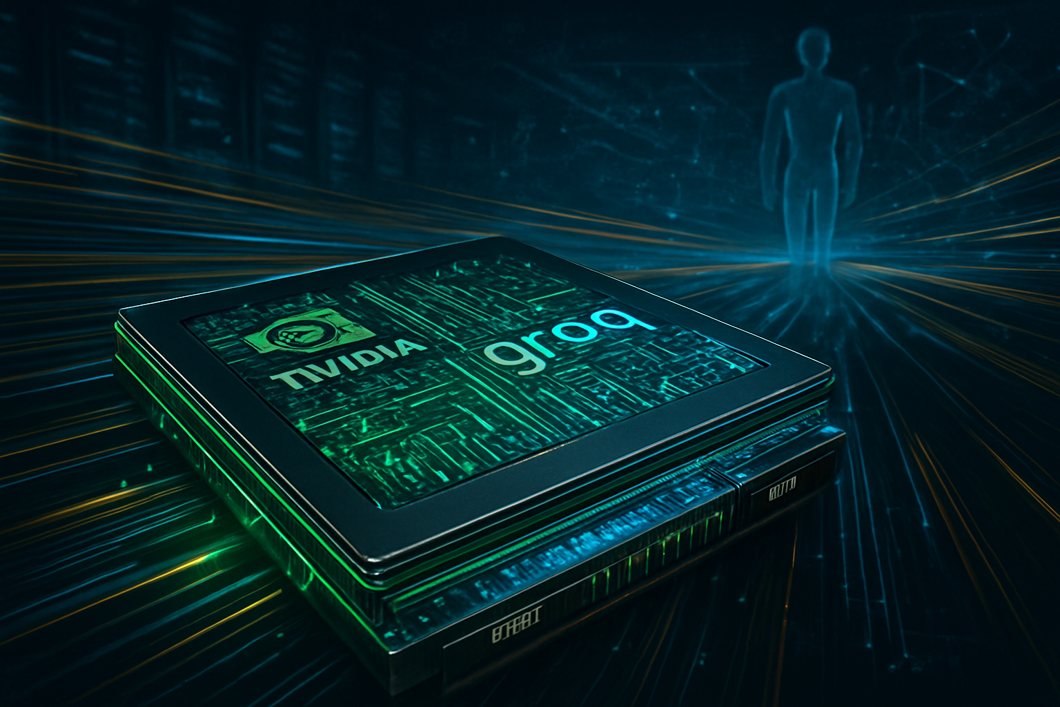
The Market Scramble: NVIDIA, AMD, and the Rise of Custom ASICs
The expansion of CoWoS capacity has profound implications for the competitive dynamics of the tech industry. NVIDIA remains the dominant force and the "anchor tenant" of TSMC’s packaging lines, reportedly securing over 60% of the total CoWoS capacity for 2025 and 2026. This preferential access has been a cornerstone of NVIDIA’s market lead, ensuring that as demand for its Blackwell and Rubin GPUs soared, it had the physical means to deliver them. For Advanced Micro Devices (NASDAQ: AMD), the expansion is equally vital. AMD’s Instinct MI350 and the upcoming MI400 series rely heavily on CoWoS-S and SoIC technologies to compete on memory bandwidth, and the increased supply from TSMC is the only way AMD can hope to gain market share in the enterprise AI space.
Beyond the traditional chipmakers, a new class of competitors is benefiting from TSMC’s scale. Cloud Service Providers (CSPs) like Alphabet (NASDAQ: GOOGL), Amazon (NASDAQ: AMZN), and Meta (NASDAQ: META) are increasingly designing their own custom AI Application-Specific Integrated Circuits (ASICs). These companies are now competing directly with NVIDIA and AMD for TSMC’s packaging slots. By securing direct capacity, these tech giants can optimize their data centers for specific internal workloads, potentially disrupting the standard GPU market. The strategic advantage has shifted: in 2026, the company that wins is the one with the most guaranteed "wafer-per-month" allocations at TSMC’s AP7 and AP8 facilities.
This massive capacity build-out also serves as a defensive moat for TSMC. While competitors like Intel (NASDAQ: INTC) and Samsung (KRX: 005930) are racing to develop their own advanced packaging solutions (such as Intel’s Foveros), TSMC’s sheer scale and proven yield rates for CoWoS-L have made it the nearly exclusive partner for high-end AI silicon. This concentration of power has solidified Taiwan’s role as the indispensable hub of the AI era, even as geopolitical concerns drive discussions about supply chain diversification.
Beyond Moore’s Law: The "More than Moore" Significance
The relentless expansion of CoWoS capacity is a clear signal that the semiconductor industry has entered the "More than Moore" era. For decades, progress was defined by shrinking transistors to fit more on a single chip. But as physical limits are reached and costs skyrocket, the industry has turned to "heterogeneous integration"—combining different types of chips (CPU, GPU, HBM) into a single, massive package. TSMC’s CoWoS is the physical manifestation of this trend, allowing for a level of performance that a single monolithic chip simply cannot achieve.
This shift has wider socio-economic implications. The massive capital expenditure required for these packaging plants—often exceeding $10 billion per site—means that only the largest players can survive. This creates a barrier to entry that may lead to further consolidation in the semiconductor industry. Furthermore, the environmental impact of these facilities, which require immense amounts of power and ultra-pure water, has become a central topic of discussion in Taiwan. TSMC has responded by committing to more sustainable manufacturing processes, but the sheer scale of the 2026 capacity targets makes this a monumental challenge.
Comparatively, this milestone is being viewed by historians as significant as the transition to EUV (Extreme Ultraviolet) lithography was a few years ago. Just as EUV was necessary to reach the 7nm and 5nm nodes, advanced packaging is now the "enabling technology" for the next decade of AI. Without it, the large language models (LLMs) and autonomous systems of the future would remain theoretical, trapped by the bandwidth limitations of traditional chip designs.
The Next Frontier: Panel-Level Packaging and Glass Substrates
Looking toward the latter half of 2026 and into 2027, the industry is already eyeing the next evolution: Fan-Out Panel-Level Packaging (FOPLP). While current CoWoS processes use round 12-inch wafers, FOPLP utilizes large rectangular panels. This transition, which TSMC is currently piloting at its Chiayi site, offers a significant leap in efficiency. Rectangular panels can fit more chips with less waste at the edges, potentially increasing the area utilization from 57% to over 80%. This will be essential as AI chips continue to grow in size, eventually reaching the point where even a 12-inch wafer is too small to be an efficient carrier.
Another major development on the horizon is the adoption of glass substrates. Unlike the organic materials used today, glass offers superior flatness and thermal stability, which are critical for the ultra-fine circuitry required in future 2nm and 1.6nm AI processors. Experts predict that the first commercial applications of glass-based advanced packaging will appear by late 2027, further extending the performance gains of the CoWoS lineage. The challenge remains the extreme fragility of glass during the manufacturing process, a hurdle that TSMC’s R&D teams are working to solve as they finalize the 2026 expansion.
Conclusion: A New Foundation for the AI Century
TSMC’s aggressive expansion of CoWoS capacity through 2026 marks the end of the "packaging bottleneck" era and the beginning of a new phase of AI scaling. By doubling its output and mastering complex technologies like CoWoS-L and SoIC, TSMC has provided the physical foundation upon which the next generation of artificial intelligence will be built. The transition from 35,000 to over 110,000 wafers per month is not just a logistical achievement; it is a fundamental reconfiguration of how high-performance computers are designed and manufactured.
As we move through 2026, the industry will be watching closely to see if TSMC can maintain its yield rates as it scales and whether competitors can finally mount a credible challenge to its packaging dominance. For now, the "Packaging War" has a clear leader. The long-term impact of this expansion will be felt in every sector touched by AI—from healthcare and autonomous transit to the very way we interact with technology. The bottleneck has been broken, and the race to fill that new capacity with even more powerful AI models has only just begun.
This content is intended for informational purposes only and represents analysis of current AI developments.
TokenRing AI delivers enterprise-grade solutions for multi-agent AI workflow orchestration, AI-powered development tools, and seamless remote collaboration platforms.
For more information, visit https://www.tokenring.ai/.