In a move that underscores the high-stakes complexity of the global semiconductor landscape, NVIDIA (NASDAQ: NVDA) has finalized a landmark $5 billion equity investment in Intel Corporation (NASDAQ: INTC), effectively becoming one of the company’s largest shareholders. The deal, which received Federal Trade Commission (FTC) approval in December 2025, positions the two longtime rivals as reluctant but deeply intertwined partners. However, the financial alliance comes with a stark technical caveat: despite the massive capital injection, NVIDIA has officially halted plans for mass production on Intel’s flagship 18A (1.8nm) process node, choosing instead to remain tethered to its primary manufacturing partner in Taiwan.
This "frenemy" dynamic highlights a strategic divergence between financial stability and technical readiness. While NVIDIA is willing to spend billions to ensure Intel remains a viable domestic alternative to the Taiwan Semiconductor Manufacturing Company (NYSE: TSM), it is not yet willing to gamble its market-leading AI hardware on Intel’s nascent manufacturing yields. For Intel, the investment provides a critical lifeline and a vote of confidence from the world’s most valuable chipmaker, even as it struggles to prove that its "five nodes in four years" roadmap can meet the exacting standards of the AI era.
Technical Roadblocks and the 18A Reality Check
Intel’s 18A process was designed to be the "Great Equalizer," the node that would finally allow the American giant to leapfrog TSMC in transistor density and power efficiency. By late 2025, Intel successfully moved 18A into High-Volume Manufacturing (HVM) for its internal products, including the "Panther Lake" client CPUs and "Clearwater Forest" server chips. However, the transition for external foundry customers has been far more turbulent. Reports from December 2025 indicate that NVIDIA’s internal testing of the 18A node yielded "disappointing" results, particularly regarding performance-per-watt metrics and wafer yields.
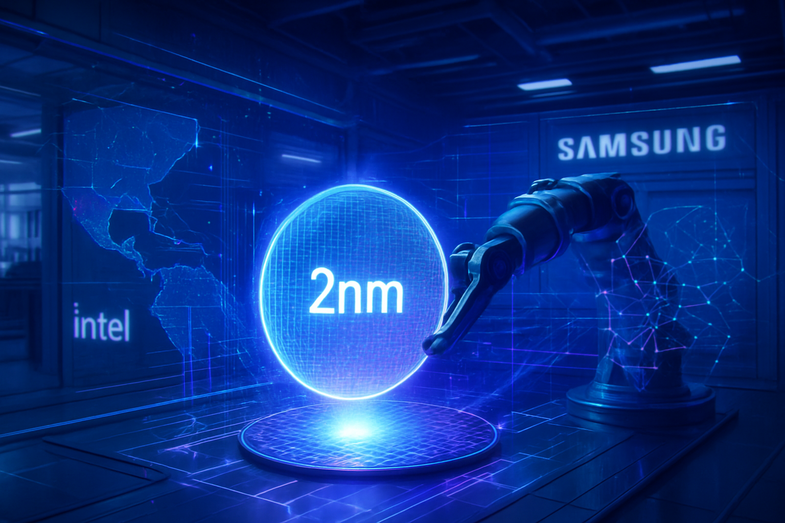
Industry insiders suggest that while Intel has improved 18A yields from a dismal 10% in early 2025 to roughly 55–65% by the fourth quarter, these figures still fall short of the 70–80% "gold standard" required for high-margin AI GPUs. For a company like NVIDIA, which commands nearly 90% of the AI accelerator market, even a minor yield deficit translates into billions of dollars in lost revenue. Consequently, NVIDIA has opted to keep its next-generation Blackwell successor on TSMC’s N2 (2nm) node, viewing Intel’s 18A as a bridge too far for current-generation mass production. This sentiment is reportedly shared by other industry titans like Broadcom (NASDAQ: AVGO) and AMD (NASDAQ: AMD), both of whom have conducted 18A trials but declined to commit to large-scale orders for 2026.
A Strategic Pivot: Co-Design and the AI PC Frontier
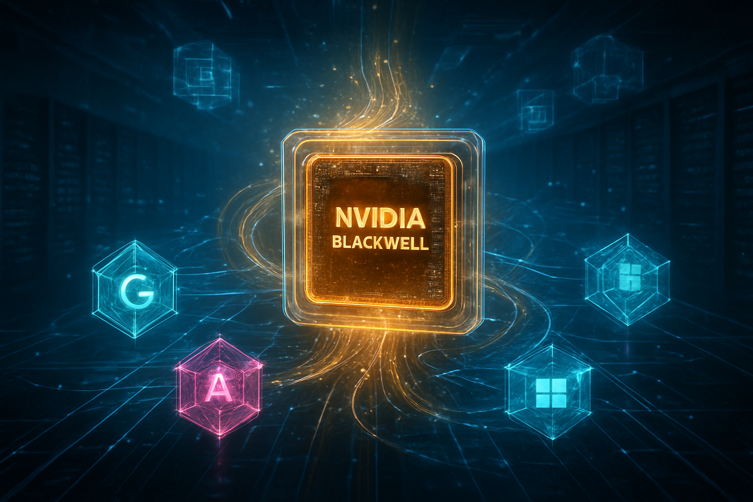
While the manufacturing side of the relationship is on hold, the $5 billion investment has opened the door to a new era of product collaboration. The deal includes a comprehensive agreement to co-design custom x86 data center CPUs specifically optimized for NVIDIA’s AI infrastructure. This move allows NVIDIA to move beyond its ARM-based Grace CPUs and offer a more integrated solution for legacy data centers that remain heavily invested in the x86 ecosystem. Furthermore, the two companies are reportedly working on a revolutionary System-on-Chip (SoC) for "AI PCs" that combines Intel’s high-efficiency CPU cores with NVIDIA’s RTX graphics architecture—a direct challenge to Apple’s M-series dominance.
This partnership serves a dual purpose: it bolsters Intel’s product relevance while giving NVIDIA a deeper foothold in the client computing space. For the broader tech industry, this signals a shift away from pure competition toward "co-opetition." By integrating their respective strengths, Intel and NVIDIA are creating a formidable front against the rise of ARM-based competitors and internal silicon efforts from cloud giants like Amazon and Google. However, the competitive implications for TSMC are mixed; while TSMC retains the high-volume manufacturing of NVIDIA’s most advanced chips, it now faces a competitor in Intel that is backed by the financial might of its own largest customers.
Geopolitics and the "National Champion" Hedge
The primary driver behind NVIDIA’s $5 billion investment is not immediate technical gain, but long-term geopolitical insurance. With over 90% of the world's most advanced logic chips currently produced in Taiwan, the semiconductor supply chain remains dangerously exposed to regional instability. NVIDIA CEO Jensen Huang has been vocal about the need for a "resilient, geographically diverse supply base." By taking a 4% stake in Intel, NVIDIA is essentially paying for a "Plan B." If production in the Taiwan Strait were ever disrupted, NVIDIA now has a vested interest—and a seat at the table—to ensure Intel’s Arizona and Ohio fabs are ready to pick up the slack.
This alignment has effectively transformed Intel into a "National Strategic Asset," supported by both the U.S. government through the CHIPS Act and private industry through NVIDIA’s capital. This "too big to fail" status ensures that Intel will have the necessary resources to continue its pursuit of process parity, even if it misses the mark with 18A. The investment acts as a bridge to Intel’s future 14A (1.4nm) node, which will utilize the world’s first High-NA EUV lithography machines. For NVIDIA, the $5 billion is a small price to pay to ensure that a viable domestic foundry exists by 2027 or 2028, reducing its existential dependence on a single geographic point of failure.
Looking Ahead: The Road to 14A and High-NA EUV
The focus of the Intel-NVIDIA relationship is now shifting toward the 2026–2027 horizon. Experts predict that the real test of Intel’s foundry ambitions will be the 14A node. Unlike 18A, which was seen by many as a transitional technology, 14A is being built from the ground up for the era of High-NA (Numerical Aperture) EUV. This technology is expected to provide the precision necessary to compete directly with TSMC’s most advanced future nodes. Intel has already taken delivery of the first High-NA machines from ASML, giving it a potential head start in learning the complexities of the next generation of lithography.
In the near term, the industry will be watching for the first samples of the co-designed Intel-NVIDIA AI PC chips, expected to debut in late 2026. These products will serve as a litmus test for how well the two companies can integrate their disparate engineering cultures. The challenge remains for Intel to prove it can function as a true service-oriented foundry, treating external customers with the same priority as its own internal product groups—a cultural shift that has proven difficult in the past. If Intel can successfully execute on 14A and provide the yields NVIDIA requires, the $5 billion investment may go down in history as one of the most prescient strategic moves in the history of the semiconductor industry.
Summary: A Fragile but Necessary Alliance
The current state of the Intel-NVIDIA relationship is a masterclass in strategic hedging. NVIDIA has successfully secured its future by investing in a domestic manufacturing alternative while simultaneously protecting its present by sticking with the proven reliability of TSMC. Intel, meanwhile, has gained a powerful ally and the capital necessary to weather its current yield struggles, though it remains under immense pressure to deliver on its technical promises.
As we move into 2026, the key metrics to watch will be Intel’s 14A development milestones and the market reception of the first joint Intel-NVIDIA hardware. This development marks a significant chapter in AI history, where the physical constraints of geography and manufacturing have forced even the fiercest of rivals into a symbiotic embrace. For now, NVIDIA is betting on Intel’s survival, even if it isn't yet ready to bet on its 18A silicon.
This content is intended for informational purposes only and represents analysis of current AI developments.
TokenRing AI delivers enterprise-grade solutions for multi-agent AI workflow orchestration, AI-powered development tools, and seamless remote collaboration platforms.
For more information, visit https://www.tokenring.ai/.