The abrupt departure of Pat Gelsinger as CEO of Intel Corporation (NASDAQ: INTC) in December 2024 sent shockwaves through the global technology sector, marking the end of a high-stakes gamble to restore the American chipmaker to its former glory. Gelsinger, a legendary engineer who returned to Intel in 2021 with a "Saviour" mandate, was reportedly forced to resign after a tense board meeting where directors, led by independent chair Frank Yeary, confronted him with a $16.6 billion net loss and a stock price that had cratered by over 60% during his tenure. His exit signaled the definitive failure of the initial phase of his "IDM 2.0" strategy, which sought to simultaneously design world-class chips and build a massive foundry business to rival TSMC.
As of late 2025, the dust has finally settled on the most tumultuous leadership transition in Intel’s 57-year history. Under the disciplined hand of new CEO Lip-Bu Tan—the former Cadence Design Systems (NASDAQ: CDNS) chief who took the helm in March 2025—Intel has pivoted from Gelsinger’s "grand vision" to a "back-to-basics" execution model. This shift has not only stabilized the company's financials but has also led to an unprecedented 10% equity stake from the U.S. government, effectively transforming Intel into a "National Champion" and a critical instrument of American industrial policy.
Technical Execution: The 18A Turning Point
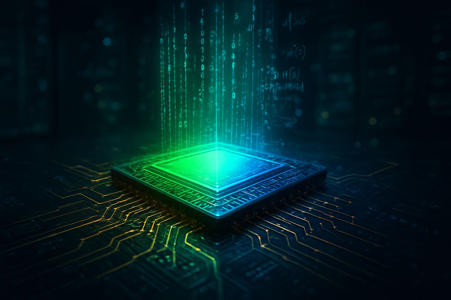
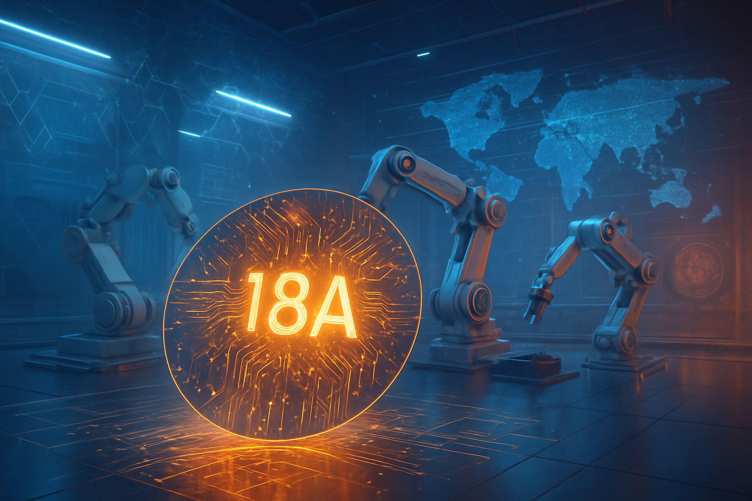
The core of Intel’s survival hinges on the technical success of its 18A (1.8nm) manufacturing process. As of December 2025, Intel has officially entered High-Volume Manufacturing (HVM) for 18A, successfully navigating a "valley of death" where early yield reports were rumored to be as low as 10%. Under Lip-Bu Tan’s leadership, engineering teams focused on stabilizing the node’s two most revolutionary features: RibbonFET (Gate-All-Around transistors) and PowerVia (Backside Power Delivery). By late 2025, yields have reportedly climbed to the 60% range—still trailing the 75% benchmarks of Taiwan Semiconductor Manufacturing Co. (NYSE: TSM), but sufficient to power Intel’s latest Panther Lake and Clearwater Forest processors.
The technical significance of 18A cannot be overstated; it represents the first time in a decade that Intel has achieved a performance-per-watt lead over its rivals in specific AI and server benchmarks. By implementing Backside Power Delivery ahead of TSMC—which is not expected to fully deploy the technology until 2026—Intel has created a specialized advantage for high-performance computing (HPC) and AI accelerators. This technical "win" has been the primary catalyst for the company’s stock recovery, which has surged from a 2024 low of $17.67 to nearly $38.00 in late 2025.
A New Competitive Order: The Foundry Subsidiary Model
The post-Gelsinger era has brought a radical restructuring of Intel’s business model. To address the inherent conflict of interest in being both a chip designer and a manufacturer for rivals, Intel Foundry was spun off into a wholly-owned independent subsidiary in early 2025. This move was designed to provide the "firewall" necessary to attract major customers like NVIDIA (NASDAQ: NVDA) and Apple (NASDAQ: AAPL). While Intel still manufactures the vast majority of its own chips, the foundry has secured "anchor" customers in Microsoft (NASDAQ: MSFT) and Amazon (NASDAQ: AMZN), both of whom are now fabbing custom AI silicon on the 18A node.
This restructuring has shifted the competitive landscape from a zero-sum game to one of "managed competition." While Advanced Micro Devices (NASDAQ: AMD) remains Intel’s primary rival in the CPU market, the two companies have entered preliminary discussions regarding specialized server "tiles" manufactured in Intel’s Arizona fabs. This "co-opetition" model reflects a broader industry trend where the sheer cost of leading-edge manufacturing—now exceeding $20 billion per fab—requires even the fiercest rivals to share infrastructure to maintain the pace of the AI revolution.
The Geopolitics of the 'National Champion'
The most significant development of 2025 is the U.S. government’s decision to take a 9.9% equity stake in Intel. This $8.9 billion intervention, finalized in August 2025, has fundamentally altered Intel’s identity. No longer just a private corporation, Intel is now the "National Champion" of the U.S. semiconductor industry. This status comes with a $3.2 billion "Secure Enclave" contract, making Intel the exclusive provider of advanced chips for the U.S. military, and grants Washington a de facto veto over any major strategic shifts or potential foreign acquisitions.
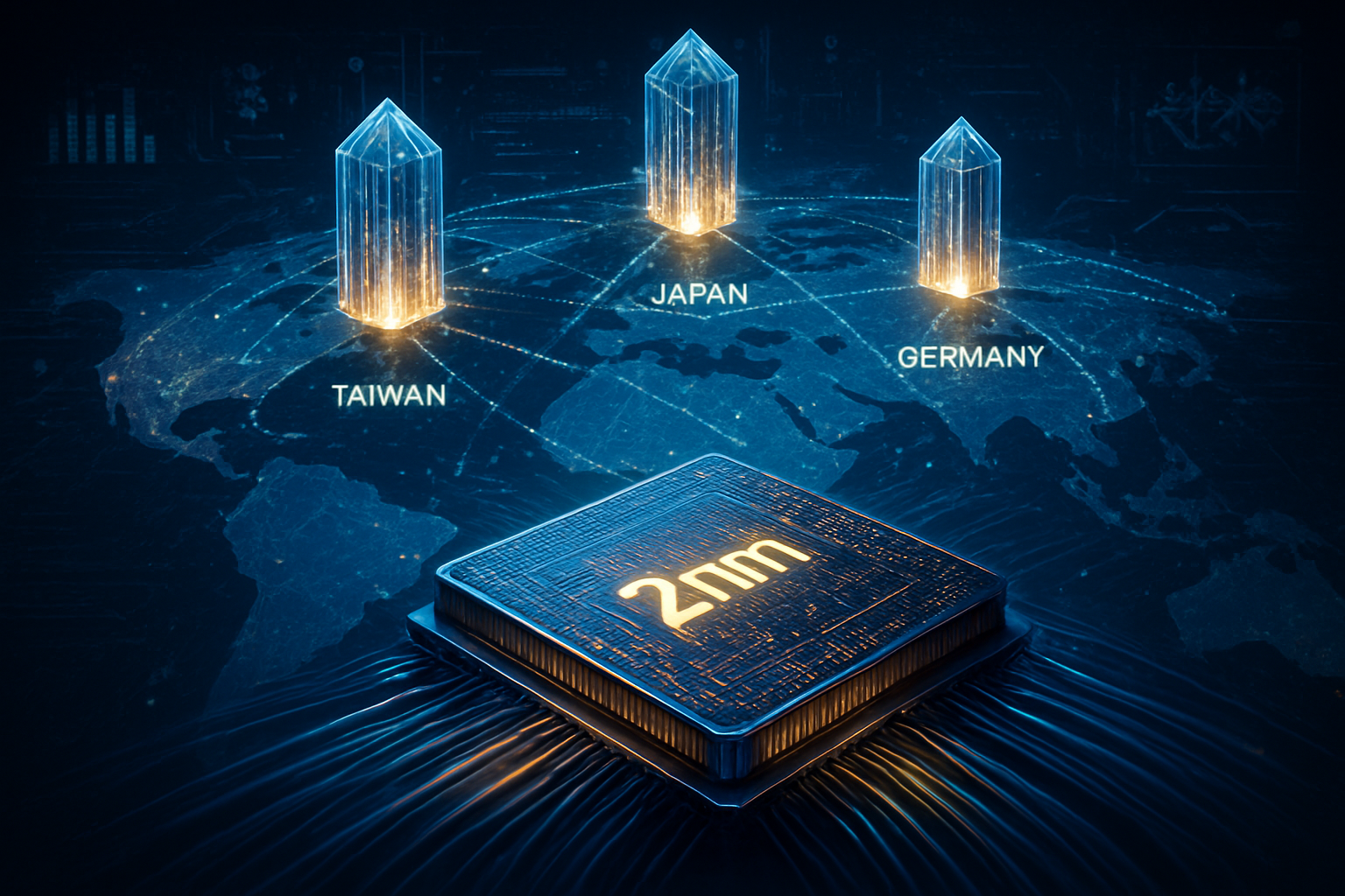
This "state-backed" model has created a new set of geopolitical challenges. Relations with China have soured further, with Beijing imposing retaliatory tariffs as high as 125% on Intel products and raising concerns about "backdoors" in government-linked hardware. Consequently, Intel’s revenue from the Chinese market—once nearly 30% of its total—has begun a slow, painful decline. Meanwhile, the U.S. stake is explicitly intended to reduce global reliance on Taiwan, creating a delicate diplomatic dance with TSMC as the U.S. attempts to build a domestic "moat" without alienating its most important technological partner in the Pacific.
The Road Ahead: 2026 and Beyond
Looking toward 2026, Intel faces a "show-me" period where it must prove that its 18A yields can match the profitability of TSMC’s mature nodes. The immediate focus for CEO Lip-Bu Tan is the rollout of the 14A (1.4nm) node, which will utilize the world’s first "High-NA" EUV (Extreme Ultraviolet) lithography machines in a production environment. Success here would solidify Intel’s technical parity, but the financial burden remains immense. Despite a 15% workforce reduction and the cancellation of multi-billion dollar projects in Germany and Poland, Intel’s free cash flow remains under significant pressure.
Experts predict that the next 12 to 18 months will see a consolidation of the "National Champion" strategy. This may include further government-led "forced synergies," such as a potential joint venture between Intel and TSMC’s U.S.-based operations to share the massive overhead of American manufacturing. The challenge will be maintaining the agility of a tech giant while operating under the heavy regulatory and political oversight that comes with being a state-backed enterprise.
Conclusion: A Fragile Resurrection
Pat Gelsinger’s departure was the painful but necessary catalyst for Intel’s transformation. While his "IDM 2.0" vision provided the blueprint, it required a different kind of leader—one focused on fiscal discipline rather than charismatic projections—to make it a reality. By late 2025, Intel has successfully "stopped the bleeding," leveraging the 18A node and a historic U.S. government partnership to reclaim its position as a viable alternative to the Asian foundry monopoly.
The significance of this development in AI history is profound: it marks the moment the U.S. decided it could no longer leave the manufacturing of the "brains" of AI to the free market alone. As Intel enters 2026, the world will be watching to see if this "National Champion" can truly innovate at the speed of its private-sector rivals, or if it will become a subsidized relic of a bygone era. For now, the "Intel Inside" sticker represents more than just a CPU; it represents the front line of a global struggle for technological sovereignty.
This content is intended for informational purposes only and represents analysis of current AI developments.
TokenRing AI delivers enterprise-grade solutions for multi-agent AI workflow orchestration, AI-powered development tools, and seamless remote collaboration platforms.
For more information, visit https://www.tokenring.ai/.