Tag: AI Hardware

  • The Great Decoupling: How RISC-V Achieved Architecture Sovereignty in 2026

    The Great Decoupling: How RISC-V Achieved Architecture Sovereignty in 2026

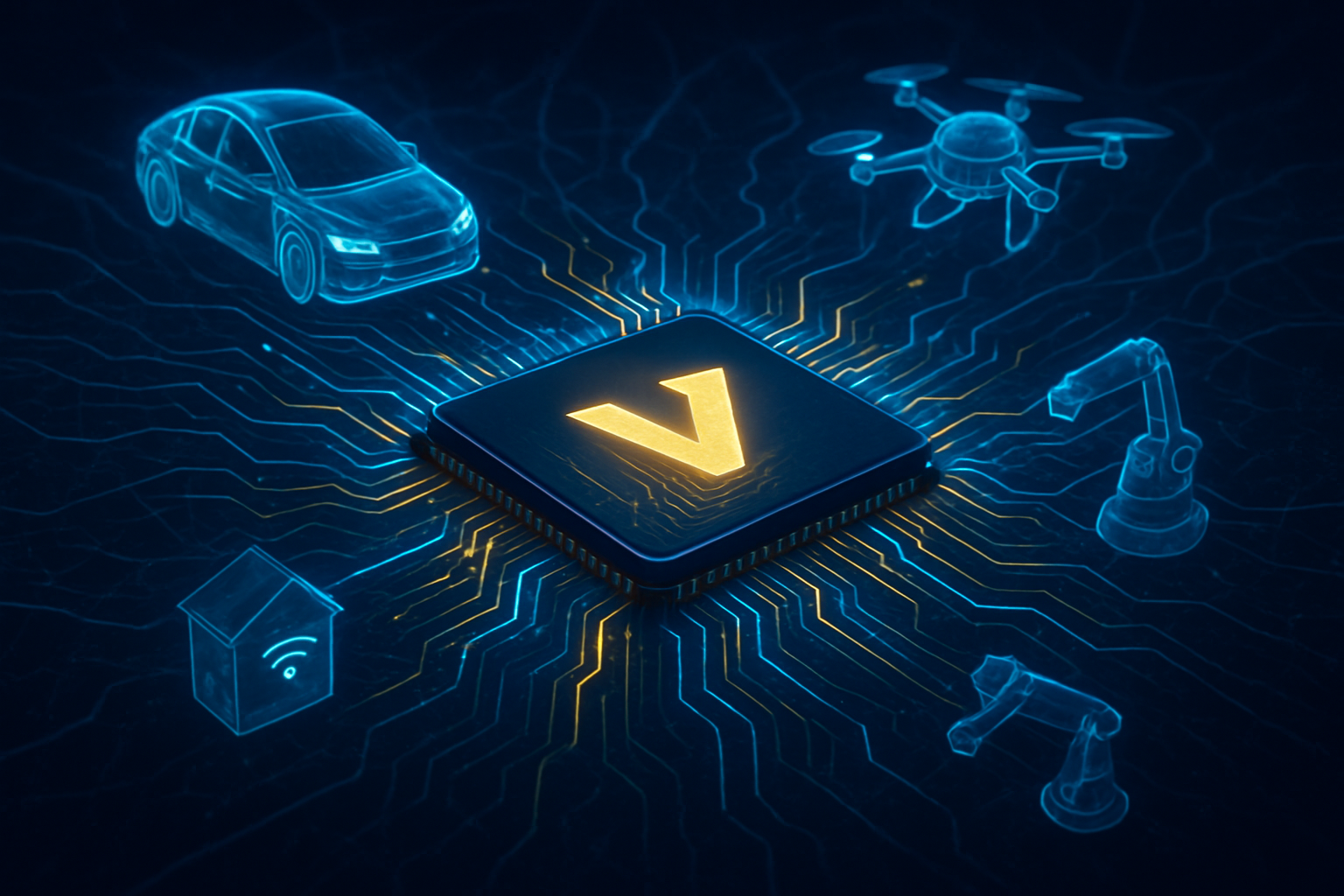
    As of February 2026, the global semiconductor landscape has undergone a tectonic shift, marking the end of the long-standing x86 and ARM duopoly. RISC-V, the open-standard Instruction Set Architecture (ISA), has matured from a promising academic project into a dominant industrial powerhouse. This evolution is most visible in the automotive and Internet of Things (IoT) sectors, where the architecture now commands a staggering 25% and 55% of new design wins respectively. By offering a royalty-free, highly customizable alternative, RISC-V has become the cornerstone of the "Software-Defined Everything" era, enabling a new level of hardware-software co-design that was previously impossible under restrictive proprietary licenses.

    The significance of this milestone cannot be overstated. For decades, chip designers were forced to choose between the high-performance but power-hungry x86 architecture or the efficient but strictly controlled ARM ecosystem. Today, RISC-V provides a third pillar that balances performance with unprecedented flexibility. This "architecture sovereignty" allows tech giants and startups alike to bake their own proprietary AI accelerators and safety features directly into the processor core. As the industry moves toward 2027, the "ARM Tax"—the multi-million dollar licensing fees and per-chip royalties—has shifted from a standard business expense to a competitive liability, driving a massive migration toward the open-source frontier.

    Technical Maturity: From Embedded Controllers to High-Performance AI

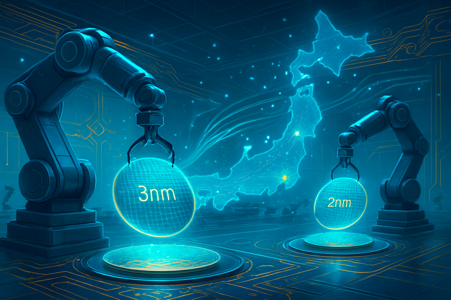
    The technical breakthrough that defined 2025 and 2026 was the finalization and widespread implementation of the RVA23 profile. Previously, RISC-V faced criticism for "fragmentation," where different chip makers implemented features in incompatible ways. The RVA23 standard unified the ecosystem, providing a stable baseline for operating systems like Android and enterprise Linux distributions. In April 2026, the release of Ubuntu 26.04 LTS became a landmark event, offering the first long-term supported enterprise OS with native, high-performance optimization for RISC-V, effectively putting it on equal footing with x86 for server and edge applications.

    A key technical differentiator in 2026 is the RISC-V Vector (RVV) 1.0 extension. Unlike ARM (Nasdaq: ARM) or Intel (Nasdaq: INTC) architectures, which often require separate, specialized AI chips, RISC-V’s vector extensions allow for massive parallel processing of AI workloads directly within the CPU. Companies like Tenstorrent and SiFive have released "Ascalon-class" cores that rival the performance of ARM’s Neoverse V3. These chips use 512-bit vector widths to handle complex sensor fusion and machine learning telemetry in real-time, which has proven critical for the low-latency requirements of autonomous systems.

    Furthermore, the rise of "Shift-Left" development methodologies has been accelerated by RISC-V’s open nature. Automakers are now using "Digital Twins" of RISC-V hardware—fully functional software models of the chip—to begin writing and testing vehicle code years before a physical chip is even manufactured. This has reduced the development cycle for new vehicle platforms from the traditional five years down to just three. Because the ISA is open, developers can inspect every instruction, ensuring that safety-critical "Zero Trust" security protocols are hard-coded into the silicon, a level of transparency that proprietary architectures cannot match.

    The software ecosystem has finally caught up to the hardware. In late 2025, Google (Nasdaq: GOOGL) designated RISC-V as a "Tier 1" architecture for Android, finalizing the Native Development Kit (NDK) and Application Binary Interface (ABI). This move has paved the way for the first wave of commercial RISC-V smartphones appearing in early 2026. While these devices currently target the mid-range and budget markets in Asia, the technical foundation is now in place for RISC-V to challenge ARM’s 95% dominance of the mobile processor market by the end of the decade.

    The Economic Earthquake: Challenging the ARM and x86 Giants

    The maturation of RISC-V has sent shockwaves through the boardrooms of established chip giants. Qualcomm (Nasdaq: QCOM), once one of ARM’s largest customers, has aggressively pivoted toward RISC-V following high-profile licensing disputes. By acquiring Ventana Micro Systems in 2025, Qualcomm has begun integrating its own high-performance RISC-V cores into its Snapdragon automotive and IoT platforms. This strategic move allows Qualcomm to bypass ARM’s restrictive licensing terms and potentially save billions in royalty payments over the next decade, while gaining the freedom to innovate at the instruction level.

    In the automotive sector, the Quintauris joint venture—a powerhouse consortium including Bosch, Infineon (OTC: IFNNY), Nordic Semiconductor, NXP (Nasdaq: NXPI), and Qualcomm—has successfully established a standardized RISC-V platform for Software-Defined Vehicles (SDVs). By early 2026, this venture has turned RISC-V into the industry standard for zonal controllers, the "brains" that manage everything from power steering to infotainment. This collective approach has effectively neutralized ARM’s historical advantage in the automotive space, as manufacturers now prefer a communal, open-source architecture that no single company can gatekeep or monopolize.

    The impact on the IoT market has been even more dramatic. With over 55% of new IoT designs now utilizing RISC-V, the architecture has become the default choice for connected devices. The royalty-free model has reduced bill-of-materials (BOM) costs by as much as 50% for high-volume sensors and smart home devices. This cost advantage has allowed companies to reinvest savings into more robust on-device AI and security features. For startups, the low barrier to entry provided by RISC-V has sparked a renaissance in "bespoke silicon," where small teams can design custom chips for niche industrial applications without the $10 million+ upfront licensing costs associated with proprietary ISAs.

    Legacy players are reacting with varying degrees of urgency. While Intel has embraced RISC-V through its foundry services (IFS), offering to manufacture RISC-V chips for others, it faces a long-term threat to its x86 dominance in the data center. Meta (Nasdaq: META) and NVIDIA (Nasdaq: NVDA) have already integrated millions of RISC-V cores into their internal infrastructure—Meta for its MTIA AI inference accelerators and NVIDIA for managing telemetry and secure boot across its entire GPU lineup. For these giants, RISC-V isn't just a cost-saving measure; it’s a strategic tool for vertical integration, allowing them to control the entire stack from the silicon to the cloud.

    A New Era of Open-Source Infrastructure and Global Resilience

    The rise of RISC-V in 2026 represents a broader trend toward technological de-globalization and national self-reliance. As trade tensions continue to influence the tech sector, RISC-V has emerged as a "neutral" architecture. Because no single nation or company owns the ISA, it serves as a common language for global innovation that is immune to specific export bans or entity-list restrictions. This has made RISC-V particularly attractive in the European Union and Asia, where governments are subsidizing open-source hardware projects to ensure their domestic industries are not overly dependent on US- or UK-based IP.

    This shift mirrors the "Linux moment" for hardware. Just as Linux broke the monopoly of proprietary operating systems in the 1990s and 2000s, RISC-V is doing the same for the processor world. The architecture has fostered a massive, global community of contributors, ensuring that security vulnerabilities are patched faster and optimizations are shared more broadly than in closed ecosystems. The 2026 landscape shows that "Security through Transparency" has won over "Security through Obscurity," with many government agencies now mandating RISC-V for critical infrastructure to ensure there are no hidden backdoors in the silicon.

    However, this transition has not been without its challenges. The industry has had to grapple with the "Wild West" period of RISC-V development, where early adopters struggled with a lack of standardized tools and middleware. The successful stabilization of the ecosystem in 2026 is largely credited to the RISC-V International organization, which managed to herd the competing interests of hundreds of member companies toward a common goal. This level of industry cooperation is unprecedented and serves as a model for how other complex technologies, such as quantum computing and advanced robotics, might be governed in the future.

    Comparisons to previous AI milestones are frequent. Analysts often liken the maturity of RISC-V to the launch of ChatGPT—a moment where a technology that had been "bubbling under the surface" for years suddenly achieved the performance and accessibility needed to change the world overnight. While ChatGPT revolutionized how we interact with data, RISC-V is revolutionizing the physical substrate upon which that data is processed. It is the silent engine driving the AI revolution at the edge, making sophisticated intelligence affordable, customizable, and ubiquitous.

    The Horizon: AI-Native Silicon and the Path to the Data Center

    Looking ahead to 2027 and beyond, the focus of the RISC-V community is shifting toward the high-performance computing (HPC) and server markets. While RISC-V has conquered IoT and made significant inroads into automotive, the data center remains the "final frontier" currently dominated by x86 and ARM. Experts predict that the next two years will see the rise of "AI-Native" servers, where RISC-V’s modularity allows for the seamless integration of hundreds of specialized neural cores on a single die. This could potentially disrupt the server market by offering significantly higher performance-per-watt for the specific math required by Large Language Models (LLMs).

    We are also likely to see the emergence of the first true "Open-Source Consumer Ecosystem." With Android support finalized, the dream of a fully open-source laptop and smartphone—from the hardware instructions to the kernel to the user interface—is becoming a reality. This will likely appeal to a growing market of privacy-conscious consumers and enterprise users who require absolute control over their hardware. The challenge will be in hardware-software optimization; while RISC-V is capable, it will take time to match the decades of "fine-tuning" that Intel and Apple (Nasdaq: AAPL) have applied to their proprietary platforms.

    Predictions for 2028 suggest that RISC-V will reach 15% of the total CPU market share, a meteoric rise considering its near-zero presence a decade prior. To reach this goal, the ecosystem must address the remaining gaps in high-end developer tools and ensure a steady pipeline of talent. Universities worldwide have already shifted their computer architecture curricula to center on RISC-V, ensuring that the next generation of engineers is "native" to the open-source model. As the "great decoupling" from proprietary architectures continues, the momentum behind RISC-V appears not just sustainable, but inevitable.

    Summary of a New Computing Paradigm

    The state of RISC-V in early 2026 is one of undeniable maturity and massive momentum. What began as a research project at UC Berkeley has fundamentally reordered the $600 billion semiconductor industry. By dominating the IoT sector and becoming the standard for the next generation of Software-Defined Vehicles, RISC-V has proven that an open-source model can outpace and out-innovate even the most entrenched proprietary giants. The royalty-free nature of the ISA has democratized silicon design, sparking a wave of innovation that is bringing AI and advanced connectivity to every corner of the global economy.

    As we move through 2026, the industry should watch for the first commercial RISC-V mobile devices and the continued expansion of RISC-V into the data center. The "Architecture Wars" are far from over, but the battlefield has changed. No longer is the question whether RISC-V is viable; the question is how quickly the remaining proprietary strongholds will adapt to a world where the foundations of computing are free, open, and available to all. The "Great Decoupling" is here, and it is powered by RISC-V.


    This content is intended for informational purposes only and represents analysis of current AI and semiconductor developments as of February 2026.

    TokenRing AI delivers enterprise-grade solutions for multi-agent AI workflow orchestration, AI-powered development tools, and seamless remote collaboration platforms.
    For more information, visit https://www.tokenring.ai/.

  • The New Moore’s Law: How Chiplets and CoWoS are Redefining the Scaling Paradigm in the AI Era

    The New Moore’s Law: How Chiplets and CoWoS are Redefining the Scaling Paradigm in the AI Era

    The semiconductor industry has reached a historic inflection point. For five decades, the industry followed the traditional Moore’s Law, doubling transistor density by physically shrinking the components on a single piece of silicon. However, as of February 2026, that "geometrical scaling" has hit a physical and economic wall. In its place, a "New Moore’s Law"—more accurately described as System-level Moore’s Law—has emerged, shifting the focus from the individual chip to the entire package. This evolution is driven by the insatiable compute demands of generative AI, where performance is no longer defined by how many transistors can fit on a die, but by how many dies can be seamlessly stitched together in 3D space.

    The primary engines of this revolution are Chip-on-Wafer-on-Substrate (CoWoS) and vertical 3D stacking technologies. By abandoning the "monolithic" approach—where a processor is carved from a single piece of silicon—industry leaders are now building massive, multi-die systems that bypass the traditional limits of physics. This shift represents the most significant architectural change in computing history since the invention of the integrated circuit, effectively decoupling performance gains from the slow and increasingly expensive progress of lithography nodes.

    The Death of the Monolithic Die and the Rise of CoWoS-L

    The technical heart of this shift lies in overcoming the "reticle limit." For years, the maximum size of a single chip was restricted to approximately 858mm²—the physical size of the mask used in lithography. To build the massive processors required for 2026-era AI, such as the NVIDIA (NASDAQ: NVDA) Rubin R100, engineers have turned to Advanced Packaging. TSMC (NYSE: TSM) has pioneered CoWoS-L (Local Silicon Interconnect), which uses tiny silicon bridges to "stitch" multiple logic dies together on an organic substrate. This allows a single package to effectively behave as one massive processor, far exceeding the physical size limits of traditional manufacturing.

    Beyond mere size, the industry has moved into the realm of true 3D integration with System on Integrated Chips (SoIC). Unlike 2.5D packaging, where chips sit side-by-side, SoIC allows for "bumpless" hybrid bonding, stacking logic directly on top of logic or memory. This reduces the distance data must travel from millimeters to micrometers, slashing power consumption and nearly eliminating the latency that previously throttled AI performance. Initial reactions from the research community have been transformative; experts note that the interconnect density provided by SoIC is now a more critical metric for AI training speeds than the raw clock speed of the transistors themselves.

    Strategic Realignment: The System Foundry Model

    This transition has fundamentally altered the competitive landscape for tech giants and foundries. TSMC has maintained its dominance by aggressively expanding its advanced packaging capacity to over 140,000 wafers per month in early 2026. This "System Foundry" approach allows them to offer a full-stack solution: 2nm logic, 3D stacking, and CoWoS-L packaging. Meanwhile, Intel (NASDAQ: INTC) has pivoted its strategy to position its Advanced System Assembly and Test (ASAT) business as a standalone service. By offering Foveros Direct 3D and EMIB packaging to external customers, Intel is attempting to capture the growing market for custom AI ASICs from cloud providers like Amazon and Google.

    Advanced Micro Devices (NASDAQ: AMD) has also leveraged these developments to close the gap with market leaders. The newly released Instinct MI400 series utilizes SoIC-X technology to stack HBM4 memory directly onto the GPU logic, achieving a staggering 20 TB/s of memory bandwidth. This strategic move highlights the "Memory Wall" as the primary bottleneck in LLM training; by using vertical integration, AMD can provide memory capacities that were physically impossible under old monolithic designs. For startups and smaller AI labs, the emergence of chiplet "standardization" means they can now design custom accelerators using off-the-shelf high-performance chiplets, lowering the barrier to entry for specialized AI hardware.

    Solving the "Warpage Wall" and the Memory Bottleneck

    The wider significance of the "New Moore's Law" extends beyond performance; it is a response to the "Warpage Wall." As packages grow larger than 100mm per side to accommodate dozens of chiplets, traditional organic substrates tend to warp under the intense heat generated by 1,000-watt AI GPUs. This has led to the first commercial rollout of glass substrates in early 2026, led by Intel and Samsung (KOSPI: 005930). Glass provides superior thermal stability and flatness, enabling the ultra-fine interconnects required for next-generation 3D stacking.

    Furthermore, this era marks the beginning of the "System Technology Co-Optimization" (STCO) phase. Previously, chip design and packaging were separate steps; now, they are unified. This fits into the broader AI landscape by addressing the catastrophic power consumption of modern data centers. By integrating Silicon Photonics and Co-Packaged Optics (CPO) directly into the package, companies can now convert electrical signals to light within the processor itself. This bypasses the energy-intensive process of pushing electrons through copper cables, a milestone that compares in significance to the transition from vacuum tubes to transistors.

    The Road to the Trillion-Transistor Package

    Looking ahead, the industry is aligned on a singular goal: the trillion-transistor package by 2030. In the near term, we expect to see the "Base Die" revolution, where the bottom layer of a 3D stack handles all power delivery and routing, leaving the top layers dedicated purely to computation. This will likely lead to "liquid-to-chip" cooling becoming a standard requirement for high-end AI clusters, as the heat density of 3D-stacked chips begins to exceed the limits of traditional air and even current water-cooling methods.

    However, challenges remain. The complexity of testing 3D-stacked chips is immense—if one "chiplet" in a stack of ten is faulty, the entire expensive package may be lost. Experts predict that "Self-Healing Silicon," which can reroute circuits around manufacturing defects in real-time, will be the next major area of research. Additionally, the geopolitical concentration of advanced packaging capacity in Taiwan remains a point of concern for global supply chain resilience, prompting a frantic race to build similar facilities in the United States and Europe.

    A New Architecture for a New Era

    The evolution of chiplets and CoWoS represents more than just a clever engineering workaround; it is a fundamental shift in how humanity builds thinking machines. The "New Moore’s Law" acknowledges that while we can no longer make transistors significantly smaller, we can make the systems they inhabit significantly more complex and efficient. The transition from 2D to 3D, and from copper to light, ensures that the AI revolution will not be throttled by the physical limits of a single silicon wafer.

    As we move through 2026, the primary metric of progress will be "transistors per package." With the arrival of glass substrates, HBM4, and 3D SoIC, the roadmap for AI hardware has been extended by another decade. The coming months will be defined by the "Packaging Wars," as foundries and chip designers race to secure the capacity needed to build the world’s most powerful systems. The monolithic era is over; the era of the integrated system has begun.


    This content is intended for informational purposes only and represents analysis of current AI developments.

    TokenRing AI delivers enterprise-grade solutions for multi-agent AI workflow orchestration, AI-powered development tools, and seamless remote collaboration platforms.
    For more information, visit https://www.tokenring.ai/.

  • India’s Silicon Sovereignty: The 2026 Emergence of a Global Semiconductor Powerhouse

    India’s Silicon Sovereignty: The 2026 Emergence of a Global Semiconductor Powerhouse

    As of February 6, 2026, the global technology landscape has undergone a tectonic shift. India, once viewed as merely a software services giant, has successfully pivoted to become a cornerstone of the world’s hardware supply chain. The "Made in India" chip is no longer a strategic ambition but a commercial reality, with major manufacturing facilities officially coming online this month. This transformation is anchored by the aggressive $18 billion India Semiconductor Mission (ISM), which has successfully leveraged government incentives to attract over $90 billion in cumulative private investment.

    The immediate significance of this development cannot be overstated. By establishing a robust presence in both front-end wafer fabrication and back-end assembly, India has provided the global tech industry with a much-needed "China Plus One" alternative. With the recent commencement of full-scale commercial production at Micron Technology, Inc. (NASDAQ: MU) in Sanand, Gujarat, India has entered the elite league of nations capable of high-volume semiconductor manufacturing, fundamentally altering the risk profile of the global electronics trade.

    From Groundbreaking to Grid-Scale Production: The Technical Milestone

    The technical cornerstone of India’s 2026 semiconductor success is the transition from pilot testing to mass-market output. Micron Technology’s $2.75 billion facility in Sanand is now operating at peak capacity, churning out high-density DRAM and NAND flash memory chips. These components are being integrated into everything from mobile devices to data center servers, marking the first time Indian-produced memory has hit the international market at scale. Micron has already invited bids for Phase 2 of its Sanand campus, aiming to double its cleanroom space to meet the surging global demand for AI-optimized storage.

    Simultaneously, the Tata Group, through its subsidiary Tata Electronics, has reached a critical "tool-in" phase at its $11 billion mega-fab in Dholera. This facility, built in partnership with Taiwan’s Powerchip Semiconductor Manufacturing Corp (TWSE: 6770), is currently installing specialized lithography equipment to produce 28nm and 55nm logic chips. While 28nm is considered a mature node, it remains the workhorse for automotive, IoT, and power management applications—sectors where India is quickly becoming a primary supplier. The first commercial rollout of these 28nm chips is slated for late 2026, representing a massive leap in domestic technical capability.

    Further east, in Jagiroad, Assam, the Tata OSAT (Outsourced Semiconductor Assembly and Test) facility is nearing its April 2026 commissioning date. With a staggering projected capacity of 48 million chips per day, this facility specializes in advanced packaging techniques like Flip Chip and Integrated Systems Packaging (ISP). This high-volume back-end capacity is crucial for the global AI industry, which relies on sophisticated packaging to boost the performance of AI accelerators and edge computing hardware.

    Corporate Realignments and the Competitive Landscape

    The emergence of India as a hub has sent ripples through the corporate world, benefiting both local conglomerates and international tech giants. CG Power and Industrial Solutions Ltd. (NSE: CGPOWER), in a joint venture with Renesas Electronics Corporation (TSE: 6723) and Stars Microelectronics, has entered the pilot production phase for specialized power and analog chips. This partnership is strategically positioned to serve the global electric vehicle (EV) market, where Renesas is a dominant player, providing them with a resilient manufacturing base outside of East Asia.

    For tech giants like Apple Inc. (NASDAQ: AAPL) and Cisco Systems, Inc. (NASDAQ: CSCO), the Indian semiconductor ecosystem offers a double-edged advantage: supply chain diversification and reduced trade costs. Recent adjustments in US-India trade policies have seen import tariffs on Indian-made electronics drop to 18%, significantly lower than the 34%+ often levied on Chinese components. This has led Apple to integrate Indian-packaged memory and power management chips into its latest product lines, effectively de-risking its hardware stack from single-region geopolitical tensions.

    The competitive pressure is also being felt by traditional semiconductor hubs. As India scales, it is drawing significant Foreign Direct Investment (FDI) that might previously have gone to Vietnam or Southeast Asia. Startups in the Indian ecosystem are also benefiting; firms like Kaynes Semi and Logic Fruit Technologies are now designing indigenous AI accelerators and edge-compute platforms, leveraging the proximity of local manufacturing to iterate faster than ever before.

    AI Integration and Global Supply Chain Resilience

    India’s semiconductor rise is inextricably linked to the global AI revolution. The government has strategically aligned the India Semiconductor Mission with the national "IndiaAI" initiative, deploying over 34,000 GPUs across the country to create a "Compute-as-a-Public-Good" infrastructure. The chips being produced and packaged in India are increasingly tailored for these AI workloads. For instance, Tower Semiconductor (NASDAQ: TSEM) has recently entered a high-profile collaboration with NVIDIA Corporation (NASDAQ: NVDA) to produce silicon photonics components in India—technology that is essential for high-speed data transfer in AI data centers.

    This development addresses one of the most pressing concerns of the decade: the "single-region risk" associated with Taiwan and China. By 2026, India has established itself as a "trusted geography," a status that is attracting Western defense and aerospace contractors who require secure, transparent supply chains. The success of the ISM has also spurred the development of a domestic "full-stack" ecosystem, including local manufacturing of semiconductor chemicals and high-purity gases, which were previously imported.

    However, the rapid growth has not been without its challenges. Concerns regarding water intensity and the high energy requirements of wafer fabs have forced the Indian government to invest heavily in green energy corridors specifically for semiconductor parks. Furthermore, while India has succeeded in mature nodes, the race for leading-edge (sub-7nm) manufacturing remains a hurdle that the country is only beginning to address through research partnerships with international labs.

    The Horizon: ISM 2.0 and Beyond

    Looking ahead, the Indian government has already pivoted to "ISM 2.0," a second phase of the mission announced in the February 2026 Union Budget. This new phase shifts the focus from anchoring large fabs to building the ancillary ecosystem. Subsidies are now being directed toward semiconductor equipment manufacturing and the creation of a sovereign repository for Indian Intellectual Property (IP) in chip design. The goal is to ensure that India does not just manufacture chips for others but owns the underlying blueprints for future compute architectures.

    Experts predict that by 2028, India could account for nearly 10% of the global semiconductor assembly and testing market. Near-term developments to watch include the potential revival of the Adani-Tower Semiconductor fab proposal in Maharashtra, which is currently undergoing a commercial feasibility refresh. If greenlit, this would add another $10 billion to the country's manufacturing capacity, specifically targeting the high-margin analog and mixed-signal markets.

    A New Era for Global Technology

    The status of India in February 2026 marks a definitive turning point in the history of the semiconductor industry. What began as a $10 billion incentive plan has matured into an $18 billion mission that has successfully anchored the world's leading tech companies on Indian soil. The transition from being a software-heavy economy to a hardware powerhouse is nearly complete, providing a new pillar of stability for a global supply chain that was once dangerously brittle.

    As we move forward, the focus will remain on the successful rollout of Tata’s first 28nm chips in December 2026 and the continued expansion of Micron’s facilities. For the global tech community, India’s emergence offers more than just a new manufacturing site; it offers a vision of "Silicon Sovereignty"—where a nation’s technological future is secured by its own capacity to build, design, and innovate at the molecular level.


    This content is intended for informational purposes only and represents analysis of current AI developments.

    TokenRing AI delivers enterprise-grade solutions for multi-agent AI workflow orchestration, AI-powered development tools, and seamless remote collaboration platforms.
    For more information, visit https://www.tokenring.ai/.

  • High-NA EUV Infrastructure Hits High Gear: ZEISS SMT Deploys AIMS EUV 3.0 to Clear Path for 1.4nm AI Chips

    High-NA EUV Infrastructure Hits High Gear: ZEISS SMT Deploys AIMS EUV 3.0 to Clear Path for 1.4nm AI Chips

    The semiconductor industry has reached a pivotal milestone in the race toward sub-2nm chip production. As of February 2026, ZEISS SMT has officially commenced the global deployment of its AIMS® EUV 3.0 systems to all major semiconductor fabs. This next-generation actinic mask qualification system is the final piece of the infrastructure puzzle required for High-NA (High Numerical Aperture) EUV lithography, providing the essential "gatekeeping" technology that ensures photomasks are defect-free before they enter the world’s most advanced lithography scanners.

    The significance of this deployment cannot be overstated. By enabling the production of 2nm and 1.4nm chips with three times the throughput of previous systems, the AIMS EUV 3.0 effectively removes a massive metrology bottleneck that threatened to stall the progress of AI hardware. As the industry transitions to the next generation of silicon, this platform ensures that the massive investments made in High-NA lithography by giants like ASML Holding N.V. (NASDAQ: ASML) and Intel Corporation (NASDAQ: INTC) translate into viable commercial yields for the AI era.

    The Technical Backbone: "Seeing What the Scanner Sees"

    At the heart of the AIMS EUV 3.0 system is its "actinic" capability, meaning it utilizes the exact same 13.5nm wavelength of light as the EUV scanners themselves. Traditional mask inspection tools, which often use deep-ultraviolet (DUV) light or electron beams, can struggle to detect defects buried deep within the complex multi-layers of an EUV mask. The AIMS system solves this by emulating the optical conditions of the scanner perfectly, allowing engineers to verify that a mask will produce a perfect pattern on the wafer. This "aerial image" measurement is critical for identifying "invisible" defects that only manifest when hit by EUV radiation.

    The 3.0 generation introduces a breakthrough known as "Digital FlexIllu," a digital emulation technology that replicates any complex illumination setting of an ASML scanner without the need for physical hardware changes. Previously, switching between different aperture settings was a time-consuming mechanical process. With Digital FlexIllu, the system can pivot instantly, allowing for rapid testing of various designs. This flexibility is a major driver behind the system's 3x throughput increase, enabling fabs to qualify more masks in a fraction of the time required by the previous AIMS EUV generation.

    Perhaps most critically, the AIMS EUV 3.0 is the first platform to support both standard 0.33 NA and the new 0.55 High-NA anamorphic imaging. Because High-NA EUV uses lenses that magnify differently in the X and Y directions, the mask qualification process becomes exponentially more complex. The AIMS 3.0 emulates this anamorphic profile with precision, achieving phase metrology reproducibility rated well below 0.5 degrees. This level of accuracy is mandatory for the production of the ultra-dense transistor arrays found in upcoming sub-2nm designs.

    Initial reactions from the semiconductor research community have been overwhelmingly positive. Dr. Clemens Neuenhahn, Head of ZEISS Semiconductor Mask Solutions, has emphasized that this system is the key to cost-effective and sustainable microchip production. Experts at industry forums like SPIE have noted that while the High-NA scanners themselves are the "engines" of the next node, the AIMS 3.0 is the "navigation system" that ensures those engines don't waste expensive time and silicon on faulty masks.

    Strategic Impact on the Foundry Landscape

    The deployment of AIMS EUV 3.0 creates a new competitive landscape for the world’s leading foundries. Intel Corporation (NASDAQ: INTC) has been the most aggressive adopter, positioning itself as the first company to integrate High-NA EUV into its "5 nodes in 4 years" strategy. By securing early access to the AIMS 3.0 platform, Intel aims to solidify its lead in the 1.4nm (Intel 14A) era, moving toward single-exposure patterning that could drastically reduce manufacturing complexity and cost compared to current multi-patterning techniques.

    Samsung Electronics Co., Ltd. (KRX: 005930) has also made the AIMS EUV 3.0 a cornerstone of its "triangular alliance" with ASML and ZEISS. Samsung plans to deploy these systems at its Pyeongtaek and Taylor, Texas facilities to support its 2nm and 1.4nm roadmaps. For Samsung, the 3x throughput increase is vital for scaling its foundry business and closing the gap with market leaders, as it allows for faster iteration on the high-performance computing (HPC) and AI chips that are currently in high demand.

    Taiwan Semiconductor Manufacturing Company (TSMC) (NYSE: TSM), while typically more conservative in its public High-NA timeline, is confirmed to be among the primary users of the AIMS 3.0 platform. TSMC’s R&D centers in Taiwan are utilizing the tool to refine its A16 and N2 processes. The system’s ability to handle the "Wafer-Level Critical Dimension" (WLCD) option—a new 2026 feature that predicts how mask defects will specifically impact final chip dimensions—gives TSMC a powerful tool to maintain its legendary yield rates even as features shrink to the atomic scale.

    The broader business implication is a shift in the "metrology-to-lithography" ratio. As scanners become more expensive—with High-NA units costing upwards of $350 million—the cost of downtime due to a bad mask becomes catastrophic. The AIMS EUV 3.0 serves as an essential "insurance policy" for these foundries, ensuring that every hour of scanner time is spent on defect-free production. This helps stabilize the massive capital expenditures required for 2nm fabrication.

    Powering the Next Generation of AI Hardware

    The arrival of the AIMS EUV 3.0 is inextricably linked to the roadmap of AI chip designers like NVIDIA Corporation (NASDAQ: NVDA) and Advanced Micro Devices, Inc. (NASDAQ: AMD). These companies are moving toward a one-year product cadence, with NVIDIA’s "Vera Rubin" and AMD’s "Instinct MI400" series expected to push the boundaries of transistor density. Without the throughput and accuracy provided by the AIMS 3.0, the masks required for these massive AI dies could not be produced at the volume or reliability needed to meet global demand.

    This development fits into a broader trend of "AI-ready" infrastructure. As Large Language Models (LLMs) and generative AI continue to demand more compute power, the industry is hitting the physical limits of current 3nm processes. The transition to 2nm and 1.4nm, enabled by High-NA and AIMS 3.0, is expected to provide the 15-30% performance-per-watt gains necessary to keep AI scaling viable. By ensuring that High-NA masks are production-ready, ZEISS has effectively cleared the "logistics bottleneck" for the next three years of AI hardware evolution.

    However, the shift also raises concerns about the concentration of technology. With only one company in the world (ZEISS) capable of producing these actinic mask review systems, the semiconductor supply chain remains highly centralized. Any disruption in ZEISS’s production could ripple through the entire industry, potentially delaying the rollout of future AI GPUs. This has led to increased calls for "supply chain resilience" and closer collaboration between governments and the "lithography trio" of ASML, ZEISS, and the leading foundries.

    Compared to previous milestones, such as the initial introduction of EUV in 2019, the AIMS 3.0 deployment feels more mature and integrated. While early EUV adoption was plagued by low yields and metrology gaps, the High-NA era is launching with a much more robust support ecosystem. This suggests that the ramp-up for 2nm and 1.4nm chips may be smoother than the industry's difficult transition to 5nm and 7nm.

    The Road to 1nm and Beyond

    Looking ahead, the AIMS EUV 3.0 is designed to be a long-term platform. Experts predict that it will remain the workhorse of mask qualification through the end of the decade, supporting the transition from the 1.4nm node to the "Angstrom era" of 1nm (A10) and beyond. The modular nature of the system allows for future upgrades to software-based metrology, such as AI-driven defect classification, which could further increase throughput without requiring new hardware.

    In the near term, we can expect to see the first "AIMS-qualified" High-NA chips hitting the market in late 2026 and early 2027. These will likely be the high-end data center GPUs and specialized AI accelerators that form the backbone of the next generation of supercomputers. The challenge now shifts to the mask shops themselves, which must scale their own internal processes to match the blistering pace enabled by the AIMS 3.0.

    Industry analysts expect that by 2028, the "Digital FlexIllu" technology pioneered here will become a standard requirement for all metrology tools. As the industry moves toward "Hyper-NA" (even higher numerical apertures), the lessons learned from the AIMS 3.0 deployment will serve as the blueprint for the next twenty years of semiconductor scaling.

    A New Chapter in Moore’s Law

    The global deployment of ZEISS SMT’s AIMS EUV 3.0 marks a definitive "go-live" for the High-NA era. By solving the dual challenges of actinic accuracy and high throughput, ZEISS has provided the semiconductor industry with the tools it needs to continue the aggressive scaling required by the AI revolution. The system’s ability to emulate the most complex optical conditions of ASML’s $350 million scanners ensures that "the heart of lithography"—the photomask—is no longer a point of failure.

    This development is a significant chapter in the history of Moore’s Law. It proves that despite the immense physical and optical challenges of sub-2nm manufacturing, the synergy between European optics, Dutch lithography, and global foundry expertise remains capable of breaking through technological plateaus. For AI companies, it is a signal that the hardware runway is clear for the next several generations of breakthroughs.

    In the coming weeks and months, the industry will be watching for the first yield reports from Intel and Samsung as they integrate these systems into their HVM (High Volume Manufacturing) lines. These results will be the ultimate proof of whether the AIMS EUV 3.0 has successfully future-proofed the silicon foundations of the AI age.


    This content is intended for informational purposes only and represents analysis of current AI developments.

    TokenRing AI delivers enterprise-grade solutions for multi-agent AI workflow orchestration, AI-powered development tools, and seamless remote collaboration platforms.
    For more information, visit https://www.tokenring.ai/.

  • Silicon Lego: How the UCIe Standard is Dismantling the Monolithic Era and Securing the Future of AI Hardware

    Silicon Lego: How the UCIe Standard is Dismantling the Monolithic Era and Securing the Future of AI Hardware

    The semiconductor industry is undergoing its most significant architectural transformation since the invention of the integrated circuit. As of February 2026, the era of massive, monolithic processors—where every component of a chip is etched onto a single, giant piece of silicon—is rapidly giving way to a modular "Silicon Lego" approach. At the heart of this revolution is the Universal Chiplet Interconnect Express (UCIe) standard, an open industry specification that allows different silicon "chiplets" to be mixed, matched, and stacked within a single package with the same ease as plugging a USB drive into a laptop.

    This shift is not merely a technical curiosity; it is a fundamental survival strategy for the AI era. With the physical limits of traditional manufacturing (the so-called "reticle limit") making it impossible to build larger chips, and the costs of 2nm and 1.4nm nodes skyrocketing, modularity has become the only viable path to power the next generation of trillion-parameter AI models. By standardizing how these tiny pieces of silicon communicate, the UCIe Consortium is enabling a new world of heterogeneous integration, where specialized AI accelerators from one vendor can sit directly alongside high-performance CPUs and memory from others.

    The Dawn of "Silicon Lego": UCIe 3.0 and the Modular Mandate

    The current state of the art, defined by the UCIe 3.0 specification released in late 2025, has effectively doubled the performance ceiling of its predecessors. Operating at data rates of up to 64 GT/s per lane, UCIe 3.0 provides a massive shoreline bandwidth of over 2,600 GB/s per millimeter. This performance level is critical for AI workloads, where the movement of data between compute cores and memory is often the primary bottleneck. Unlike previous proprietary interconnects, UCIe is designed for ultra-low latency, comparable to the internal wiring of a monolithic chip, while achieving power efficiency as low as 0.01 pJ/bit in advanced 3D packaging configurations.

    This technical leap differs from previous approaches by decoupling the manufacturing process for different parts of a chip. In a modern AI superchip, a company can now use the most expensive, cutting-edge 1.8nm process from Intel (NASDAQ: INTC) or TSMC (NYSE: TSM) for the critical compute logic, while keeping the I/O and analog components on more mature, cost-effective 5nm or 7nm nodes. This "mix and match" capability has been met with overwhelming support from the AI research community, as it allows for the creation of domain-specific accelerators (DSAs) that can be swapped into a standard package without redesigning the entire system.

    Navigating the Competitive Tides: Strategic Shifts for Tech Giants

    The rise of UCIe has created a complex new competitive landscape. Intel has been a primary driver of the standard, using it to underpin its "System Foundry" model. By opening its world-class packaging facilities to third-party chiplets, Intel aims to become the universal hub for the entire industry. Meanwhile, AMD (NASDAQ: AMD), a pioneer in chiplet design, has integrated UCIe to broaden its ecosystem while maintaining its proprietary Infinity Fabric for internal low-latency links. Even NVIDIA (NASDAQ: NVDA), which traditionally maintained a "walled garden" with its NVLink technology, has begun integrating UCIe IP to allow its partners to plug custom ASICs and optical interconnects directly into the NVIDIA ecosystem.

    This modularity is particularly disruptive for hyperscalers like Alphabet Inc. (NASDAQ: GOOGL), Meta Platforms, Inc. (NASDAQ: META), and Microsoft Corporation (NASDAQ: MSFT). These companies are now increasingly designing their own specialized AI chiplets—custom NPUs optimized for their specific software stacks—and "snapping" them into packages produced by established foundries. This reduces their reliance on off-the-shelf silicon and cuts development costs by an estimated 40%, potentially shifting the balance of power from traditional chip designers to the cloud giants who consume the most silicon.

    Securing the Multi-Vendor Die: The New Zero-Trust Hardware Frontier

    As the industry moves toward a world where a single package contains silicon from multiple different vendors, security has emerged as a paramount concern. You can no longer assume a chip is "trusted" just because it is inside the package. To address this, the industry has adopted a Hierarchical Zero-Trust Architecture. Leveraging the Security Protocol and Data Model (SPDM) 1.3, UCIe-compliant chips now treat every chiplet as a separate entity that must be authenticated. A central "Director" chiplet acts as the Root of Trust (RoT), verifying the identity and integrity of every other "Spoke" chiplet during the boot process through digital certificates and hardware attestation.

    Beyond authentication, new protocols have been implemented to mitigate "Trojan chiplets"—malicious hardware hidden in third-party dies. The UCIe DFx Architecture (UDA) provides a dedicated management fabric that monitors telemetry and signal patterns to detect anomalies. Furthermore, to counter side-channel attacks where an attacker might infer cryptographic keys by measuring power or timing signatures, UCIe 3.0 supports "Traffic Padding." This technique ensures constant-time signaling and consistent power draw, effectively hiding sensitive operations from prying neighboring chiplets. These security layers are essential for high-stakes environments like government data centers and autonomous vehicle systems.

    Beyond the Reticle Limit: The Future of Heterogeneous AI Integration

    Looking toward the late 2020s, the evolution of UCIe is expected to move toward true 3D integration. Experts predict the rise of "memory-on-logic" stacking, where high-bandwidth memory (HBM) is placed directly on top of AI compute cores using hybrid bonding with pitches smaller than one micron. This would virtually eliminate the "memory wall," allowing AI models to scale to sizes previously thought impossible. Additionally, we are seeing the emergence of "self-healing" silicon. With the management capabilities provided by UCIe 3.0, future AI chips will be able to detect a failing chiplet in a stack and dynamically reroute data to healthy components, significantly extending the lifespan of expensive hardware.

    The primary challenge remains the thermal management of these dense, stacked structures. Dissipating heat from the middle of a 3D silicon sandwich is a monumental engineering task. However, researchers are already testing integrated liquid cooling channels and new diamond-based heat spreaders to address this. As these hurdles are cleared, we expect the first "Multi-Vendor AI Supercomputer" to emerge, where the CPU, GPU, and NPU are sourced from three different companies and assembled by a fourth, creating a truly open hardware ecosystem for the first time in history.

    A Decoupled Future: The Legacy of Universal Connectivity

    The emergence of the UCIe standard marks the end of the "monolithic era" and the beginning of a more democratic, efficient, and scalable approach to computing. By breaking the chip apart, the industry has ironically found a way to bring it all together. The ability to mix silicon from diverse vendors ensures that the best-in-class technology can be used for every specific task, rather than being forced into a "jack of all trades, master of none" monolithic design.

    As we move through 2026, the industry will be watching for the first large-scale deployments of multi-vendor AI accelerators in data centers. The success of these devices will validate the security and interoperability of the UCIe ecosystem. Ultimately, the move to chiplets represents a shift from "competitive silos" to "collaborative integration," a change that is likely to accelerate AI innovation for decades to come.


    This content is intended for informational purposes only and represents analysis of current AI developments.

    TokenRing AI delivers enterprise-grade solutions for multi-agent AI workflow orchestration, AI-powered development tools, and seamless remote collaboration platforms.
    For more information, visit https://www.tokenring.ai/.

  • The Rubin Revolution: Nvidia’s $500 Billion Backlog Signals a New Era of AI Dominance

    The Rubin Revolution: Nvidia’s $500 Billion Backlog Signals a New Era of AI Dominance

    As of February 6, 2026, the artificial intelligence landscape is bracing for its most significant hardware shift yet. NVIDIA (NASDAQ: NVDA) has officially moved its next-generation "Rubin" architecture into mass production, backed by a staggering $500 billion order backlog that underscores the insatiable global appetite for compute. This transition marks the culmination of the company’s aggressive shift to a one-year product cadence, a strategy designed to outpace competitors and cement its position as the primary architect of the AI era.

    The immediate significance of the Rubin launch cannot be overstated. With the previous Blackwell generation already powering the world's most advanced large language models (LLMs), Rubin represents a leap in efficiency and raw power that many analysts believe will unlock "agentic" AI—systems capable of autonomous reasoning and long-term planning. During a recent industry event, Nvidia CFO Colette Kress characterized the demand for this new hardware as "tremendous," noting that the primary bottleneck for the industry has shifted from chip availability to the physical capacity of energy-ready data centers.

    Engineering the Future: Inside the Rubin Architecture

    The Rubin architecture, named after the pioneering astrophysicist Vera Rubin, represents a fundamental shift in semiconductor design. Moving from the 4nm process used in Blackwell to the cutting-edge 3nm (N3) node from Taiwan Semiconductor Manufacturing Company (NYSE: TSM), the Rubin GPU (R100) features an estimated 336 billion transistors. This density leap allows the R100 to deliver an unprecedented 50 Petaflops of NVFP4 compute—a 5x increase over its predecessor. This massive jump in performance is specifically tuned to handle the trillion-parameter models that are becoming the industry standard in 2026.

    Central to this platform is the new Vera CPU, the successor to the Grace CPU. Built on an 88-core custom Armv9.2 architecture from Arm Holdings (NASDAQ: ARM), the Vera CPU is codenamed "Olympus" and features a 1.8 TB/s NVLink-C2C interconnect. This allows for a unified memory pool where the CPU and GPU can share data with minimal latency, effectively tripling the system memory available to the GPU. Furthermore, Rubin is the first architecture to fully integrate HBM4 memory, utilizing eight stacks of high-bandwidth memory to provide a breathtaking 22.2 TB/s of bandwidth. This ensures that the massive compute power of the R100 is never starved for data, a critical requirement for real-time inference and massive-context reasoning.

    Initial reactions from the AI research community have been a mix of awe and logistical concern. Experts at leading labs note that the Rubin CPX variant, designed for "Massive Context" operations with 1M+ tokens, could finally bridge the gap between simple chatbots and truly autonomous AI agents. However, the shift to HBM4 and the 3nm node has also highlighted the complexity of the global supply chain, with Nvidia relying heavily on partners like SK Hynix (KRX: 000660) and Samsung (KRX: 005930) to meet the demanding specifications of the new memory standard.

    Market Dominance and the $500 Billion Moat

    The financial implications of the Rubin rollout are as massive as the hardware itself. Reports of a $500 billion backlog indicate that Nvidia has effectively "sold out" its production capacity well into 2027. This backlog includes orders for the current Blackwell Ultra chips and early commitments for the Rubin platform from hyperscalers like Microsoft (NASDAQ: MSFT), Meta Platforms (NASDAQ: META), and Alphabet (NASDAQ: GOOGL). By locking in these massive orders, Nvidia has created a strategic moat that makes it difficult for custom ASIC (Application-Specific Integrated Circuit) projects from Amazon (NASDAQ: AMZN) or Google to gain significant ground.

    For tech giants, the decision to invest in Rubin is a matter of survival in the AI arms race. Companies that secure the first shipments of Rubin SuperPODs in late 2026 will have a significant advantage in training the next generation of "frontier" models. Conversely, startups and smaller AI labs may find themselves increasingly reliant on cloud providers who can afford the steep entry price of Nvidia’s latest silicon. This has led to a tiered market where Rubin is used for cutting-edge training, while older architectures like Blackwell and Hopper are relegated to more cost-effective inference tasks.

    The competitive landscape is also reacting to Nvidia's "Apple-style" yearly release cycle. While some critics argue this creates "artificial obsolescence," the reality on the ground is different. Even older A100 and H100 chips remain at nearly 100% utilization across the industry. Nvidia’s strategy isn't just about replacing old chips; it's about expanding the total available compute to meet a demand curve that shows no sign of flattening. By releasing new architectures annually, Nvidia ensures that it remains the "gold standard" for every new breakthrough in AI research.

    The Wider Significance: Power, Policy, and the Jevons Paradox

    Beyond the boardroom and the data center, the Rubin architecture brings the intersection of AI and energy infrastructure into sharp focus. Each Rubin NVL72 rack is expected to draw upwards of 250kW, requiring advanced liquid cooling systems as a standard rather than an option. This highlights the "Jevons Paradox" in the AI age: as Rubin makes the cost of generating an "AI token" significantly more efficient, the resulting drop in price is driving users to run models more frequently and for more complex tasks. This increased efficiency is actually driving up total energy consumption across the globe.

    The social and political ramifications are equally significant. As Nvidia’s backlog grows, the company has become a central figure in geopolitical discussions regarding "compute sovereignty." Nations are now competing to secure their own Rubin-based sovereign AI clouds to ensure they aren't left behind in the transition to an AI-driven economy. However, the concentration of so much power—both literal and figurative—in a single hardware architecture has raised concerns about a single point of failure in the global AI ecosystem.

    Furthermore, the environmental impact of such a massive hardware rollout is under scrutiny. While Nvidia emphasizes the "performance per watt" gains of the Vera CPU and Rubin GPU, the sheer scale of the $500 billion backlog suggests a carbon footprint that will challenge the sustainability goals of many tech giants. Policymakers in early 2026 are increasingly looking at "compute-to-energy" ratios as a metric for regulating future data center expansions.

    The Horizon: From Rubin to Feynman

    Looking ahead, the roadmap for 2027 and beyond is already taking shape. Following the Rubin Ultra update expected in early 2027, Nvidia has already teased its next architectural milestone, codenamed "Feynman." While Rubin is designed to perfect the current transformer-based models, Feynman is rumored to be optimized for "World Models" and robotics, integrating even more advanced physical simulation capabilities directly into the silicon.

    The near-term challenge for Nvidia will be execution. Managing a $500 billion backlog requires a flawless supply chain and a steady hand from CFO Colette Kress and CEO Jensen Huang. Any delay in the 3nm transition or the rollout of HBM4 could create a vacuum that competitors are eager to fill. Additionally, as AI models move toward on-device execution (Edge AI), Nvidia will need to ensure that its dominance in the data center translates effectively to smaller, more power-efficient form factors.

    Experts predict that by the end of 2026, the success of the Rubin architecture will be measured not just by benchmarks, but by the complexity of the tasks AI can perform autonomously. If Rubin enables the "reasoning" breakthrough many expect, the $500 billion backlog might just be the beginning of a multi-trillion dollar infrastructure cycle.

    A Summary of the Rubin Era

    The transition to the Rubin architecture and the Vera CPU marks a definitive moment in technological history. By condensing its development cycle and pushing the limits of TSMC’s 3nm process and HBM4 memory, Nvidia has effectively decoupled itself from the traditional pace of the semiconductor industry. The $500 billion backlog is a testament to a world that views compute as the new oil—a finite, essential resource for the 21st century.

    Key takeaways for the coming months include:

    • Mass Production Readiness: Rubin is moving into full production in February 2026, with first shipments expected in the second half of the year.
    • Unified Ecosystem: The Vera CPU and NVLink-C2C integration further lock customers into the full Nvidia stack, from networking to silicon.
    • Infrastructure Constraints: The "tremendous demand" cited by Colette Kress is now limited more by power and cooling than by chip supply.

    As we move through 2026, the tech industry will be watching closely to see if the physical infrastructure of the world can keep up with Nvidia's silicon. The Rubin architecture isn't just a faster chip; it is the foundation for the next stage of artificial intelligence, and the world is already waiting in line to build on it.


    This content is intended for informational purposes only and represents analysis of current AI developments.

    TokenRing AI delivers enterprise-grade solutions for multi-agent AI workflow orchestration, AI-powered development tools, and seamless remote collaboration platforms.
    For more information, visit https://www.tokenring.ai/.

  • NVIDIA Blackwell B200 and GB200 Chips Enter Volume Production: Fueling the Trillion-Parameter AI Era

    NVIDIA Blackwell B200 and GB200 Chips Enter Volume Production: Fueling the Trillion-Parameter AI Era

    SANTA CLARA, CA — As of February 5, 2026, the global landscape of artificial intelligence has reached a critical inflection point. NVIDIA (NASDAQ: NVDA) has officially moved its Blackwell architecture—specifically the B200 GPU and the liquid-cooled GB200 NVL72 rack system—into full-scale volume production. This transition marks the end of the "scarcity era" that defined 2024 and 2025, providing the raw computational horsepower necessary to train and deploy the next generation of frontier AI models, including OpenAI’s highly anticipated GPT-5 and its subsequent iterations.

    The ramp-up in production is bolstered by a historic milestone: TSMC (NYSE: TSM) has successfully reached high-yield parity at its Fab 21 facility in Arizona. For the first time, NVIDIA’s most advanced 4NP process silicon is being produced in massive quantities on U.S. soil, significantly de-risking the supply chain for North American tech giants. With over 3.6 million units already backlogged by major cloud providers, the Blackwell era is not just an incremental upgrade; it represents the birth of the "AI Factory" as the new standard for industrial-scale intelligence.

    The Blackwell B200 is a marvel of semiconductor engineering, moving away from the monolithic designs of the past toward a sophisticated dual-die chiplet architecture. Each B200 houses a staggering 208 billion transistors, effectively functioning as a single, seamless processor through a 10 TB/s interconnect. This design allows for a massive leap in memory capacity, with the standard B200 now featuring 192GB of HBM3e memory and a bandwidth of 8 TB/s. These specs represent a nearly 2.4x increase over the previous H100 "Hopper" generation, which reigned supreme throughout 2023 and 2024.

    A key technical breakthrough that has the research community buzzing is the second-generation Transformer Engine, which introduces support for FP4 precision. By utilizing 4-bit floating-point arithmetic without sacrificing significant accuracy, the Blackwell platform delivers up to 20 PFLOPS of peak performance. In practical terms, this allows researchers to serve models with 15x to 30x higher throughput than the Hopper architecture. This shift to FP4 is considered the "secret sauce" that will make the real-time operation of trillion-parameter models economically viable for the general public.

    Beyond the individual chip, the GB200 NVL72 system has redefined data center architecture. By connecting 72 Blackwell GPUs into a single unified domain via the 5th-Gen NVLink, NVIDIA has created a "rack-scale GPU" with 130 TB/s of aggregate bandwidth. This interconnect speed is crucial for models like GPT-5, which are rumored to exceed 1.8 trillion parameters. In these environments, the bottleneck is often the communication between chips; Blackwell’s NVLink 5 eliminates this, treating the entire rack as a single computational entity.

    The shift to volume production has massive implications for the "Big Three" cloud providers and the labs they support. Microsoft (NASDAQ: MSFT) has been the first to deploy tens of thousands of Blackwell units per month across its "Fairwater" AI superfactories. These facilities are specifically designed to handle the 100kW+ power density required by liquid-cooled Blackwell racks. For Microsoft and OpenAI, this infrastructure is the foundation for GPT-5, enabling the model to process context windows in the millions of tokens while maintaining the reasoning speeds required for autonomous agentic behavior.

    Amazon (NASDAQ: AMZN) and its AWS division have similarly aggressive roadmaps, recently announcing the general availability of P6e-GB200 UltraServers. AWS has notably implemented its own proprietary In-Row Heat Exchanger (IRHX) technology to manage the extreme thermal output of these chips. By providing Blackwell-tier compute at scale, AWS is positioning itself to be the primary host for the next wave of "sovereign AI" projects—national-level initiatives where countries like Japan and the UK are building their own LLMs to ensure data privacy and cultural alignment.

    The competitive advantage for companies that can secure Blackwell silicon is currently insurmountable. Startups and mid-tier AI labs that are still relying on H100 clusters are finding it difficult to compete on training efficiency. According to recent benchmarks, training a 1.8-trillion parameter model requires 8,000 Hopper GPUs and 15 MW of power, whereas the Blackwell platform can accomplish the same task with just 2,000 GPUs and 4 MW. This 4x reduction in hardware footprint and power consumption has fundamentally changed the venture capital math for AI startups, favoring those with "Blackwell-ready" infrastructure.

    Looking at the broader AI landscape, the Blackwell ramp-up signifies a transition from "brute force" scaling to "rack-scale efficiency." For years, the industry worried about the "power wall"—the idea that we would run out of electricity before we could reach AGI. Blackwell’s energy efficiency suggests that we can continue to scale model complexity without a linear increase in power consumption. This development is crucial as the industry moves toward "Agentic AI," where models don't just answer questions but perform complex, multi-step tasks in the real world.

    However, the concentration of Blackwell chips in the hands of a few tech titans has raised concerns about a growing "compute divide." While NVIDIA's increased production helps, the backlog into mid-2026 suggests that only the wealthiest organizations will have access to the peak of AI performance for the foreseeable future. This has led to renewed calls for decentralized compute initiatives and government-funded "national AI clouds" to ensure that academic researchers aren't left behind by the private sector's massive AI factories.

    The environmental impact remains a double-edged sword. While Blackwell is more efficient per TFLOP, the sheer scale of the deployments—some data centers are now crossing the 500 MW threshold—continues to put pressure on global energy grids. The industry is responding with a massive push into small modular reactors (SMRs) and direct-to-chip liquid cooling, but the "AI energy crisis" remains a primary topic of discussion at global tech summits in early 2026.

    Looking ahead, NVIDIA is not resting on its laurels. Even as the B200 reaches volume production, the first shipments of the "Blackwell Ultra" (B300) have begun, featuring an even larger 288GB HBM3e memory pool. This mid-cycle refresh is designed to bridge the gap until the arrival of the "Rubin" architecture, slated for late 2026 or early 2027. Rubin is expected to introduce even more advanced 3nm process nodes and a shift toward HBM4 memory, signaling that the pace of hardware innovation shows no signs of slowing.

    In the near term, we expect to see the "inference explosion." Now that the hardware exists to serve trillion-parameter models efficiently, we will see these capabilities integrated into every facet of consumer technology, from operating systems that can predict user needs to real-time, high-fidelity digital twins for industrial manufacturing. The challenge will shift from "how do we train these models" to "how do we govern them," as agentic AI begins to handle financial transactions, legal analysis, and healthcare diagnostics autonomously.

    The mass production of Blackwell B200 and GB200 chips represents a landmark moment in the history of computing. Much like the introduction of the first mainframes or the birth of the internet, this deployment provides the infrastructure for a new era of human productivity. NVIDIA has successfully transitioned from being a component maker to the primary architect of the world's most powerful "AI factories," solidifying its position at the center of the 21st-century economy.

    As we move through the first half of 2026, the key metric to watch will be the "token-to-watt" ratio. The true success of Blackwell will not just be measured in TFLOPS, but in how it enables AI to become a ubiquitous, affordable utility. With GPT-5 on the horizon and the hardware finally in place to support it, the next few months will likely see the most significant leaps in AI capability we have ever witnessed.


    This content is intended for informational purposes only and represents analysis of current AI developments.

    TokenRing AI delivers enterprise-grade solutions for multi-agent AI workflow orchestration, AI-powered development tools, and seamless remote collaboration platforms.
    For more information, visit https://www.tokenring.ai/.

  • Breaking the Memory Wall: Intel Unveils Monstrous AI Test Vehicle Featuring 12 HBM4 Stacks

    Breaking the Memory Wall: Intel Unveils Monstrous AI Test Vehicle Featuring 12 HBM4 Stacks

    In a landmark demonstration of semiconductor engineering, Intel Corporation (NASDAQ: INTC) has revealed an unprecedented AI processor test vehicle that signals the definitive end of the HBM3e era and the dawn of HBM4 dominance. This massive "system-in-package" (SiP) marks a critical technological shift, utilizing 12 high-bandwidth memory (HBM4) stacks to tackle the "memory wall"—the growing performance gap between rapid processor speeds and lagging data transfer rates that has long hampered the development of trillion-parameter large language models (LLMs).

    The unveiling, which took place as part of Intel’s latest foundry roadmap update, showcases a physical prototype that is roughly 12 times the size of current monolithic AI chips. By integrating 12 stacks of HBM4-class memory directly onto a sprawling silicon substrate, Intel has provided the industry with its first concrete look at the hardware that will power the next generation of generative AI. This development is not merely a theoretical exercise; it represents the blueprint for a future where memory bandwidth is no longer the primary bottleneck for AI training and real-time inference.

    The 2048-Bit Leap: Intel’s Technical Tour de Force

    The core of Intel’s demonstration lies in its radical approach to packaging and interconnectivity. The test vehicle is an 8-reticle-sized SiP, a behemoth that exceeds the physical dimensions allowed by standard single-lithography machines. To achieve this scale, Intel utilized its proprietary Embedded Multi-die Interconnect Bridge (EMIB-T) and the latest Universal Chiplet Interconnect Express (UCIe) links, which operate at speeds exceeding 32 GT/s. This allows the four central logic tiles—manufactured on the cutting-edge Intel 18A node—to communicate with the 12 HBM4 stacks with near-zero latency, effectively creating a unified compute-and-memory environment.

    The shift to HBM4 is a generational leap, primarily because it doubles the interface width from the 1024-bit standard used for the past decade to a massive 2048-bit bus. By widening the "data pipe" rather than simply cranking up clock speeds, HBM4 achieves throughput of 1.6 TB/s to 2.0 TB/s per stack while maintaining a lower power profile. Intel’s test vehicle also leverages PowerVia—backside power delivery—to ensure that these power-hungry memory stacks receive a stable current without interfering with the complex signal routing required for the 12-stack configuration.

    Industry experts have noted that the inclusion of 12 HBM4 stacks is particularly significant because it allows for 12-layer (12-Hi) and 16-layer (16-Hi) configurations. A 16-layer stack can provide up to 64GB of capacity; in a 12-stack design like Intel's, this results in a staggering 768GB of ultra-fast memory on a single processor package. This is nearly triple the capacity of current-generation flagship accelerators, fundamentally changing how researchers manage the "KV cache"—the memory used to store intermediate data during LLM inference.

    A High-Stakes Race for Memory Supremacy

    Intel’s move to showcase this test vehicle is a clear shot across the bow of Nvidia Corporation (NASDAQ: NVDA) and Advanced Micro Devices, Inc. (NASDAQ: AMD). While Nvidia has dominated the market with its H100 and B200 series, the upcoming "Rubin" architecture is expected to rely heavily on HBM4. By demonstrating a functional 12-stack HBM4 system first, Intel is positioning its Foundry business as the premier destination for third-party AI chip designers who need advanced packaging solutions that the Taiwan Semiconductor Manufacturing Company (NYSE: TSM) is currently struggling to scale due to high demand for its CoWoS (Chip on Wafer on Substrate) technology.

    The memory manufacturers themselves—SK Hynix (KRX: 000660), Samsung Electronics (KRX: 005930), and Micron Technology (NASDAQ: MU)—are now in a fierce battle to supply the 12-layer and 16-layer stacks required for these designs. SK Hynix currently leads the market with its Mass Reflow Molded Underfill (MR-MUF) process, which allows for thinner stacks that meet the strict 775µm height limits of HBM4. However, Samsung is reportedly accelerating its 16-Hi HBM4 production, with samples entering qualification in February 2026, aiming to regain its footing after trailing in the HBM3e cycle.

    For AI startups and labs, the availability of these high-density HBM4 chips means that training cycles for frontier models can be drastically shortened. The increased memory bandwidth allows for higher "FLOP utilization," meaning expensive AI chips spend more time calculating and less time waiting for data to arrive from memory. This shift could lower the barrier to entry for training custom high-performance models, as fewer nodes will be required to hold massive datasets in active memory.

    Overcoming the Architecture Bottleneck

    Beyond the raw specs, the transition to HBM4 represents a philosophical shift in computer architecture. Historically, memory has been a "passive" component that simply stores data. With HBM4, the base die (the bottom layer of the memory stack) is becoming a "logic die." Intel’s test vehicle demonstrates how this base die can be customized using foundry-specific processes to perform "near-memory computing." This allows the memory to handle basic data preprocessing tasks, such as filtering or format conversion, before the data even reaches the main compute tiles.

    This evolution is essential for the future of LLMs. As models move toward "agentic" AI—where models must perform complex, multi-step reasoning in real-time—the ability to access and manipulate vast amounts of data instantaneously becomes a requirement rather than a luxury. The 12-stack HBM4 configuration addresses the specific bottlenecks of the "token decode" phase in inference, where latency has traditionally spiked as models grow larger. By keeping the entire model weights and context windows within the 768GB of on-package memory, HBM4-equipped chips can offer millisecond-level responsiveness for even the most complex queries.

    However, this breakthrough also raises concerns regarding power consumption and thermal management. Operating 12 HBM4 stacks alongside high-performance logic tiles generates immense heat. Intel’s reliance on advanced liquid cooling and specialized substrate materials in its test vehicle suggests that the data centers of the future will need significant infrastructure upgrades to support HBM4-based hardware. The "Power Wall" may soon replace the "Memory Wall" as the primary constraint on AI scaling.

    The Road to 16-Layer Stacks and Beyond

    Looking ahead, the industry is already eyeing the transition from 12-layer to 16-layer HBM4 stacks as the next major milestone. While 12-layer stacks are expected to be the workhorse of 2026, 16-layer stacks will provide the density needed for the next leap in model size. These stacks require "hybrid bonding" technology—a method of connecting silicon layers without the use of traditional solder bumps—which significantly reduces the vertical height of the stack and improves electrical performance.

    Experts predict that by late 2026, we will see the first commercial shipments of Intel’s "Jaguar Shores" or similar high-end accelerators that incorporate the lessons learned from this test vehicle. These chips will likely be the first to move beyond the experimental phase and into massive GPU clusters. Challenges remain, particularly in the yield rates of such large, complex packages, where a single defect in one of the 12 memory stacks could potentially ruin the entire high-cost processor.

    The next six months will be a critical period for validation. As Samsung and Micron push their HBM4 samples through rigorous testing with Nvidia and Intel, the industry will get a clearer picture of whether the promised 2.0 TB/s bandwidth can be maintained at scale. If successful, the HBM4 transition will be remembered as the moment when the hardware finally caught up with the ambitions of AI researchers.

    A New Era of Memory-Centric Computing

    Intel’s 12-stack HBM4 demonstration is more than just a technical milestone; it is a declaration of the industry's new priority. For years, the focus was almost entirely on the number of "Teraflops" a chip could produce. Today, the focus has shifted to how effectively those chips can be fed with data. By doubling the interface width and dramatically increasing stack density, HBM4 provides the necessary fuel for the AI revolution to continue its exponential growth.

    The significance of this development in AI history cannot be overstated. We are moving away from general-purpose computing and toward a "memory-centric" architecture designed specifically for the data-heavy requirements of neural networks. Intel’s willingness to push the boundaries of packaging size and interconnect density shows that the limits of silicon are being redefined to meet the needs of the AI era.

    In the coming months, keep a close watch on the qualification results from major memory suppliers and the first performance benchmarks of HBM4-integrated silicon. The transition to HBM4 is not just a hardware upgrade—it is the foundation upon which the next generation of artificial intelligence will be built.


    This content is intended for informational purposes only and represents analysis of current AI developments.

    TokenRing AI delivers enterprise-grade solutions for multi-agent AI workflow orchestration, AI-powered development tools, and seamless remote collaboration platforms.
    For more information, visit https://www.tokenring.ai/.

  • Japan’s Silicon Renaissance: TSMC’s 3nm Commitment and Rapidus’s 2nm Surge Redefine Global Chip Landscape

    Japan’s Silicon Renaissance: TSMC’s 3nm Commitment and Rapidus’s 2nm Surge Redefine Global Chip Landscape

    In a historic turning point for the global electronics industry, Japan has officially reclaimed its status as a top-tier semiconductor superpower. As of February 5, 2026, a series of strategic maneuvers by the Japanese government, anchored by massive subsidies and international partnerships, has successfully lured the world's most advanced manufacturing processes back to the archipelago. The crowning achievement of this "Silicon Renaissance" was confirmed today in Tokyo, as leadership from the Taiwan Semiconductor Manufacturing Company (TSMC) (NYSE: TSM) and the Japanese administration announced a radical upgrade to their joint venture in Kumamoto, securing the production of 3nm logic chips on Japanese soil.

    This development is more than just an industrial expansion; it is a foundational pillar of Japan’s revised economic security strategy. By securing 3nm production at TSMC’s second Kumamoto facility and providing unprecedented state support for the domestic champion Rapidus, Japan is effectively insulating itself from the geopolitical instabilities of the Taiwan Strait while positioning its economy at the heart of the generative AI revolution. The move signals a definitive end to Japan's "lost decades" in semiconductor leadership, transitioning the nation from a supplier of legacy automotive chips to a global hub for the high-performance silicon required for next-generation AI and supercomputing.

    Technical Milestones: From 12nm to 2nm Logic

    The technical specifications of Japan’s new semiconductor roadmap represent a quantum leap in domestic capabilities. The centerpiece of this transformation is the Japan Advanced Semiconductor Manufacturing (JASM) Fab 2 in Kumamoto. Initially conceived to produce 6nm and 12nm nodes, today’s announcement confirms that TSMC (NYSE: TSM) will instead deploy its ultra-advanced 3nm process technology at the site. This process utilizes FinFET (Fin Field-Effect Transistor) architecture refined to its absolute limit, offering significant improvements in power efficiency and transistor density over the 12nm to 28nm chips currently being produced at the adjacent Fab 1.

    Simultaneously, the state-backed venture Rapidus is making rapid strides in Hokkaido with its "short Turnaround Time" (TAT) manufacturing model. Having successfully operationalized its 2nm pilot line in April 2025, Rapidus is currently utilizing the world’s most advanced High-NA EUV (Extreme Ultraviolet) lithography machines to refine its 2nm Gate-All-Around (GAA) transistor prototypes. This architecture differs fundamentally from previous FinFET designs by surrounding the channel on all four sides, significantly reducing current leakage and enabling the performance levels required for the next decade of AI acceleration.

    The initial reactions from the global research community have been overwhelmingly positive, albeit marked by surprise at the speed of Japan's ascent. Analysts at major tech firms had previously doubted Rapidus’s ability to leapfrog multiple generations of technology, yet the delivery of the 2nm Process Design Kit (PDK) to early-access customers this month suggests the company is on track for its 2027 mass production goal. The shift in Kumamoto from 6nm to 3nm is being hailed by industry experts as a "strategic masterstroke" that provides Japan with immediate sovereign access to the chips powering the latest smartphones and data center GPUs.

    Market Implications: Securing the AI Supply Chain

    The implications for the global tech market are profound, creating a new competitive landscape for both established giants and emerging startups. Major Japanese corporations like Sony Group Corporation (NYSE: SONY) and Toyota Motor Corporation (NYSE: TM), both of which are investors in the Kumamoto project, stand to benefit immensely. For Sony, localized 3nm production ensures a stable supply of advanced logic for its world-leading image sensors and PlayStation ecosystem. For Toyota and its Tier-1 supplier Denso (TSE: 6902), the proximity of leading-edge logic is critical as vehicles transition into "computers on wheels" powered by autonomous driving AI.

    This development also creates a significant strategic advantage for international players looking to diversify their supply chains. International Business Machines Corporation (NYSE: IBM), which has been a primary technology partner for Rapidus, now has a reliable path to bring its 2nm designs to market outside of the traditional foundry hubs. Meanwhile, AI powerhouses like NVIDIA (NASDAQ: NVDA) and SoftBank Group Corp. (TSE: 9984) are reportedly eyeing Japan as a high-security alternative for chip fabrication, potentially disrupting the existing duopoly of Taiwan and South Korea.

    The disruption to the status quo is palpable. By offering massive subsidies—reaching nearly ¥10 trillion ($65 billion) through 2030—Japan is successfully competing with the U.S. CHIPS Act and European initiatives. This aggressive market positioning has forced a re-evaluation of global semiconductor logistics. Companies that once viewed Japan as a source for legacy parts are now re-tooling their long-term strategies to include Japanese "Giga-fabs" as primary nodes for their most sophisticated product lines.

    Global Context: Economic Security and Industrial Policy

    Looking at the wider significance, Japan’s strategy represents the most successful execution of industrial policy in the 21st century. It marks a shift from the era of globalized, cost-optimized supply chains to a "friend-shoring" model where economic security and regional stability dictate manufacturing locations. This fits into a broader trend of "techno-nationalism," where the ability to produce advanced silicon is viewed as essential to national sovereignty as energy or food security.

    The resurgence of the "Silicon Island" in Kyushu (where Kumamoto is located) and the emergence of a "Silicon Forest" in Hokkaido are revitalizing regional economies that had been stagnant for years. However, this rapid expansion is not without its concerns. The sheer scale of the Kumamoto and Hokkaido projects has put immense pressure on local infrastructure, leading to a shortage of specialized engineers and driving up land prices. Environmental critics have also raised questions about the massive water and energy requirements of 2nm and 3nm fabs, prompting the government to invest heavily in green energy solutions to power these facilities.

    Comparisons to previous milestones, such as Japan's dominance in the memory chip market in the 1980s, are inevitable. Unlike that era, however, the current revival is characterized by deep international integration rather than isolationist competition. The partnership with TSMC and the R&D collaboration with IBM demonstrate a collaborative approach to overcoming the physical limits of Moore’s Law, ensuring that Japan’s return to the top is sustainable and integrated into the global AI ecosystem.

    Future Outlook: The Road to 1.4nm

    As we look toward the future, the roadmap is clear. The next 18 to 24 months will be a period of intensive equipment installation and yield optimization. TSMC's Fab 2 in Kumamoto is expected to begin its equipment move-in phase later this year, with a target for mass production by late 2027. For Rapidus, the focus will be on the transition from its pilot line to the IIM-1 mass production facility in Chitose, with a parallel track for "Advanced Packaging" scheduled to begin trial production in April 2026.

    Potential applications on the horizon include "on-device AI" that operates with zero latency, advanced robotics for Japan’s aging workforce, and breakthroughs in quantum computing materials. Experts predict that if Rapidus successfully hits its 2027 targets, Japan could capture up to 20% of the global market for leading-edge logic by the early 2030s. The next major challenge will be the move toward the 1.4nm node, for which R&D is already underway in collaboration with European research hub Imec.

    A New Era for Japanese Silicon

    In summary, Japan has successfully orchestrated a stunning comeback in the semiconductor sector. By securing 3nm production with TSMC and aggressively pursuing 2nm independence via Rapidus, the nation has solved two problems at once: it has modernized its industrial base and secured its technological future. The strategy of using state capital to de-risk massive private investment has proven to be a blueprint for other nations to follow.

    This development will likely be remembered as a pivotal moment in AI history—the point when the "hardware bottleneck" was addressed through geographic diversification. In the coming months, the industry will be watching for the first 2nm test chips from Hokkaido and the groundbreaking ceremonies for the next phase of the Kumamoto expansion. Japan is no longer just a participant in the global chip race; it is once again setting the pace.


    This content is intended for informational purposes only and represents analysis of current AI developments.

    TokenRing AI delivers enterprise-grade solutions for multi-agent AI workflow orchestration, AI-powered development tools, and seamless remote collaboration platforms.
    For more information, visit https://www.tokenring.ai/.

  • Silicon Sovereignty: The 2026 State of the US CHIPS Act and the Reshaping of Global AI Infrastructure

    Silicon Sovereignty: The 2026 State of the US CHIPS Act and the Reshaping of Global AI Infrastructure

    As of February 2026, the ambitious vision of the US CHIPS and Science Act has transitioned from high-level legislative debates and muddy construction sites into a tangible, high-volume manufacturing reality. The landscape of the American semiconductor industry has been fundamentally reshaped, with Arizona emerging as the undisputed "Silicon Desert" and the epicenter of leading-edge logic production. This shift marks a critical juncture for the global artificial intelligence industry, as the hardware required to train the next generation of trillion-parameter models is finally being forged on American soil.

    The immediate significance of this development cannot be overstated. By successfully scaling high-volume manufacturing (HVM) at the sub-2nm level, the United States has effectively decoupled a significant portion of the AI supply chain from geopolitical hotspots in the Indo-Pacific. For tech giants and AI labs, this transition represents a move toward "hardware resiliency," ensuring that the compute power necessary for national security, economic productivity, and AI innovation is no longer a single-source vulnerability.

    The High-Volume Era: 1.8nm Milestones and Arizona’s Dominance

    The technical centerpiece of 2026 is undoubtedly the successful ramp of Intel Corporation (NASDAQ:INTC) and its Fab 52 in Ocotillo, Arizona. In a landmark achievement for domestic engineering, Intel has successfully scaled its Intel 18A (1.8nm) process node to high-volume manufacturing. This node introduces two revolutionary technologies: RibbonFET, a gate-all-around (GAA) transistor architecture, and PowerVia, a backside power delivery system that significantly improves energy efficiency and signal routing. These advancements have allowed Intel to reclaim the process leadership crown, offering a domestic alternative to the most advanced chips used in AI data centers and edge devices.

    Simultaneously, Taiwan Semiconductor Manufacturing Company (NYSE:TSM) has defied early skepticism regarding its American expansion. As of early 2026, TSMC’s first Phoenix fab is operating at full capacity, producing 4nm and 5nm chips with yields exceeding 92%—a figure that matches its state-of-the-art "mother fabs" in Taiwan. The success of this facility has prompted TSMC to accelerate its roadmap for Fab 2, with tool installation for 3nm production now scheduled for late 2026. This acceleration is driven by relentless demand from major AI clients like NVIDIA Corporation (NASDAQ:NVDA), who are eager to diversify their manufacturing footprint without sacrificing performance.

    The shift in 2026 is defined by the move from "empty shells" to functional silicon. While previous years were marked by construction delays and labor disputes, the current phase is focused on yield optimization and throughput. The industry has moved beyond the "first wafer" ceremonies to the daily reality of thousands of wafers moving through complex lithography and etching stages. Technical experts and industry analysts note that the integration of High-NA EUV (Extreme Ultraviolet) lithography at these sites represents the pinnacle of human manufacturing capability, operating at tolerances that were considered impossible a decade ago.

    The Market Pivot: National Champions and the AI Foundry Arms Race

    The maturation of the CHIPS Act has created a new competitive hierarchy among tech giants. Intel, which underwent a massive federal restructuring in 2025 that saw the U.S. government take a nearly 10% equity stake, has effectively become a "National Champion." This strategic partnership has stabilized Intel’s finances and allowed it to aggressively court external foundry customers, including startups and established players who previously relied solely on overseas manufacturing. The move positions Intel not just as a chip designer, but as a critical infrastructure provider for the entire Western AI ecosystem.

    For companies like Apple Inc. (NASDAQ:AAPL) and NVIDIA, the availability of leading-edge domestic capacity has altered their strategic calculations. While high-volume production still relies on global networks, the ability to manufacture "Sovereign AI" components within the U.S. provides a hedge against trade disruptions and export controls. This domestic pivot has also sparked a secondary boom in American fabless startups, who now have direct access to "Silicon Heartland" R&D programs, lowering the barrier to entry for specialized AI hardware designed for specific industrial or military applications.

    However, the competitive implications are not without friction. The concentration of federal funding into a few "mega-fab" clusters has led to concerns about market consolidation. Smaller semiconductor firms have argued that the lion's share of the $39 billion in manufacturing incentives has benefited a handful of incumbents, potentially stifling the very innovation the CHIPS Act sought to foster. Nevertheless, the strategic advantage of having domestic 1.8nm and 3nm capacity is widely viewed as a "rising tide" that will eventually benefit the broader tech ecosystem by stabilizing the supply of foundational compute resources.

    The 20% Dream vs. Reality: Labor, Costs, and the Energy Crisis

    Despite these technological triumphs, the road to reshoring remains fraught with systemic challenges. The Department of Commerce’s goal of reaching 20% of global leading-edge production by 2030 is currently within reach, with 2026 projections placing the U.S. at approximately 22% capacity. However, this success has come at a high price. While construction costs have stabilized, manufacturing in the U.S. remains roughly 10% more expensive than in Taiwan or South Korea, primarily due to the "learning curve" costs of standing up new ecosystems and the continued premium on specialized labor.

    Labor shortages remain the most acute bottleneck. As of early 2026, the industry is grappling with a projected shortfall of nearly 100,000 skilled technicians and engineers by the end of the decade. Despite massive investments in university partnerships and vocational "National Workforce Pipelines," roughly one-third of advanced engineering roles in Arizona and Ohio remain unfilled. This talent war has driven up wages and led to aggressive poaching between Intel, TSMC, and the surrounding supply chain firms, creating a volatile labor market that threatens to slow future expansions.

    Perhaps the most unexpected challenge in 2026 is the emergence of a severe energy bottleneck. The massive power requirements of mega-fabs—which consume as much electricity as small cities—have strained regional grids to their breaking point. In Arizona, the rapid expansion of fab clusters and AI data centers has led to interconnection queues of over five years. This "power gap" has forced companies to invest in private modular nuclear reactors and massive renewable microgrids to ensure operational continuity, adding a new layer of complexity to the reshoring mission that was largely overlooked during the initial legislative phase.

    The Road to 2030: Advanced Packaging and the Next Frontiers

    Looking ahead, the focus of the CHIPS Act is shifting from front-end wafer fabrication to the critical "back-end" of advanced packaging. Experts predict that the next two years will see a surge in domestic packaging facilities, such as those being developed by Amkor Technology (NASDAQ:AMKR) in Arizona. Advanced packaging is essential for "chiplet" architectures—the design philosophy powering modern AI accelerators—and bringing this process stateside is the final piece of the puzzle for a truly independent semiconductor supply chain.

    Furthermore, the integration of AI into the chip design process itself (EDA tools) is expected to accelerate. By late 2026, we anticipate the first "AI-native" chips—designed by AI for AI—to roll off the lines in Arizona and Ohio. These chips will likely feature hyper-optimized layouts that human engineers could never conceive, specifically tuned for the energy-intensive workloads of large language models. The challenge will be ensuring that the domestic R&D centers, funded by the CHIPS Act, can keep pace with these rapid design iterations while managing the increasing environmental footprint of the industry.

    A New Era of American Manufacturing

    The 2026 update on the CHIPS Act reveals a project that is both a resounding success and a work in progress. The U.S. has successfully re-established itself as a global leader in leading-edge logic manufacturing, with Intel's 18A process and TSMC's Arizona yields proving that advanced silicon can be produced outside of East Asia. The achievement of surpassing the 20% global capacity target by 2030 now looks like a conservative estimate, provided the industry can navigate the looming hurdles of energy availability and labor scarcity.

    In the history of artificial intelligence, this period will likely be remembered as the moment the "intelligence" was tethered to physical reality. The transition from software-defined innovation to hardware-constrained growth has made these mega-fabs the most valuable real estate on earth. As we move into the latter half of the decade, the industry will be watching the "Silicon Heartland" in Ohio to see if it can replicate Arizona's success, and whether the federal government’s role as a stakeholder in the private sector will lead to a new era of industrial policy or a permanent entanglement in the fortunes of the semiconductor giants.


    This content is intended for informational purposes only and represents analysis of current AI developments.

    TokenRing AI delivers enterprise-grade solutions for multi-agent AI workflow orchestration, AI-powered development tools, and seamless remote collaboration platforms.
    For more information, visit https://www.tokenring.ai/.