As of January 19, 2026, the semiconductor industry has officially entered what many are calling the "Glass Age." Driven by the insatiable appetite for compute power required by generative AI, the world’s leading chipmakers have begun a historic transition from organic substrates to glass. This shift is not merely an incremental upgrade; it represents a fundamental change in how the most powerful processors in the world are built, addressing a critical "warpage wall" that threatened to stall the development of next-generation AI hardware.
The immediate significance of this development cannot be overstated. With the debut of the Intel (NASDAQ: INTC) Xeon 6+ "Clearwater Forest" at CES 2026, the industry has seen its first mass-produced chip utilizing a glass core substrate. This move signals the end of the decades-long dominance of Ajinomoto Build-up Film (ABF) in high-performance computing, providing the structural and thermal foundation necessary for "superchips" that now routinely exceed 1,000 watts of power consumption.
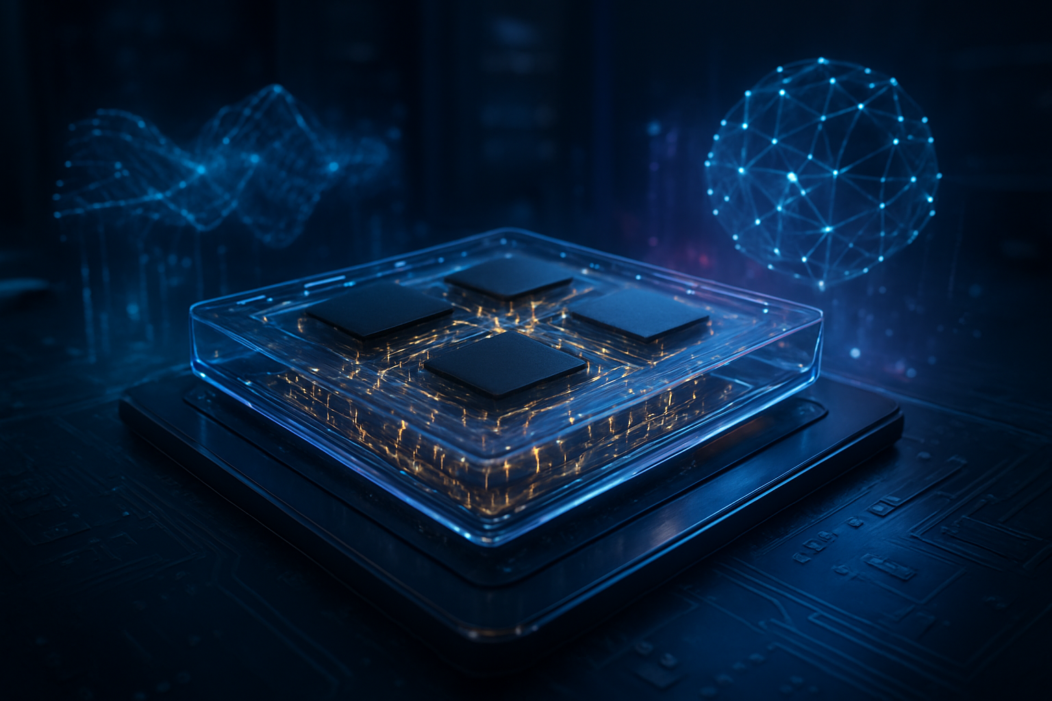
The Technical Breakdown: Overcoming the "Warpage Wall"
The move to glass is a response to the physical limitations of organic materials. Traditional ABF substrates, while reliable for decades, possess a Coefficient of Thermal Expansion (CTE) of roughly 15–17 ppm/°C. Silicon, by contrast, has a CTE of approximately 3 ppm/°C. As AI chips have grown larger and hotter, this mismatch has caused significant mechanical stress, leading to warped substrates and cracked solder bumps. Glass substrates solve this by offering a CTE of 3–5 ppm/°C, almost perfectly matching the silicon they support. This thermal stability allows for "reticle-busting" package sizes that can exceed 100mm x 100mm, accommodating dozens of chiplets and High Bandwidth Memory (HBM) stacks on a single, ultra-flat surface.
Beyond physical stability, glass offers transformative electrical properties. Unlike organic substrates, glass allows for a 10x increase in routing density through Through-Glass Vias (TGVs) with a pitch of less than 10μm. This density is essential for the massive data-transfer rates required for AI training. Furthermore, glass significantly reduces signal loss—by as much as 40% compared to ABF—improving overall power efficiency for data movement by up to 50%. This capability is vital as hyperscale data centers struggle with the energy demands of LLM (Large Language Model) inference and training.
Initial reactions from the AI research community have been overwhelmingly positive. Dr. Aris Gregorius, a lead packaging architect at the Silicon Valley Hardware Forum, noted that "glass is the only material capable of bridging the gap between current lithography limits and the multi-terawatt clusters of the future." Industry experts point out that while the transition is technically difficult, the success of Intel’s high-volume manufacturing (HVM) in Arizona proves that the manufacturing hurdles, such as glass brittleness and handling, have been successfully cleared.
A New Competitive Front: Intel, Samsung, and the South Korean Alliance
This technological shift has rearranged the competitive landscape of the semiconductor industry. Intel (NASDAQ: INTC) has secured a significant first-mover advantage, leveraging its advanced facility in Chandler, Arizona, to lead the charge. By integrating glass substrates into its Intel Foundry offerings, the company is positioning itself as the preferred partner for AI firms designing massive accelerators that traditional foundries struggle to package.
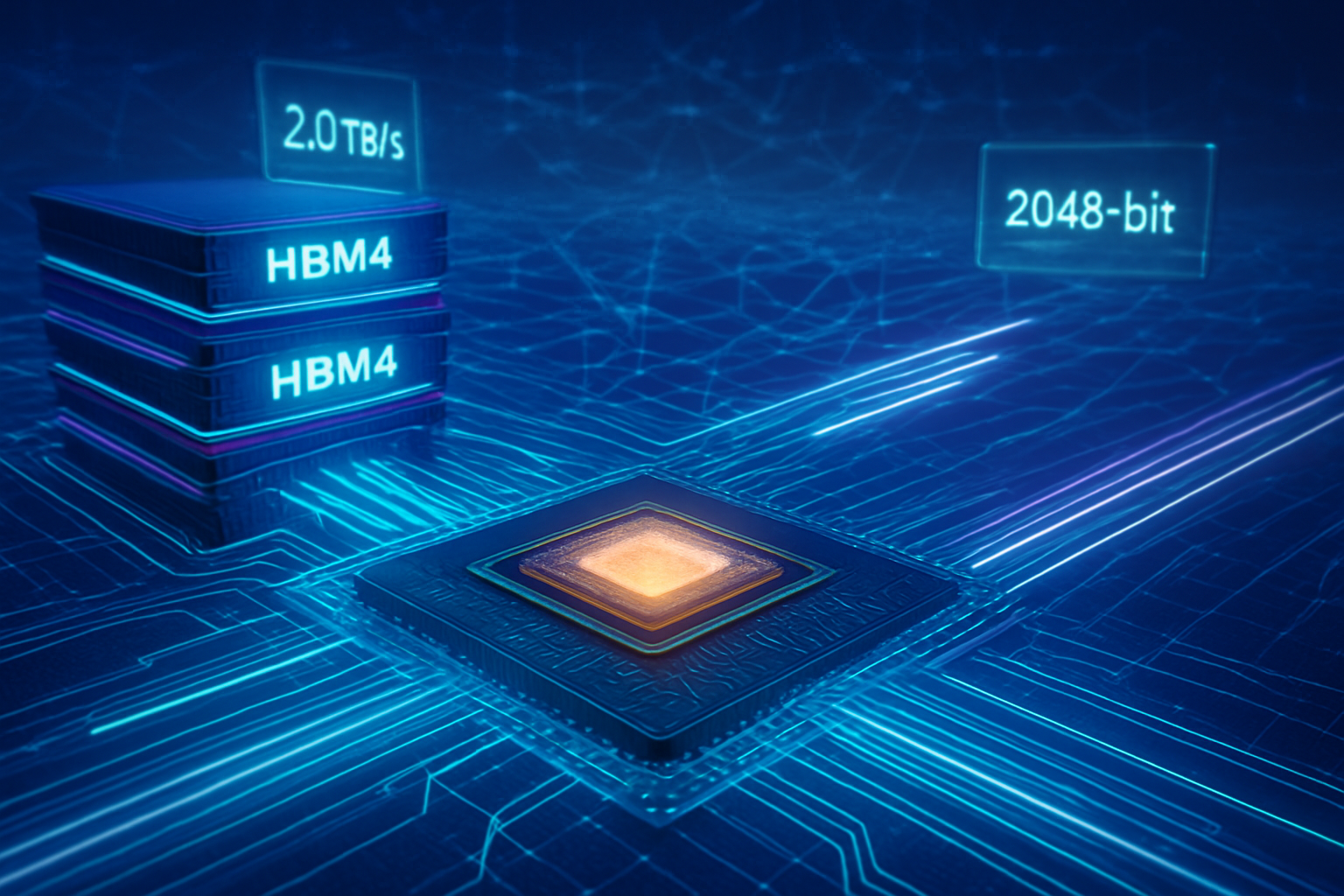
However, the competition is fierce. Samsung Electronics (KRX: 005930) has adopted a "One Samsung" strategy, combining the glass-handling expertise of Samsung Display with the chipmaking prowess of its foundry division. Samsung Electro-Mechanics has successfully moved its pilot line in Sejong, South Korea, into full-scale validation, with mass production targets set for the second half of 2026. This consolidated approach allows Samsung to offer an end-to-end solution, specifically focusing on glass interposers for the upcoming HBM4 memory standard.
Other major players are also making aggressive moves. Absolics, a subsidiary of SKC (KRX: 011790) backed by Applied Materials (NASDAQ: AMAT), has opened a state-of-the-art facility in Covington, Georgia. As of early 2026, Absolics is in the pre-qualification stage with AMD (NASDAQ: AMD) and Amazon (NASDAQ: AMZN) for custom AI hardware. Meanwhile, TSMC (NYSE: TSM) has accelerated its own Fan-Out Panel-Level Packaging (FO-PLP) on glass, partnering with Corning (NYSE: GLW) to develop specialized glass carriers that will eventually support its ubiquitous CoWoS (Chip-on-Wafer-on-Substrate) platform.
Broader Significance: The Future of AI Infrastructure
The industry-wide move to glass substrates is a clear indicator that the future of AI is no longer just about software algorithms, but about the physical limits of materials science. As we move deeper into 2026, the "Warpage Wall" has become the new frontier of Moore’s Law. By enabling larger, more densely packed chips, glass substrates allow for the continuation of performance scaling even as traditional transistor shrinking becomes prohibitively expensive and technically challenging.
This development also has significant implications for sustainability. The 50% improvement in power efficiency for data movement provided by glass substrates is a rare "green" win in an industry often criticized for its massive carbon footprint. By reducing the energy lost to heat and signal degradation, glass-based chips allow data centers to maximize their compute-per-watt, a metric that has become the primary KPI for major cloud providers.
There are, however, concerns regarding the supply chain. The transition requires a complete overhaul of packaging equipment and the development of new handling protocols for fragile glass panels. Some analysts worry that the initial high cost of glass substrates—currently 2-3 times that of ABF—could further widen the gap between tech giants who can afford the premium and smaller startups who may be priced out of the most advanced hardware.
Looking Ahead: Rectangular Panels and the Cost Curve
The next two to three years will likely be defined by the "Rectangular Revolution." While early glass substrates are being produced on 300mm round wafers, the industry is rapidly moving toward 600mm x 600mm rectangular panels. This transition is expected to drive costs down by 40-60% as the industry achieves the economies of scale necessary for mainstream adoption. Experts predict that by 2028, glass substrates will move beyond server-grade AI chips and into high-end consumer hardware, such as workstation-class laptops and gaming GPUs.
Challenges remain, particularly in the area of yield management. Inspecting for micro-cracks in a transparent substrate requires entirely new metrology tools, and the industry is currently racing to standardize these processes. Furthermore, China's BOE (SZSE: 000725) is entering the market with its own mass production targets for mid-2026, suggesting that a global trade battle over glass substrate capacity is likely on the horizon.
Summary: A Milestone in Computing History
The shift to glass substrates marks one of the most significant milestones in semiconductor packaging since the introduction of the flip-chip in the 1960s. By solving the thermal and mechanical limitations of organic materials, Intel, Samsung, and their peers have unlocked a new path for AI superchips, ensuring that the hardware can keep pace with the exponential growth of AI models.
As we look toward the coming months, the focus will shift to yield rates and the scaling of rectangular panel production. The "Glass Age" is no longer a futuristic concept; it is the current reality of the high-tech landscape, providing the literal foundation upon which the next decade of AI breakthroughs will be built.
This content is intended for informational purposes only and represents analysis of current AI developments.
TokenRing AI delivers enterprise-grade solutions for multi-agent AI workflow orchestration, AI-powered development tools, and seamless remote collaboration platforms.
For more information, visit https://www.tokenring.ai/.