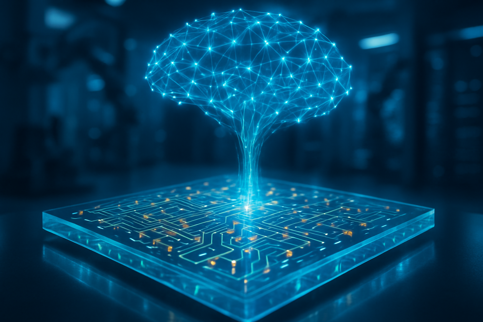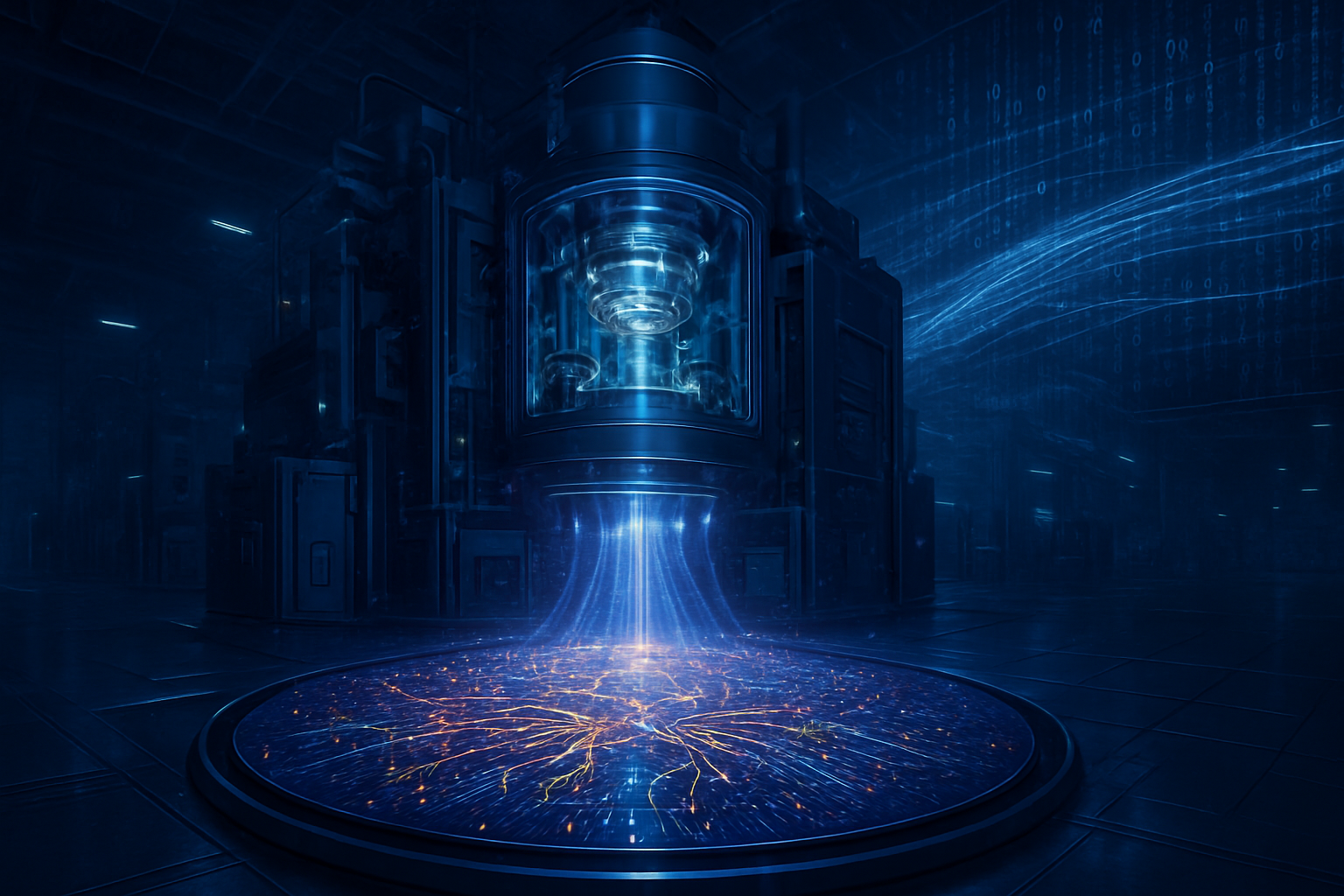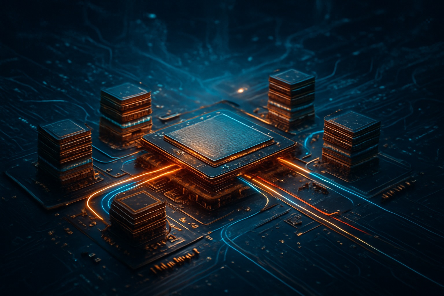
The semiconductor industry has officially entered the era of Backside Power Delivery (BSPDN), a fundamental architectural shift that marks the most significant change to transistor design in over a decade. As of January 2026, the long-promised "power wall" that threatened to stall AI progress is being dismantled, not by making transistors smaller, but by fundamentally re-engineering how they are powered. This breakthrough, which involves moving the intricate web of power circuitry from the top of the silicon wafer to its underside, is proving to be the secret weapon for the next generation of AI-ready processors.
The immediate significance of this development cannot be overstated. For years, chip designers have struggled with a "logistical nightmare" on the silicon surface, where power delivery wires and signal routing wires competed for the same limited space. This congestion led to significant electrical efficiency losses and restricted the density of logic gates. With the debut of Intel’s PowerVia and the upcoming arrival of TSMC’s Super Power Rail, the industry is seeing a leap in performance-per-watt that is essential for sustaining the massive computational demands of generative AI and large-scale inference models.
A Technical Deep Dive: PowerVia vs. Super Power Rail
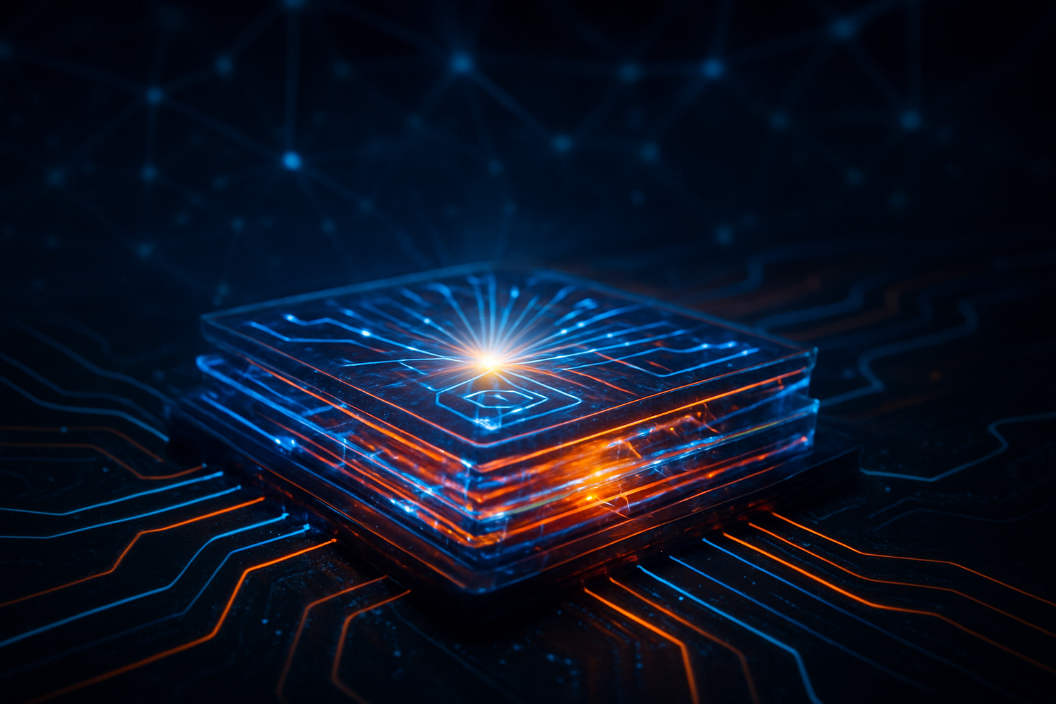
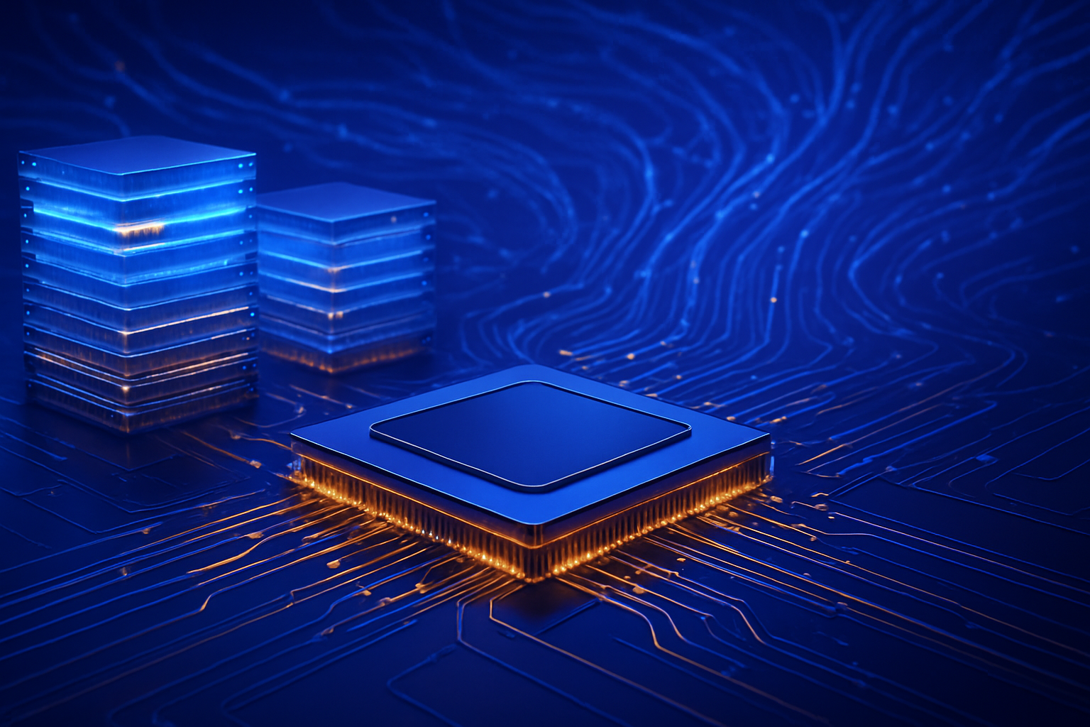
At the heart of this revolution are two competing implementations of BSPDN: PowerVia from Intel Corporation (NASDAQ: INTC) and the Super Power Rail (SPR) from Taiwan Semiconductor Manufacturing Company (NYSE: TSM). Intel has successfully taken the first-mover advantage, with its 18A node and Panther Lake processors hitting high-volume manufacturing in late 2025 and appearing in retail systems this month. Intel’s PowerVia utilizes Nano-Through Silicon Vias (nTSVs) to connect the power network on the back of the wafer to the transistors. This implementation has reduced IR drop—the voltage droop that occurs as electricity travels through a chip—from a standard 7% to less than 1%. By clearing the power lines from the frontside, Intel has achieved a staggering 30% increase in transistor density, allowing for more complex AI engines (NPUs) to be packed into smaller footprints.
TSMC is taking a more aggressive technical path with its Super Power Rail on the A16 node, scheduled for high-volume production in the second half of 2026. Unlike Intel’s nTSV approach, TSMC’s SPR connects the power network directly to the source and drain of the transistors. While significantly harder to manufacture, this "direct contact" method is expected to offer even higher electrical efficiency. TSMC projects that A16 will deliver a 15-20% power reduction at the same clock frequency compared to its 2nm (N2P) process. This approach is specifically engineered to handle the 1,000-watt power envelopes of future data center GPUs, effectively "shattering the performance wall" by allowing chips to sustain peak boost clocks without the electrical instability that plagued previous architectures.
Strategic Impacts on AI Giants and Startups
This shift in manufacturing technology is creating a new competitive landscape for AI companies. Intel’s early lead with PowerVia has allowed it to position its Panther Lake chips as the premier platform for "AI PCs," capable of running 70-billion-parameter LLMs locally on thin-and-light laptops. This poses a direct challenge to competitors who are still reliant on traditional frontside power delivery. For startups and independent AI labs, the increased density means that custom silicon—previously too expensive or complex to design—is becoming more viable, as BSPDN simplifies the physical design rules for high-performance logic.
Meanwhile, the anticipation for TSMC’s A16 node has already sparked a gold rush among the industry’s heavyweights. Nvidia (NASDAQ: NVDA) is reportedly the anchor customer for A16, intending to use the Super Power Rail to power its 2027 "Feynman" GPU architecture. The ability of A16 to deliver stable, high-amperage power directly to the transistor source is critical for Nvidia’s roadmap, which requires increasingly massive parallel throughput. For cloud giants like Amazon (NASDAQ: AMZN) and Google (NASDAQ: GOOGL), who are developing their own internal AI accelerators (Trainium and TPU), the choice between Intel’s available 18A and TSMC’s upcoming A16 will define their infrastructure efficiency and operational costs for the next three years.
The Broader Significance: Beyond Moore's Law
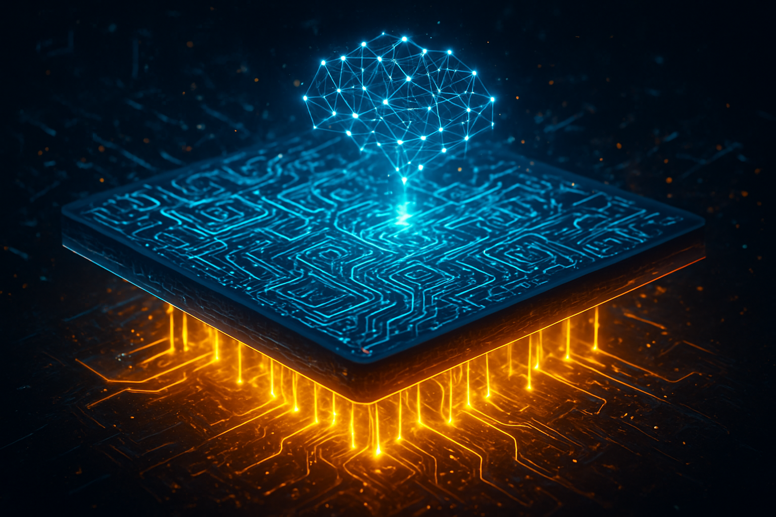
Backside Power Delivery represents more than just a clever engineering trick; it is a paradigm shift that extends the viability of Moore’s Law. As transistors shrunk toward the 2nm and 1.6nm scales, the "wiring bottleneck" became the primary limiting factor in chip performance. By separating the power and data highways into two distinct layers, the industry has effectively doubled the available "real estate" on the chip. This fits into the broader trend of "system-technology co-optimization" (STCO), where the physical structure of the chip is redesigned to meet the specific requirements of AI workloads, which are uniquely sensitive to latency and power fluctuations.
However, this transition is not without concerns. Moving power to the backside requires complex wafer-thinning and bonding processes that increase the risk of manufacturing defects. Thermal management also becomes more complex; while moving the power grid closer to the cooling solution can help, the extreme power density of these chips creates localized "hot spots" that require advanced liquid cooling or even diamond-based heat spreaders. Compared to previous milestones like the introduction of FinFET transistors, the move to BSPDN is arguably more disruptive because it changes the entire vertical stack of the semiconductor manufacturing process.
The Horizon: What Comes After 18A and A16?
Looking ahead, the successful deployment of BSPDN paves the way for the "1nm era" and beyond. In the near term, we expect to see "Backside Signal Routing," where not just power, but also some global clock and data signals are moved to the underside of the wafer to further reduce interference. Experts predict that by 2028, we will see the first true "3D-stacked" logic, where multiple layers of transistors are sandwiched between multiple layers of backside and frontside routing, leading to a ten-fold increase in AI compute density.
The primary challenge moving forward will be the cost of these advanced nodes. The equipment required for backside processing—specifically advanced wafer bonders and thinning tools—is incredibly expensive, which may lead to a widening gap between the "compute-rich" companies that can afford 1.6nm silicon and those stuck on older, frontside-powered nodes. As AI models continue to grow in size, the ability to manufacture these high-density, high-efficiency chips will become a matter of national economic security, further accelerating the "chip wars" between global superpowers.
Closing Thoughts on the BSPDN Era
The transition to Backside Power Delivery marks a historic moment in computing. Intel’s PowerVia has proven that the technology is ready for the mass market today, while TSMC’s Super Power Rail promises to push the boundaries of what is electrically possible by the end of the year. The key takeaway is that the "power wall" is no longer a fixed barrier; it is a challenge that has been solved through brilliant architectural innovation.
As we move through 2026, the industry will be watching the yields of TSMC’s A16 node and the adoption rates of Intel’s 18A-based Clearwater Forest Xeons. For the AI industry, these technical milestones translate directly into faster training times, more efficient inference, and the ability to run more sophisticated models on everyday devices. The silent revolution on the underside of the silicon wafer is, quite literally, powering the future of intelligence.
This content is intended for informational purposes only and represents analysis of current AI developments.
TokenRing AI delivers enterprise-grade solutions for multi-agent AI workflow orchestration, AI-powered development tools, and seamless remote collaboration platforms.
For more information, visit https://www.tokenring.ai/.