Tag: AI Hardware

  • The $380 Million Gamble: Intel Seizes the Lead in the Angstrom Era with High-NA EUV

    The $380 Million Gamble: Intel Seizes the Lead in the Angstrom Era with High-NA EUV

    As of January 13, 2026, the global semiconductor landscape has reached a historic inflection point. Intel Corp (NASDAQ: INTC) has officially transitioned its 18A (1.8-nanometer) process node into High-Volume Manufacturing (HVM), marking the first time in over a decade that the American chipmaker has arguably leapfrogged its primary rivals in manufacturing technology. This milestone is underpinned by the strategic deployment of High Numerical Aperture (High-NA) Extreme Ultraviolet (EUV) lithography, a revolutionary printing technique that allows for unprecedented transistor density and precision.

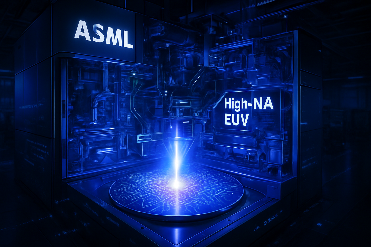
    The immediate significance of this development cannot be overstated. By being the first to integrate ASML Holding (NASDAQ: ASML) Twinscan EXE:5200B scanners into its production lines, Intel is betting that it can overcome the "yield wall" that has plagued sub-2nm development. While competitors have hesitated due to the astronomical costs of the new hardware, Intel’s early adoption is already bearing fruit, with the company reporting stable 18A yields that have cleared the 65% threshold—making mass-market production of its next-generation "Panther Lake" and "Clearwater Forest" processors economically viable.

    Precision at the Atomic Scale: The 0.55 NA Advantage

    The technical leap from standard EUV to High-NA EUV is defined by the increase in numerical aperture from 0.33 to 0.55. This shift allows the ASML Twinscan EXE:5200B to achieve a resolution of just 8nm, a massive improvement over the 13.5nm limit of previous-generation machines. In practical terms, this enables Intel to print features that are 1.7x smaller than before, contributing to a nearly 2.9x increase in overall transistor density. For the first time, engineers are working with tolerances where a single stray atom can determine the success or failure of a logic gate.

    Unlike previous approaches that required complex "multi-patterning"—where a single layer of a chip is printed multiple times to achieve the desired resolution—High-NA EUV allows for single-exposure patterning of the most critical layers. This reduction in process steps is the secret weapon behind Intel’s yield improvements. By eliminating the cumulative errors inherent in multi-patterning, Intel has managed to improve its 18A yields by approximately 7% month-over-month throughout late 2025. The new scanners also boast a record-breaking 0.7nm overlay accuracy, ensuring that the dozens of atomic-scale layers in a modern processor are aligned with near-perfect precision.

    Initial reactions from the semiconductor research community have been a mix of awe and cautious optimism. Analysts at major firms have noted that while the transition to High-NA involves a "half-field" mask size—effectively halving the area a scanner can print in one go—the EXE:5200B’s throughput of 175 to 200 wafers per hour mitigates the potential productivity loss. The industry consensus is that Intel has successfully navigated the steepest part of the learning curve, gaining operational knowledge that its competitors have yet to even begin acquiring.

    A $380 Million Barrier to Entry: Shifting Industry Dynamics

    The primary deterrent for High-NA adoption has been the staggering price tag: approximately $380 million (€350 million) per machine. This cost represents more than just the hardware; it includes a massive logistical tail, requiring specialized fab cleanrooms and a six-month installation period led by hundreds of ASML engineers. Intel’s decision to purchase the lion's share of ASML's early production run has created a temporary monopoly on the most advanced manufacturing capacity in the world, effectively building a "moat" made of capital and specialized expertise.

    This strategy has placed Taiwan Semiconductor Manufacturing Company (NYSE: TSM) in an uncharacteristically defensive position. TSMC has opted to extend its existing 0.33 NA tools for its A14 node, utilizing advanced multi-patterning to avoid the high capital expenditure of High-NA. While this conservative approach protects TSMC’s short-term margins, it leaves them trailing Intel in High-NA operational experience by an estimated 24 months. Meanwhile, Samsung Electronics (KRX: 005930) continues to struggle with yield issues on its 2nm Gate-All-Around (GAA) process, further delaying its own High-NA roadmap until at least 2028.

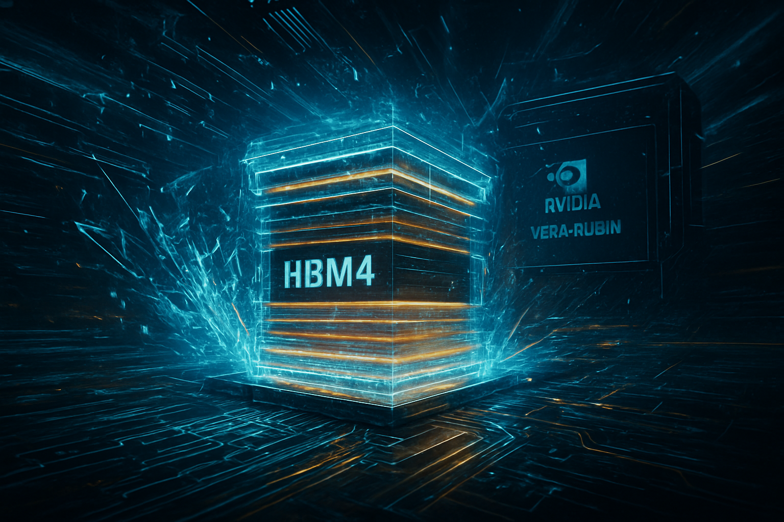
    For AI companies and tech giants, Intel’s resurgence offers a vital second source for cutting-edge silicon. As the demand for AI accelerators and high-performance computing (HPC) chips continues to outpace supply, Intel’s Foundry services are becoming an attractive alternative to TSMC. By providing a "High-NA native" path for its upcoming 14A node, Intel is positioning itself as the premier partner for the next generation of AI hardware, potentially disrupting the long-standing dominance of the "TSMC-only" supply chain for top-tier silicon.

    Sustaining Moore’s Law in the AI Era

    The deployment of High-NA EUV is more than just a corporate victory for Intel; it is a vital sign for the longevity of Moore’s Law. As the industry moved toward the 2nm limit, many feared that the physical and economic barriers of lithography would bring the era of rapid transistor scaling to an end. High-NA EUV effectively resets the clock, providing a clear technological roadmap into the 1nm (10 Angstrom) range and beyond. This fits into a broader trend where the "Angstrom Era" is defined not just by smaller transistors, but by the integration of advanced packaging and backside power delivery—technologies like Intel’s PowerVia that work in tandem with High-NA lithography.

    However, the wider significance of this milestone also brings potential concerns regarding the "geopolitics of silicon." With High-NA tools being so expensive and rare, the gap between the "haves" and the "have-nots" in the semiconductor world is widening. Only a handful of companies—and by extension, a handful of nations—can afford to participate at the leading edge. This concentration of power could lead to increased market volatility if supply chain disruptions occur at the few sites capable of housing these $380 million machines.

    Compared to previous milestones, such as the initial introduction of EUV in 2019, the High-NA transition has been remarkably focused on the US-based manufacturing footprint. Intel’s primary High-NA operations are centered in Oregon and Arizona, signaling a significant shift in the geographical concentration of advanced chipmaking. This alignment with domestic manufacturing goals has provided Intel with a strategic tailwind, as Western governments prioritize the resilience of high-end semiconductor supplies for AI and national security.

    The Road to 14A and Beyond

    Looking ahead, the next two to three years will be defined by the maturation of the 14A (1.4nm) node. While 18A uses a "hybrid" approach with High-NA applied only to the most critical layers, the 14A node is expected to be "High-NA native," utilizing the technology across a much broader range of the chip’s architecture. Experts predict that by 2027, the operational efficiencies gained from High-NA will begin to lower the cost-per-transistor once again, potentially sparking a new wave of innovation in consumer electronics and edge-AI devices.

    One of the primary challenges remaining is the evolution of the mask and photoresist ecosystem. High-NA requires thinner resists and more complex mask designs to handle the higher angles of light. ASML and its partners are already working on the next iteration of the EXE platform, with rumors of "Hyper-NA" (0.75 NA) already circulating in R&D circles for the 2030s. For now, the focus remains on perfecting the 18A ramp and ensuring that the massive capital investment in High-NA translates into sustained market share gains.

    Predicting the next move, industry analysts expect TSMC to accelerate its High-NA evaluation as Intel’s 18A products hit the shelves. If Intel’s "Panther Lake" processors demonstrate a significant performance-per-watt advantage, the pressure on TSMC to abandon its conservative stance will become overwhelming. The "Lithography Wars" are far from over, but in early 2026, Intel has clearly seized the high ground.

    Conclusion: A New Leader in the Silicon Race

    The strategic deployment of High-NA EUV lithography in 2026 marks the beginning of a new chapter in semiconductor history. Intel’s willingness to shoulder the $380 million cost of early adoption has paid off, providing the company with a 24-month head start in the most critical manufacturing technology of the decade. With 18A yields stabilizing and high-volume manufacturing underway, the "Angstrom Era" is no longer a theoretical roadmap—it is a production reality.

    The key takeaway for the industry is that the "barrier to entry" at the leading edge has been raised to unprecedented heights. The combination of extreme capital requirements and the steep learning curve of 0.55 NA optics has created a bifurcated market. Intel’s success in reclaiming the manufacturing "crown" will be measured not just by the performance of its own chips, but by its ability to attract major foundry customers who are hungry for the density and efficiency that only High-NA can provide.

    In the coming months, all eyes will be on the first third-party benchmarks of Intel 18A silicon. If these chips deliver on their promises, the shift in the balance of power from East to West may become a permanent fixture of the tech landscape. For now, Intel’s $380 million gamble looks like the smartest bet in the history of the industry.


    This content is intended for informational purposes only and represents analysis of current AI developments.

    TokenRing AI delivers enterprise-grade solutions for multi-agent AI workflow orchestration, AI-powered development tools, and seamless remote collaboration platforms.
    For more information, visit https://www.tokenring.ai/.

  • The HBM4 Memory War: SK Hynix, Samsung, and Micron Battle for AI Supremacy at CES 2026

    The HBM4 Memory War: SK Hynix, Samsung, and Micron Battle for AI Supremacy at CES 2026

    The floor of CES 2026 has transformed into a high-stakes battlefield for the semiconductor industry, as the "HBM4 Memory War" officially ignited among the world’s three largest memory manufacturers. With the artificial intelligence revolution entering a new phase of massive-scale model training, the demand for High Bandwidth Memory (HBM) has shifted from a supply-chain bottleneck to the primary architectural hurdle for next-generation silicon. The announcements made this week by SK Hynix, Samsung, and Micron represent more than just incremental speed bumps; they signal a fundamental shift in how memory and logic are integrated to power the most advanced AI clusters on the planet.

    This surge in memory innovation is being driven by the arrival of NVIDIA’s (NASDAQ:NVDA) new "Vera Rubin" architecture, the much-anticipated successor to the Blackwell platform. As AI models grow to tens of trillions of parameters, the industry has hit the "memory wall"—a physical limit where processors are fast enough to compute data, but the memory cannot feed it to them quickly enough. HBM4 is the industry's collective answer to this crisis, offering the massive bandwidth and energy efficiency required to prevent the world’s most expensive GPUs from sitting idle while waiting for data.

    The 16-Layer Breakthrough and the 1c Efficiency Edge

    At the center of the CES hardware showcase, SK Hynix (KRX:000660) stunned the industry by debuting the world’s first 16-layer (16-Hi) 48GB HBM4 stack. This engineering marvel doubles the density of previous generations while maintaining a strict 775µm height limit required by standard packaging. To achieve this, SK Hynix thinned individual DRAM wafers to just 30 micrometers—roughly one-third the thickness of a human hair—using its proprietary Advanced Mass Reflow Molded Underfill (MR-MUF) technology. The result is a single memory cube capable of an industry-leading 11.7 Gbps per pin, providing the sheer density needed for the ultra-large language models expected in late 2026.

    Samsung Electronics (KRX:005930) took a different strategic path, emphasizing its "one-stop shop" capability and manufacturing efficiency. Samsung’s HBM4 is built on its cutting-edge 1c (6th generation 10nm-class) DRAM process, which the company claims offers a 40% improvement in energy efficiency over current 1b-based modules. Unlike its competitors, Samsung is leveraging its internal foundry to produce both the memory and the logic base die, aiming to provide a more integrated and cost-effective solution. This vertical integration is a direct challenge to the partnership-driven models of its rivals, positioning Samsung as a turnkey provider for the HBM4 era.

    Not to be outdone, Micron Technology (NASDAQ:MU) announced an aggressive $20 billion capital expenditure plan for the coming fiscal year to fuel its capacity expansion. Micron’s HBM4 entry focuses on a 12-layer 36GB stack that utilizes a 2,048-bit interface—double the width of the HBM3E standard. By widening the data "pipe," Micron is achieving speeds exceeding 2.0 TB/s per stack. The company is rapidly scaling its "megaplants" in Taiwan and Japan, aiming to capture a significantly larger slice of the HBM market share, which SK Hynix has dominated for the past two years.

    Fueling the Rubin Revolution and Redefining Market Power

    The immediate beneficiary of this memory arms race is NVIDIA, whose Vera Rubin GPUs are designed to utilize eight stacks of HBM4 memory. With SK Hynix’s 48GB stacks, a single Rubin GPU could boast a staggering 384GB of high-speed memory, delivering an aggregate bandwidth of 22 TB/s. This is a nearly 3x increase over the Blackwell architecture, allowing for real-time inference of models that previously required entire server racks. The competitive implications are clear: the memory maker that can provide the highest yield of 16-layer stacks will likely secure the lion's share of NVIDIA's multi-billion dollar orders.

    For the broader tech landscape, this development creates a new hierarchy. Companies like Advanced Micro Devices (NASDAQ:AMD) are also pivoting their Instinct accelerator roadmaps to support HBM4, ensuring that the "memory war" isn't just an NVIDIA-exclusive event. However, the shift to HBM4 also elevates the importance of Taiwan Semiconductor Manufacturing Company (NYSE:TSM), which is collaborating with SK Hynix and Micron to manufacture the logic base dies that sit at the bottom of the HBM stack. This "foundry-memory" alliance is a direct competitive response to Samsung's internal vertical integration, creating two distinct camps in the semiconductor world: the specialists versus the integrated giants.

    Breaking the Memory Wall and the Shift to Logic-Integrated Memory

    The wider significance of HBM4 lies in its departure from traditional memory design. For the first time, the base die of the memory stack—the foundation upon which the DRAM layers sit—is being manufactured using advanced logic nodes (such as 5nm or 4nm). This effectively turns the memory stack into a "co-processor." By moving some of the data pre-processing and memory management directly into the HBM4 stack, engineers can reduce the energy-intensive data movement between the GPU and the memory, which currently accounts for a significant portion of a data center’s power consumption.

    This evolution is the most significant step yet in overcoming the "Memory Wall." In previous generations, the gap between compute speed and memory bandwidth was widening at an exponential rate. HBM4’s 2,048-bit interface and logic-integrated base die finally provide a roadmap to close that gap. This is not just a hardware upgrade; it is a fundamental rethinking of computer architecture that moves us closer to "near-memory computing," where the lines between where data is stored and where it is processed begin to blur.

    The Horizon: Custom HBM and the Path to HBM5

    Looking ahead, the next phase of this war will be fought on the ground of "Custom HBM" (cHBM). Experts at CES 2026 predict that by 2027, major AI players like Google or Amazon may begin commissioning HBM stacks with logic dies specifically designed for their own proprietary AI chips. This level of customization would allow for even greater efficiency gains, potentially tailoring the memory's internal logic to the specific mathematical operations required by a company's unique neural network architecture.

    The challenges remaining are largely thermal and yield-related. Stacking 16 layers of DRAM creates immense heat density, and the precision required to align thousands of Through-Silicon Vias (TSVs) across 16 layers is unprecedented. If yields on these 16-layer stacks remain low, the industry may see a prolonged period of supply shortages, keeping the price of AI compute high despite the massive capacity expansions currently underway at Micron and Samsung.

    A New Chapter in AI History

    The HBM4 announcements at CES 2026 mark a definitive turning point in the AI era. We have moved past the phase where raw FLOPs (Floating Point Operations per Second) were the only metric that mattered. Today, the ability to store, move, and access data at the speed of thought is the true measure of AI performance. The "Memory War" between SK Hynix, Samsung, and Micron is a testament to the critical role that specialized hardware plays in the advancement of artificial intelligence.

    In the coming weeks, the industry will be watching for the first third-party benchmarks of the Rubin architecture and the initial yield reports from the new HBM4 production lines. As these components begin to ship to data centers later this year, the impact will be felt in everything from the speed of scientific research to the capabilities of consumer-facing AI agents. The HBM4 era has arrived, and it is the high-octane fuel that will power the next decade of AI innovation.


    This content is intended for informational purposes only and represents analysis of current AI developments.

    TokenRing AI delivers enterprise-grade solutions for multi-agent AI workflow orchestration, AI-powered development tools, and seamless remote collaboration platforms.
    For more information, visit https://www.tokenring.ai/.

  • NVIDIA Unveils Vera Rubin Platform at CES 2026: A 10x Leap Toward the Era of Agentic AI

    NVIDIA Unveils Vera Rubin Platform at CES 2026: A 10x Leap Toward the Era of Agentic AI

    LAS VEGAS — In a landmark presentation at CES 2026, NVIDIA (NASDAQ: NVDA) has officially ushered in the next epoch of computing with the launch of the Vera Rubin platform. Named after the legendary astronomer who provided the first evidence of dark matter, the platform represents a total architectural overhaul designed to solve the most pressing bottleneck in modern technology: the transition from passive generative AI to autonomous, reasoning "agentic" AI.

    The announcement, delivered by CEO Jensen Huang to a capacity crowd, centers on a suite of six new chips that function as a singular, cohesive AI supercomputer. By integrating compute, networking, and memory at an unprecedented scale, NVIDIA claims the Vera Rubin platform will reduce AI inference costs by a factor of 10, effectively commoditizing high-level reasoning for enterprises and consumers alike.

    The Six Pillars of Rubin: A Masterclass in Extreme Codesign

    The Vera Rubin platform is built upon six foundational silicon advancements that NVIDIA describes as "extreme codesign." At the heart of the system is the Rubin GPU, a behemoth featuring 336 billion transistors and 288 GB of HBM4 memory. Delivering a staggering 22 TB/s of memory bandwidth per socket, the Rubin GPU is engineered to handle the massive Mixture-of-Experts (MoE) models that define the current state-of-the-art. Complementing the GPU is the Vera CPU, which marks a departure from traditional general-purpose processing. Featuring 88 custom "Olympus" cores compatible with Arm (NASDAQ: ARM) v9.2 architecture, the Vera CPU acts as a dedicated "data movement engine" optimized for the iterative logic and multi-step reasoning required by AI agents.

    The interconnect and networking stack has seen an equally dramatic upgrade. NVLink 6 doubles scale-up bandwidth to 3.6 TB/s per GPU, allowing a rack of 72 GPUs to act as a single, massive processor. On the scale-out side, the ConnectX-9 SuperNIC and Spectrum-6 Ethernet switch provide 1.6 Tb/s and 102.4 Tb/s of throughput, respectively, with the latter utilizing Co-Packaged Optics (CPO) for a 5x improvement in power efficiency. Finally, the BlueField-4 DPU introduces a dedicated Inference Context Memory Storage Platform, offloading Key-Value (KV) cache management to improve token throughput by 5x, effectively giving AI models a "long-term memory" during complex tasks.

    Microsoft and the Rise of the Fairwater AI Superfactories

    The immediate commercial impact of the Vera Rubin platform is being realized through a massive strategic partnership with Microsoft Corp. (NASDAQ: MSFT). Microsoft has been named the premier launch partner, integrating the Rubin architecture into its new "Fairwater" AI superfactories. These facilities, located in strategic hubs like Wisconsin and Atlanta, are designed to house hundreds of thousands of Vera Rubin Superchips in a unique three-dimensional rack configuration that minimizes cable runs and maximizes the efficiency of the NVLink 6 fabric.

    This partnership is a direct challenge to the broader cloud infrastructure market. By achieving a 10x reduction in inference costs, Microsoft and NVIDIA are positioning themselves to dominate the "agentic" era, where AI is not just a chatbot but a persistent digital employee performing complex workflows. For startups and competing AI labs, the Rubin platform raises the barrier to entry; training a 10-trillion parameter model now takes 75% fewer GPUs than it did on the previous Blackwell architecture. This shift effectively forces competitors to either adopt NVIDIA’s proprietary stack or face a massive disadvantage in both speed-to-market and operational cost.

    From Chatbots to Agents: The Reasoning Era

    The broader significance of the Vera Rubin platform lies in its explicit focus on "Agentic AI." While the previous generation of hardware was optimized for the "training era"—ingesting vast amounts of data to predict the next token—Rubin is built for the "reasoning era." This involves agents that can plan, use tools, and maintain context over weeks or months of interaction. The hardware-accelerated adaptive compression and the BlueField-4’s context management are specifically designed to handle the "long-context" requirements of these agents, allowing them to remember previous interactions and complex project requirements without the massive latency penalties of earlier systems.

    This development mirrors the historical shift from mainframe computing to the PC, or from the desktop to mobile. By making high-level reasoning 10 times cheaper, NVIDIA is enabling a world where every software application can have a dedicated, autonomous agent. However, this leap also brings concerns regarding the energy consumption of such massive clusters and the potential for rapid job displacement as AI agents become capable of handling increasingly complex white-collar tasks. Industry experts note that the Rubin platform is not just a faster chip; it is a fundamental reconfiguration of how data centers are built and how software is conceived.

    The Road Ahead: Robotics and Physical AI

    Looking toward the future, the Vera Rubin platform is expected to serve as the backbone for NVIDIA’s expansion into "Physical AI." The same architectural breakthroughs found in the Vera CPU and Rubin GPU are already being adapted for the GR00T humanoid robotics platform and the Alpamayo autonomous driving system. In the near term, we can expect the first Fairwater-powered agentic services to roll out to Microsoft Azure customers by the second half of 2026.

    The long-term challenge for NVIDIA will be managing the sheer power density of these systems. With the Rubin NVL72 requiring advanced liquid cooling and specialized power delivery, the infrastructure requirements for the "AI Superfactory" are becoming as complex as the silicon itself. Nevertheless, analysts predict that the Rubin platform will remain the gold standard for AI compute for the remainder of the decade, as the industry moves away from static models toward dynamic, self-improving agents.

    A New Benchmark in Computing History

    The launch of the Vera Rubin platform at CES 2026 is more than a routine product update; it is a declaration of the "Reasoning Era." By unifying six distinct chips into a singular, liquid-cooled fabric, NVIDIA has redefined the limits of what is possible in silicon. The 10x reduction in inference cost and the massive-scale partnership with Microsoft ensure that the Vera Rubin architecture will be the foundation upon which the next generation of autonomous digital and physical systems are built.

    As we move into the second half of 2026, the tech industry will be watching closely to see how the first Fairwater superfactories perform and how quickly agentic AI can be integrated into the global economy. For now, Jensen Huang and NVIDIA have once again set a pace that the rest of the industry must struggle to match, proving that in the race for AI supremacy, the hardware remains the ultimate gatekeeper.


    This content is intended for informational purposes only and represents analysis of current AI developments.

    TokenRing AI delivers enterprise-grade solutions for multi-agent AI workflow orchestration, AI-powered development tools, and seamless remote collaboration platforms.
    For more information, visit https://www.tokenring.ai/.

  • The Open Silicon Revolution: RISC-V Reaches Maturity, Challenging the ARM and x86 Duopoly

    The Open Silicon Revolution: RISC-V Reaches Maturity, Challenging the ARM and x86 Duopoly

    As of January 12, 2026, the global semiconductor landscape has reached a historic inflection point. The RISC-V architecture, once a niche academic project, has officially matured into the "third pillar" of computing, standing alongside the long-dominant x86 and ARM architectures. With a global market penetration of 25% in silicon unit shipments and the recent ratification of the RVA23 standard, RISC-V is no longer just an alternative for low-power microcontrollers; it has become a formidable contender in the high-performance data center and AI markets.

    This shift represents a fundamental change in how the world builds and licenses technology. Driven by a global demand for "silicon sovereignty" and an urgent need for licensing-free chip designs in the face of escalating geopolitical tensions, RISC-V has moved from the periphery to the center of strategic planning for tech giants and sovereign nations alike. The recent surge in adoption signals a move away from the restrictive, royalty-heavy models of the past toward an open-source future where hardware customization is the new standard.

    The Technical Ascent: From Microcontrollers to "Brawny" Cores

    The technical maturity of RISC-V in 2026 is anchored by the transition to "brawny" high-performance cores that rival the best from Intel (NASDAQ: INTC) and ARM (NASDAQ: ARM). A key milestone was the late 2025 launch of Tenstorrent’s Ascalon-X CPU. Designed under the leadership of industry legend Jim Keller, the Ascalon-X is an 8-wide decode, out-of-order core that has demonstrated performance parity with AMD’s (NASDAQ: AMD) Zen 5 in single-threaded IPC (Instructions Per Cycle). This development has silenced critics who once argued that an open-source ISA could never achieve the raw performance required for modern server workloads.

    Central to this technical evolution is the RVA23 profile ratification, which has effectively ended the "Wild West" era of RISC-V fragmentation. By mandating a standardized set of extensions—including Vector 1.0, Hypervisor, and Bitmanip—RVA23 ensures that software developed for one RISC-V chip will run seamlessly on another. This has cleared the path for major operating systems like Ubuntu 26.04 and Red Hat Enterprise Linux 10 to provide full, tier-one support for the architecture. Furthermore, Google (NASDAQ: GOOGL) has elevated RISC-V to a Tier 1 supported platform for Android, paving the way for a new generation of mobile devices and wearables.

    In the realm of Artificial Intelligence, RISC-V is leveraging its inherent flexibility to outperform traditional architectures. The finalized RISC-V Vector (RVV) and Matrix extensions allow developers to handle both linear algebra and complex activation functions on the same silicon, eliminating the bottlenecks often found in dedicated NPUs. Hardware from companies like Alibaba (NYSE: BABA) and the newly reorganized Esperanto IP (now under Ainekko) now natively supports BF16 and FP8 data types, which are essential for the "Mixture-of-Experts" (MoE) models that dominate the 2026 AI landscape.

    Initial reactions from the research community have been overwhelmingly positive, with experts noting that RISC-V’s 30–40% better Power-Performance-Area (PPA) metrics compared to ARM in custom chiplet configurations make it the ideal choice for the next generation of "right-sized" AI math. The ability to modify the RTL (Register Transfer Level) source code allows companies to strip away legacy overhead, creating leaner, more efficient processors specifically tuned for LLM inference.

    A Market in Flux: Hyperscalers and the "De-ARMing" of the Industry

    The market implications of RISC-V’s maturity are profound, causing a strategic realignment among the world's largest technology companies. In a move that sent shockwaves through the industry in December 2025, Qualcomm (NASDAQ: QCOM) acquired Ventana Micro Systems for $2.4 billion. This acquisition is widely viewed as a strategic hedge against Qualcomm’s ongoing legal and royalty disputes with ARM, signaling a "second path" for the mobile chip giant that prioritizes open-source IP over proprietary licenses.

    Hyperscalers are also leading the charge. Meta (NASDAQ: META), following its acquisition of Rivos, has integrated custom RISC-V cores into its data center roadmap to power its Llama-class large language models. By using RISC-V, Meta can design chips that are perfectly tailored to its specific AI workloads, avoiding the "ARM tax" and reducing its reliance on off-the-shelf solutions from NVIDIA (NASDAQ: NVDA). Similarly, Google’s RISE (RISC-V Software Ecosystem) project has matured, providing a robust development environment that allows cloud providers to build their own custom silicon fabrics with RISC-V cores at the heart.

    The competitive landscape is now defined by a struggle for "silicon sovereignty." For major AI labs and tech companies, the strategic advantage of RISC-V lies in its total customizability. Unlike the "black box" approach of NVIDIA or the fixed roadmaps of ARM, RISC-V allows for total RTL modification. This enables startups and established giants to innovate at the architectural level, creating proprietary extensions for specialized tasks like graph processing or encrypted computing without needing permission from a central licensing authority.

    This shift is already disrupting existing product lines. In the wearable market, the first mass-market RISC-V Android SoCs have begun to displace ARM-based designs, offering better battery life and lower costs. In the data center, Tenstorrent's "Innovation License" model—which provides the source code for its cores to partners like Samsung (KRX: 005930) and Hyundai—is challenging the traditional vendor-customer relationship, turning hardware consumers into hardware co-creators.

    Geopolitics and the Drive for Self-Sufficiency

    Beyond the technical and market shifts, the rise of RISC-V is inextricably linked to the global geopolitical climate. For China, RISC-V has become the cornerstone of its national drive for semiconductor self-sufficiency. Under the "Eight-Agency" policy released in March 2025, Beijing has coordinated a nationwide push to adopt the architecture, aiming to bypass U.S. export controls and the restrictive licensing regimes of Western proprietary standards.

    The open-source nature of RISC-V provides a "geopolitically neutral" pathway. Because RISC-V International is headquartered in Switzerland, the core Instruction Set Architecture (ISA) remains outside the direct jurisdiction of the U.S. Department of Commerce. This has allowed Chinese firms like Alibaba’s T-Head and the Beijing Institute of Open Source Chip (BOSC) to develop high-performance cores like the Xiangshan (Kunminghu)—which now performs within 8% of the ARM Neoverse N2—without the fear of having their licenses revoked.

    This "de-Americanization" of the supply chain is not limited to China. European initiatives are also exploring RISC-V as a way to reduce dependence on foreign technology and foster a domestic semiconductor ecosystem. The concept of "Silicon Sovereignty" has become a rallying cry for nations that want to ensure their critical infrastructure is built on open, auditable, and perpetual standards. RISC-V is the only architecture that meets these criteria, making it a vital tool for national security and economic resilience.

    However, this shift also raises concerns about the potential for a "splinternet" of hardware. While the RVA23 profile provides a baseline for compatibility, there is a risk that different geopolitical blocs could develop mutually incompatible extensions, leading to a fragmented global tech landscape. Despite these concerns, the momentum behind RISC-V suggests that the benefits of an open, royalty-free standard far outweigh the risks of fragmentation, especially as the world moves toward a more multi-polar technological order.

    The Horizon: Sub-3nm Nodes and the Windows Frontier

    Looking ahead, the next 24 months will see RISC-V push into even more demanding environments. The roadmap for 2026 and 2027 includes the transition to sub-3nm manufacturing nodes, with companies like Tenstorrent and Ventana planning "Babylon" and "Veyron V3" chips that focus on extreme compute density and multi-chiplet scaling. These designs are expected to target the most intensive AI training workloads, directly challenging NVIDIA's dominance in the frontier model space.

    One of the most anticipated developments is the arrival of "Windows on RISC-V." While Microsoft (NASDAQ: MSFT) has already demonstrated developer versions of Windows 11 running on the architecture, a full consumer release is expected within the next two to three years. This would represent the final hurdle for RISC-V, allowing it to compete in the high-end laptop and desktop markets that are currently the stronghold of x86 and ARM. The success of this transition will depend on the maturity of "Prism"-style emulation layers to run legacy x86 applications.

    In addition to PCs, the automotive and edge AI sectors are poised for a RISC-V takeover. The architecture’s inherent efficiency and the ability to integrate custom safety and security extensions make it a natural fit for autonomous vehicles and industrial robotics. Experts predict that by 2028, RISC-V could become the dominant architecture for new automotive designs, as carmakers seek to build their own software-defined vehicles without being tied to a single chip vendor's roadmap.

    A New Era for Global Computing

    The maturity of RISC-V marks the end of the decades-long duopoly of ARM and x86. By providing a high-performance, royalty-free, and fully customizable alternative, RISC-V has democratized silicon design and empowered a new generation of innovators. From the data centers of Silicon Valley to the research hubs of Shanghai, the architecture is being used to build more efficient, more specialized, and more secure computing systems.

    The significance of this development in the history of AI cannot be overstated. As AI models become more complex and power-hungry, the ability to "right-size" hardware through an open-source ISA is becoming a critical competitive advantage. RISC-V has proven that the open-source model, which revolutionized the software world through Linux, is equally capable of transforming the hardware world.

    In the coming weeks and months, the industry will be watching closely as the first RVA23-compliant server chips begin mass deployment and as the mobile ecosystem continues its steady migration toward open silicon. The "Open Silicon Revolution" is no longer a future possibility—it is a present reality, and it is reshaping the world one instruction at a time.


    This content is intended for informational purposes only and represents analysis of current AI developments.

    TokenRing AI delivers enterprise-grade solutions for multi-agent AI workflow orchestration, AI-powered development tools, and seamless remote collaboration platforms.
    For more information, visit https://www.tokenring.ai/.

  • Intel’s 18A “Power-On” Milestone: A High-Stakes Gamble to Reclaim the Silicon Throne

    Intel’s 18A “Power-On” Milestone: A High-Stakes Gamble to Reclaim the Silicon Throne

    As of January 12, 2026, the global semiconductor landscape stands at a historic crossroads. Intel Corporation (NASDAQ: INTC) has officially confirmed the successful "powering on" and initial mass production of its 18A (1.8nm) process node, a milestone that many analysts are calling the most significant event in the company’s 58-year history. This achievement marks the first time in nearly a decade that Intel has a credible claim to the "leadership" title in transistor performance, arriving just as the company fights to recover from a bruising 2025 where its global semiconductor market share plummeted to a record low of 6%.

    The 18A node is not merely a technical update; it is the linchpin of CEO Pat Gelsinger’s "IDM 2.0" strategy. With the first Panther Lake consumer chips now reaching broad availability and the Clearwater Forest server processors booting in data centers across the globe, Intel is attempting to prove it can out-innovate its rivals. The significance of this moment cannot be overstated: after falling to the number four spot in global semiconductor revenue behind NVIDIA (NASDAQ: NVDA), Samsung Electronics (KRX: 005930), and SK Hynix, Intel’s survival as a leading-edge manufacturer depends entirely on the yield and performance of this 1.8nm architecture.

    The Architecture of a Comeback: RibbonFET and PowerVia

    The technical backbone of the 18A node rests on two revolutionary pillars: RibbonFET and PowerVia. While competitors like Taiwan Semiconductor Manufacturing Company (NYSE: TSM) have dominated the industry using FinFET transistors, Intel has leapfrogged to a second-generation Gate-All-Around (GAA) architecture known as RibbonFET. This design wraps the transistor gate entirely around the channel, allowing for four nanoribbons to stack vertically. This provides unprecedented control over the electrical current, drastically reducing power leakage and enabling the 18A node to support eight distinct logic threshold voltages. This level of granularity allows chip designers to fine-tune performance for specific AI workloads, a feat that was physically impossible with older transistor designs.

    Perhaps more impressive is the implementation of PowerVia, Intel’s proprietary backside power delivery system. Traditionally, power and signal lines are bundled together on the front of a silicon wafer, leading to "routing congestion" and voltage drops. By moving the power delivery to the back of the wafer, Intel has effectively separated the "plumbing" from the "wiring." Initial data from the 18A production lines indicates an 8% to 10% improvement in performance-per-watt and a staggering 30% gain in transistor density compared to the previous Intel 3 node. While TSMC’s N2 (2nm) node remains the industry leader in absolute transistor density, analysts at TechInsights suggest that Intel’s PowerVia gives the 18A node a distinct advantage in thermal management and energy efficiency—critical metrics for the power-hungry AI data centers of 2026.

    A Battle for Foundry Dominance and Market Share

    The commercial implications of the 18A milestone are profound. Having watched its market share erode to just 6% in 2025—down from over 12% only four years prior—Intel is using 18A to lure back high-profile customers. The "power-on" success has already solidified multi-billion dollar commitments from Microsoft (NASDAQ: MSFT) and Amazon (NASDAQ: AMZN), both of which are utilizing Intel’s 18A for their custom-designed AI accelerators and server CPUs. This shift is a direct challenge to TSMC’s long-standing monopoly on leading-edge foundry services, offering a "Sovereign Silicon" alternative for Western tech giants wary of geopolitical instability in the Taiwan Strait.

    The competitive landscape has shifted into a three-way race between Intel, TSMC, and Samsung. While TSMC is currently ramping its own N2 node, it has delayed the full integration of backside power delivery until its N2P variant, expected later this year. This has given Intel a narrow window of "feature leadership" that it hasn't enjoyed since the 14nm era. If Intel can maintain production yields above the critical 65% threshold throughout 2026, it stands to reclaim a significant portion of the high-margin data center market, potentially pushing its market share back toward double digits by 2027.

    Geopolitics and the AI Infrastructure Super-Cycle

    Beyond the balance sheets, the 18A node represents a pivotal moment for the broader AI landscape. As the world moves toward "Agentic AI" and trillion-parameter models, the demand for specialized silicon has outpaced the industry's ability to supply it. Intel’s success with 18A is a major win for the U.S. CHIPS Act, as it validates the billions of dollars in federal subsidies aimed at reshoring advanced semiconductor manufacturing. The 18A node is the first "AI-first" process, designed specifically to handle the massive data throughput required by modern neural networks.

    However, the milestone is not without its concerns. The complexity of 18A manufacturing is immense, and any slip in yield could be catastrophic for Intel’s credibility. Industry experts have noted that while the "power-on" phase is a success, the true test will be the "high-volume manufacturing" (HVM) ramp-up scheduled for the second half of 2026. Comparisons are already being drawn to the 10nm delays of the past decade; if Intel stumbles now, the 6% market share floor of 2025 may not be the bottom, but rather a sign of a permanent decline into a secondary player.

    The Road to 14A and High-NA EUV

    Looking ahead, the 18A node is just the beginning of a rapid-fire roadmap. Intel is already preparing its next major leap: the 14A (1.4nm) node. Scheduled for initial risk production in late 2026, 14A will be the first process in the world to fully utilize High-NA (Numerical Aperture) Extreme Ultraviolet (EUV) lithography machines. These massive, $400 million systems from ASML will allow Intel to print features even smaller than those on 18A, potentially extending its lead in performance-per-watt through the end of the decade.

    The immediate focus for 2026, however, remains the successful rollout of Clearwater Forest for the enterprise market. If these chips deliver the promised 40% improvement in AI inferencing speeds, Intel could effectively halt the exodus of data center customers to ARM-based alternatives. Challenges remain, particularly in the packaging space, where Intel’s Foveros Direct 3D technology must compete with TSMC’s established CoWoS (Chip-on-Wafer-on-Substrate) ecosystem.

    A Decisive Chapter in Semiconductor History

    In summary, the "powering on" of the 18A node is a definitive signal that Intel is no longer just a "legacy" giant in retreat. By successfully integrating RibbonFET and PowerVia ahead of its peers, the company has positioned itself as a primary architect of the AI era. The jump from a 6% market share in 2025 to a potential leadership position in 2026 is one of the most ambitious turnarounds attempted in the history of the tech industry.

    The coming months will be critical. Investors and industry watchers should keep a close eye on the Q3 2026 yield reports and the first independent benchmarks of the Clearwater Forest Xeon processors. If Intel can prove that 18A is as reliable as it is fast, the "silicon throne" may once again reside in Santa Clara. For now, the successful "power-on" of 18A has given the industry something it hasn't had in years: a genuine, high-stakes competition at the very edge of physics.


    This content is intended for informational purposes only and represents analysis of current AI developments.

    TokenRing AI delivers enterprise-grade solutions for multi-agent AI workflow orchestration, AI-powered development tools, and seamless remote collaboration platforms.
    For more information, visit https://www.tokenring.ai/.

  • NVIDIA Unveils Vera Rubin AI Platform at CES 2026: A 5x Performance Leap into the Era of Agentic AI

    NVIDIA Unveils Vera Rubin AI Platform at CES 2026: A 5x Performance Leap into the Era of Agentic AI

    In a landmark keynote at the 2026 Consumer Electronics Show (CES) in Las Vegas, NVIDIA (NASDAQ: NVDA) CEO Jensen Huang officially introduced the Vera Rubin AI platform, the successor to the company’s highly successful Blackwell architecture. Named after the pioneering astronomer who provided the first evidence for dark matter, the Rubin platform is designed to power the next generation of "agentic AI"—autonomous systems capable of complex reasoning and long-term planning. The announcement marks a pivotal shift in the AI infrastructure landscape, promising a staggering 5x performance increase over Blackwell and a radical departure from traditional data center cooling methods.

    The immediate significance of the Vera Rubin platform lies in its ability to dramatically lower the cost of intelligence. With a 10x reduction in the cost of generating inference tokens, NVIDIA is positioning itself to make massive-scale AI models not only more capable but also commercially viable for a wider range of industries. As the industry moves toward "AI Superfactories," the Rubin platform serves as the foundational blueprint for the next decade of accelerated computing, integrating compute, networking, and cooling into a single, cohesive ecosystem.

    Engineering the Future: The 6-Chip Architecture and Liquid-Cooled Dominance

    The technical heart of the Vera Rubin platform is an "extreme co-design" philosophy that integrates six distinct, high-performance chips. At the center is the NVIDIA Rubin GPU, a dual-die powerhouse fabricated on TSMC’s (NYSE: TSM) 3nm process, boasting 336 billion transistors. It is the first GPU to utilize HBM4 memory, delivering up to 22 TB/s of bandwidth—a 2.8x improvement over Blackwell. Complementing the GPU is the NVIDIA Vera CPU, built with 88 custom "Olympus" ARM (NASDAQ: ARM) cores. This CPU offers 2x the performance and bandwidth of the previous Grace CPU, featuring 1.8 TB/s NVLink-C2C connectivity to ensure seamless data movement between the processor and the accelerator.

    Rounding out the 6-chip architecture are the BlueField-4 DPU, the NVLink 6 Switch, the ConnectX-9 SuperNIC, and the Spectrum-6 Ethernet Switch. The BlueField-4 DPU is a massive upgrade, featuring a 64-core CPU and an integrated 800 Gbps SuperNIC designed to accelerate agentic reasoning. Perhaps most impressive is the NVLink 6 Switch, which provides 3.6 TB/s of bidirectional bandwidth per GPU, enabling a rack-scale bandwidth of 260 TB/s—exceeding the total bandwidth of the global internet. This level of integration allows the Rubin platform to deliver 50 PFLOPS of NVFP4 compute for AI inference, a 5-fold leap over the Blackwell B200.

    Beyond raw compute, NVIDIA has reinvented the physical form factor of the data center. The flagship Vera Rubin NVL72 system is 100% liquid-cooled and features a "fanless" compute tray design. By removing mechanical fans and moving to warm-water Direct Liquid Cooling (DLC), NVIDIA has eliminated one of the primary points of failure in high-density environments. This transition allows for rack power densities exceeding 130 kW, nearly double that of previous generations. Industry experts have noted that this "silent" architecture is not just an engineering feat but a necessity, as the power requirements for next-gen AI training have finally outpaced the capabilities of traditional air cooling.

    Market Dominance and the Cloud Titan Alliance

    The launch of Vera Rubin has immediate and profound implications for the world’s largest technology companies. NVIDIA announced that the platform is already in full production, with major cloud service providers set to begin deployments in the second half of 2026. Microsoft (NASDAQ: MSFT) has committed to deploying Rubin in its upcoming "Fairwater AI Superfactories," which are expected to power the next generation of models from OpenAI. Similarly, Amazon (NASDAQ: AMZN) Web Services (AWS) and Alphabet (NASDAQ: GOOGL) through Google Cloud have signed on as early adopters, ensuring that the Rubin architecture will be the backbone of the global AI cloud by the end of the year.

    For competitors like AMD (NASDAQ: AMD) and Intel (NASDAQ: INTC), the Rubin announcement sets an incredibly high bar. The 5x performance leap and the integration of HBM4 memory put NVIDIA several steps ahead in the "arms race" for AI hardware. Furthermore, by providing a full-stack solution—from the CPU and GPU to the networking switches and liquid-cooling manifolds—NVIDIA is making it increasingly difficult for customers to mix and match components from other vendors. This "lock-in" is bolstered by the Rubin MGX architecture, which hardware partners like Super Micro Computer (NASDAQ: SMCI), Dell Technologies (NYSE: DELL), Hewlett Packard Enterprise (NYSE: HPE), and Lenovo (HKEX: 0992) are already using to build standardized rack-scale solutions.

    Strategic advantages also extend to specialized AI labs and startups. The 10x reduction in token costs means that startups can now run sophisticated agentic workflows that were previously cost-prohibitive. This could lead to a surge in "AI-native" applications that require constant, high-speed reasoning. Meanwhile, established giants like Oracle (NYSE: ORCL) are leveraging Rubin to offer sovereign AI clouds, allowing nations to build their own domestic AI capabilities using NVIDIA's high-efficiency, liquid-cooled infrastructure.

    The Broader AI Landscape: Sustainability and the Pursuit of AGI

    The Vera Rubin platform arrives at a time when the environmental impact of AI is under intense scrutiny. The shift to a 100% liquid-cooled, fanless design is a direct response to concerns regarding the massive energy consumption of data centers. By delivering 8x better performance-per-watt for inference tasks compared to Blackwell, NVIDIA is attempting to decouple AI progress from exponential increases in power demand. This focus on sustainability is likely to become a key differentiator as global regulations on data center efficiency tighten throughout 2026.

    In the broader context of AI history, the Rubin platform represents the transition from "Generative AI" to "Agentic AI." While Blackwell was optimized for large language models that generate text and images, Rubin is designed for models that can interact with the world, use tools, and perform multi-step reasoning. This architectural shift mirrors the industry's pursuit of Artificial General Intelligence (AGI). The inclusion of "Inference Context Memory Storage" in the BlueField-4 DPU specifically targets the long-context requirements of these autonomous agents, allowing them to maintain "memory" over much longer interactions than was previously possible.

    However, the rapid pace of development also raises concerns. The sheer scale of the Rubin NVL72 racks—and the infrastructure required to support 130 kW densities—means that only the most well-capitalized organizations can afford to play at the cutting edge. This could further centralize AI power among a few "hyper-scalers" and well-funded nations. Comparisons are already being made to the early days of the space race, where the massive capital requirements for infrastructure created a high barrier to entry that only a few could overcome.

    Looking Ahead: The H2 2026 Rollout and Beyond

    As we look toward the second half of 2026, the focus will shift from announcement to implementation. The rollout of Vera Rubin will be the ultimate test of the global supply chain's ability to handle high-precision liquid-cooling components and 3nm chip production at scale. Experts predict that the first Rubin-powered models will likely emerge in late 2026, potentially featuring trillion-parameter architectures that can process multi-modal data in real-time with near-zero latency.

    One of the most anticipated applications for the Rubin platform is in the field of "Physical AI"—the integration of AI agents into robotics and autonomous manufacturing. The high-bandwidth, low-latency interconnects of the Rubin architecture are ideally suited for the massive sensor-fusion tasks required for humanoid robots to navigate complex environments. Additionally, the move toward "Sovereign AI" is expected to accelerate, with more countries investing in Rubin-based clusters to ensure their economic and national security in an increasingly AI-driven world.

    Challenges remain, particularly in the realm of software. While the hardware offers a 5x performance leap, the software ecosystem (CUDA and beyond) must evolve to fully utilize the asynchronous processing capabilities of the 6-chip architecture. Developers will need to rethink how they distribute workloads across the Vera CPU and Rubin GPU to avoid bottlenecks. What happens next will depend on how quickly the research community can adapt their models to this new "extreme co-design" paradigm.

    Conclusion: A New Era of Accelerated Computing

    The launch of the Vera Rubin platform at CES 2026 is more than just a hardware refresh; it is a fundamental reimagining of what a computer is. By integrating compute, networking, and thermal management into a single, fanless, liquid-cooled system, NVIDIA has set a new standard for the industry. The 5x performance increase and 10x reduction in token costs provide the economic fuel necessary for the next wave of AI innovation, moving us closer to a world where autonomous agents are an integral part of daily life.

    As we move through 2026, the industry will be watching the H2 deployment closely. The success of the Rubin platform will be measured not just by its benchmarks, but by its ability to enable breakthroughs in science, healthcare, and sustainability. For now, NVIDIA has once again proven its ability to stay ahead of the curve, delivering a platform that is as much a work of art as it is a feat of engineering. The "Rubin Revolution" has officially begun, and the AI landscape will never be the same.


    This content is intended for informational purposes only and represents analysis of current AI developments.

    TokenRing AI delivers enterprise-grade solutions for multi-agent AI workflow orchestration, AI-powered development tools, and seamless remote collaboration platforms.
    For more information, visit https://www.tokenring.ai/.

  • Intel’s 1.8nm Era: Reclaiming the Silicon Crown as 18A Enters High-Volume Production

    Intel’s 1.8nm Era: Reclaiming the Silicon Crown as 18A Enters High-Volume Production

    SANTA CLARA, Calif. — In a historic milestone for the American semiconductor industry, Intel (NASDAQ: INTC) has officially announced that its 18A (1.8nm-class) process node has entered high-volume manufacturing (HVM). The announcement, made during the opening keynote of CES 2026, marks the successful completion of the company’s ambitious "five nodes in four years" roadmap. For the first time in nearly a decade, Intel appears to have parity—and by some technical measures, a clear lead—over its primary rival, Taiwan Semiconductor Manufacturing Company (NYSE: TSM), in the race to power the next generation of artificial intelligence.

    The immediate significance of 18A cannot be overstated. As AI models grow exponentially in complexity, the demand for chips that offer higher transistor density and significantly lower power consumption has reached a fever pitch. By reaching high-volume production with 18A, Intel is not just releasing a new processor; it is launching a fully-fledged foundry service capable of building the world’s most advanced AI accelerators for third-party clients. With anchor customers like Microsoft (NASDAQ: MSFT) and Amazon (NASDAQ: AMZN) already ramping up production on the node, the silicon landscape is undergoing its most radical shift since the invention of the integrated circuit.

    The Architecture of Leadership: RibbonFET and PowerVia

    The Intel 18A node represents a fundamental departure from the FinFET transistor architecture that has dominated the industry for over a decade. At the heart of 18A are two "world-first" technologies: RibbonFET and PowerVia. RibbonFET is Intel’s implementation of a Gate-All-Around (GAA) transistor, where the gate wraps entirely around the conducting channel. This provides superior electrostatic control, drastically reducing current leakage and allowing for higher drive currents at lower voltages. While TSMC (NYSE: TSM) has also moved to GAA with its N2 node, Intel’s 18A is distinguished by its integration of PowerVia—the industry’s first backside power delivery system.

    PowerVia solves one of the most persistent bottlenecks in chip design: "voltage droop" and signal interference. In traditional chips, power and signal lines are intertwined on the front side of the wafer, competing for space. PowerVia moves the entire power delivery network to the back of the wafer, leaving the front exclusively for data signals. This separation allows for a 15% to 25% improvement in performance-per-watt and enables chips to run at higher clock speeds without overheating. Initial data from early 18A production runs indicates that Intel has achieved a transistor density of approximately 238 million transistors per square millimeter (MTr/mm²), providing a potent combination of raw speed and energy efficiency that is specifically tuned for AI workloads.

    Industry experts have reacted with cautious optimism, noting that while TSMC’s N2 node still holds a slight lead in pure area density, Intel’s lead in backside power delivery gives it a strategic "performance-per-watt" advantage that is critical for massive data centers. "Intel has effectively leapfrogged the industry in power delivery architecture," noted one senior analyst at the event. "While the competition is still figuring out how to untangle their power lines, Intel is already shipping at scale."

    A New Titan in the Foundry Market

    The arrival of 18A transforms Intel Foundry from a theoretical competitor into a genuine threat to the TSMC-Samsung duopoly. By securing Microsoft (NASDAQ: MSFT) as a primary customer for its custom "Maia 2" AI accelerators, Intel has proven that its foundry model can attract the world’s largest "hyperscalers." Amazon (NASDAQ: AMZN) has similarly committed to 18A for its custom AI fabric and Graviton-series processors, seeking to reduce its reliance on external suppliers and optimize its internal cloud infrastructure for the generative AI era.

    This development creates a complex competitive dynamic for AI leaders like NVIDIA (NASDAQ: NVDA). While NVIDIA remains heavily reliant on TSMC for its current H-series and B-series GPUs, the company reportedly made a strategic $5 billion investment in Intel’s advanced packaging capabilities in 2025. With 18A now in high-volume production, the industry is watching closely to see if NVIDIA will shift a portion of its next-generation "Rubin" or "Post-Rubin" architecture to Intel’s fabs to diversify its supply chain and hedge against geopolitical risks in the Taiwan Strait.

    For startups and smaller AI labs, the emergence of a high-performance alternative in the United States could lower the barrier to entry for custom silicon. Intel’s "Secure Enclave" partnership with the U.S. Department of Defense further solidifies 18A as the premier node for sovereign AI applications, ensuring that the most sensitive government and defense chips are manufactured on American soil using the most advanced process technology available.

    The Geopolitics of Silicon and the AI Landscape

    The success of 18A is a pivotal moment for the broader AI landscape, which has been plagued by hardware shortages and energy constraints. As AI training clusters grow to consume hundreds of megawatts, the efficiency gains provided by PowerVia and RibbonFET are no longer just "nice-to-have" features—they are economic imperatives. Intel’s ability to deliver more "compute-per-watt" directly impacts the total cost of ownership for AI companies, potentially slowing the rise of energy costs associated with LLM (Large Language Model) development.

    Furthermore, 18A represents the first major fruit of the CHIPS and Science Act, which funneled billions into domestic semiconductor manufacturing. The fact that this node is being produced at scale in Fab 52 in Chandler, Arizona, signals a shift in the global center of gravity for high-end manufacturing. It alleviates concerns about the "single point of failure" in the global AI supply chain, providing a robust, domestic alternative to East Asian foundries.

    However, the transition is not without concerns. The complexity of 18A manufacturing is immense, and maintaining high yields at 1.8nm is a feat of engineering that requires constant vigilance. While current yields are reported in the 65%–75% range, any dip in production efficiency could lead to supply shortages or increased costs for customers. Comparisons to previous milestones, such as the transition to EUV (Extreme Ultraviolet) lithography, suggest that the first year of a new node is always a period of intense "learning by doing."

    The Road to 14A and High-NA EUV

    Looking ahead, Intel is already preparing the successor to 18A: the 14A (1.4nm) node. While 18A relies on standard 0.33 NA EUV lithography with multi-patterning, 14A will be the first node to fully utilize ASML (NASDAQ: ASML) High-NA (Numerical Aperture) EUV machines. Intel was the first in the industry to receive these "Twinscan EXE:5200" tools, and the company is currently using them for risk production and R&D to refine the 1.4nm process.

    The near-term roadmap includes the launch of Intel’s "Panther Lake" mobile processors and "Clearwater Forest" server chips, both built on 18A. These products will serve as the "canary in the coal mine" for the node’s real-world performance. If Clearwater Forest, with its massive 288-core count, can deliver on its promised efficiency gains, it will likely trigger a wave of data center upgrades across the globe. Experts predict that by 2027, the industry will transition into the "Angstrom Era" entirely, where 18A and 14A become the baseline for all high-end AI and edge computing devices.

    A Resurgent Intel in the AI History Books

    The entry of Intel 18A into high-volume production is more than just a technical achievement; it is a corporate resurrection. After years of delays and lost leadership, Intel has successfully executed a "Manhattan Project" style turnaround. By betting early on backside power delivery and securing the world’s first High-NA EUV tools, Intel has positioned itself as the primary architect of the hardware that will define the late 2020s.

    In the history of AI, the 18A node will likely be remembered as the point where hardware efficiency finally began to catch up with software ambition. The long-term impact will be felt in everything from the battery life of AI-integrated smartphones to the carbon footprint of massive neural network training runs. For the coming months, the industry will be watching yield reports and customer testimonials with intense scrutiny. If Intel can sustain this momentum, the "silicon crown" may stay in Santa Clara for a long time to come.


    This content is intended for informational purposes only and represents analysis of current AI developments.

    TokenRing AI delivers enterprise-grade solutions for multi-agent AI workflow orchestration, AI-powered development tools, and seamless remote collaboration platforms.
    For more information, visit https://www.tokenring.ai/.

  • The HBM4 Memory Supercycle: The Trillion-Dollar War Powering the Next Frontier of AI

    The HBM4 Memory Supercycle: The Trillion-Dollar War Powering the Next Frontier of AI

    The artificial intelligence revolution has reached a critical hardware inflection point as 2026 begins. While the last two years were defined by the scramble for high-end GPUs, the industry has now shifted its gaze toward the "memory wall"—the bottleneck where data processing speeds outpace the ability of memory to feed that data to the processor. Enter the HBM4 (High Bandwidth Memory 4) supercycle, a generational leap in semiconductor technology that is fundamentally rewriting the rules of AI infrastructure. This week, the competition reached a fever pitch as the world’s three dominant memory makers—SK Hynix, Samsung, and Micron—unveiled their final production roadmaps for the chips that will power the next decade of silicon.

    The significance of this transition cannot be overstated. As large language models (LLMs) scale toward 100 trillion parameters, the demand for massive, ultra-fast memory has transitioned HBM from a specialized component into a strategic, custom asset. With NVIDIA (NASDAQ: NVDA) recently detailing its HBM4-exclusive "Rubin" architecture at CES 2026, the race to supply these chips has become the most expensive and technologically complex battle in the history of the semiconductor industry.

    The Technical Leap: 2 TB/s and the 2048-Bit Frontier

    HBM4 represents the most significant architectural overhaul in the history of high-bandwidth memory, moving beyond incremental speed bumps to a complete redesign of the memory interface. The most striking advancement is the doubling of the memory interface width from the 1024-bit bus used in HBM3e to a massive 2048-bit bus. This allows individual HBM4 stacks to achieve staggering bandwidths of 2.0 TB/s to 2.8 TB/s per stack—nearly triple the performance of the early HBM3 modules that powered the first wave of the generative AI boom.

    Beyond raw speed, the industry is witnessing a shift toward extreme 3D stacking. While 12-layer stacks (36GB) are the baseline for initial mass production in early 2026, the "holy grail" is the 16-layer stack, providing up to 64GB of capacity per module. To achieve this within the strict 775µm height limit set by JEDEC, manufacturers are thinning DRAM wafers to roughly 30 micrometers—about one-third the thickness of a human hair. This has necessitated a move toward "Hybrid Bonding," a process where copper pads are fused directly to copper without the use of traditional micro-bumps, significantly reducing stack height and improving thermal dissipation.

    Furthermore, the "base die" at the bottom of the HBM stack has evolved. No longer a simple interface, it is now a high-performance logic die manufactured on advanced foundry nodes like 5nm or 4nm. This transition marks the first time memory and logic have been so deeply integrated, effectively turning the memory stack into a co-processor that can handle basic data operations before they even reach the main GPU.

    The Three-Way War: SK Hynix, Samsung, and Micron

    The competitive landscape for HBM4 is a high-stakes triangle between three giants. SK Hynix (KRX: 000660), the current market leader with over 50% market share, has solidified its position through a "One-Team" alliance with TSMC (NYSE: TSM). By leveraging TSMC’s advanced logic dies and its own Mass Reflow Molded Underfill (MR-MUF) bonding technology, SK Hynix aims to begin volume shipments of 12-layer HBM4 by the end of Q1 2026. Their 16-layer prototype, showcased earlier this month, is widely considered the frontrunner for NVIDIA's high-end Rubin R100 GPUs.

    Samsung Electronics (KRX: 005930), after trailing in the HBM3e generation, is mounting a massive counter-offensive. Samsung’s unique advantage is its "turnkey" capability; it is the only company capable of designing the DRAM, manufacturing the logic die in its internal 4nm foundry, and handling the advanced 3D packaging under one roof. This vertical integration has allowed Samsung to claim industry-leading yields for its 16-layer HBM4, which is currently undergoing final qualification for the 2026 Rubin launch.

    Meanwhile, Micron Technology (NASDAQ: MU) has positioned itself as the performance leader, claiming its HBM4 stacks can hit 2.8 TB/s using its proprietary 1-beta DRAM process. Micron’s strategy has been focused on energy efficiency, a critical factor for massive data centers facing power constraints. The company recently announced that its entire HBM4 capacity for 2026 is already sold out, highlighting the desperate demand from hyperscalers like Google, Meta, and Microsoft who are building their own custom AI accelerators.

    Breaking the Memory Wall and Market Disruption

    The HBM4 supercycle is more than a hardware upgrade; it is the solution to the "Memory Wall" that has threatened to stall AI progress. By providing the massive bandwidth required to feed data to thousands of parallel cores, HBM4 enables the training of models with 10 to 100 times the complexity of GPT-4. This shift is expected to accelerate the development of "World Models" and sophisticated agentic AI systems that require real-time processing of multimodal data.

    However, this focus on high-margin HBM4 is causing significant ripples across the broader tech economy. To meet the demand for HBM4, manufacturers are diverting massive amounts of wafer capacity away from traditional DDR5 and mobile memory. As of January 2026, standard PC and server RAM prices have spiked by nearly 300% year-over-year, as the industry prioritizes the lucrative AI market. This "wafer cannibalization" is making high-end gaming PCs and enterprise servers significantly more expensive, even as AI capabilities skyrocket.

    Furthermore, the move toward "Custom HBM" (cHBM) is disrupting the traditional relationship between memory makers and chip designers. For the first time, major AI labs are requesting bespoke memory configurations with specific logic embedded in the base die. This shift is turning memory into a semi-custom product, favoring companies like Samsung and the SK Hynix-TSMC alliance that can offer deep integration between logic and storage.

    The Horizon: Custom Logic and the Road to HBM5

    Looking ahead, the HBM4 era is expected to last until late 2027, with "HBM4E" (Extended) already in the research phase. The next major milestone will be the full adoption of "Logic-on-Memory," where specific AI kernels are executed directly within the memory stack to minimize data movement—the most energy-intensive part of AI computing. Experts predict this will lead to a 50% reduction in total system power consumption for inference tasks.

    The long-term roadmap also points toward HBM5, which is rumored to explore even more exotic materials and optical interconnects to break the 5 TB/s barrier. However, the immediate challenge remains manufacturing yield. The complexity of thinning wafers and hybrid bonding is so high that even a minor defect can ruin an entire 16-layer stack worth thousands of dollars. Perfecting these manufacturing processes will be the primary focus for engineers throughout the remainder of 2026.

    A New Era of Silicon Synergy

    The HBM4 supercycle represents a fundamental shift in how we build computers. For decades, the processor was the undisputed king of the system, with memory serving as a secondary, commodity component. In the age of generative AI, that hierarchy has dissolved. Memory is now the heartbeat of the AI cluster, and the ability to produce HBM4 at scale has become a matter of national and corporate security.

    As we move into the second half of 2026, the industry will be watching the rollout of NVIDIA’s Rubin systems and the first wave of 16-layer HBM4 deployments. The winner of this "Memory War" will not only reap tens of billions in revenue but will also dictate the pace of AI evolution for the next decade. For now, SK Hynix holds the lead, Samsung has the scale, and Micron has the efficiency—but in the volatile world of semiconductors, the crown is always up for grabs.


    This content is intended for informational purposes only and represents analysis of current AI developments.

    TokenRing AI delivers enterprise-grade solutions for multi-agent AI workflow orchestration, AI-powered development tools, and seamless remote collaboration platforms.
    For more information, visit https://www.tokenring.ai/.

  • The 2nm Revolution: TSMC Ignites Volume Production as Apple Secures the Future of Silicon

    The 2nm Revolution: TSMC Ignites Volume Production as Apple Secures the Future of Silicon

    The semiconductor landscape has officially shifted into a new era. As of January 9, 2026, Taiwan Semiconductor Manufacturing Company (NYSE:TSM) has successfully commenced the high-volume manufacturing of its 2-nanometer (N2) process node. This milestone marks the most significant architectural change in chip design in over a decade, as the industry moves away from the traditional FinFET structure to the cutting-edge Gate-All-Around (GAA) nanosheet technology.

    The immediate significance of this transition cannot be overstated. By shrinking transistors to the 2nm scale, TSMC is providing the foundational hardware necessary to power the next generation of artificial intelligence, high-performance computing (HPC), and mobile devices. With volume production now ramping up at Fab 20 in Hsinchu and Fab 22 in Kaohsiung, the first wave of 2nm-powered consumer electronics is expected to hit the market later this year, spearheaded by an exclusive capacity lock from the world’s most valuable technology company.

    Technical Foundations: The GAA Nanosheet Breakthrough

    The N2 node represents a departure from the "Fin" architecture that has dominated the industry since 2011. In the new GAA nanosheet design, the transistor gate surrounds the channel on all four sides. This provides superior electrostatic control, which drastically reduces current leakage—a persistent problem as transistors have become smaller and more densely packed. By wrapping the gate around the entire channel, TSMC can more precisely manage the flow of electrons, leading to a substantial leap in efficiency and performance.

    Technically, the N2 node offers a compelling value proposition over its predecessor, the 3nm (N3E) node. According to TSMC’s engineering data, the 2nm process delivers a 10% to 15% speed improvement at the same power consumption level, or a 25% to 30% reduction in power usage at the same clock speed. Furthermore, the node provides a 1.15x increase in chip density, allowing engineers to cram more logic and memory into the same physical footprint. This is particularly critical for AI accelerators, where transistor density directly correlates with the ability to process massive neural networks.

    Initial reactions from the semiconductor research community have been overwhelmingly positive, particularly regarding TSMC’s reported yield rates. While transitions to new architectures often suffer from low initial yields, reports indicate that TSMC has achieved nearly 70% yield during the early mass-production phase. This maturity distinguishes TSMC from its competitors, who have struggled to maintain stability while transitioning to GAA. Experts note that while the N2 node does not yet include backside power delivery—a feature reserved for the upcoming N2P variant—it introduces Super High-Performance Metal-Insulator-Metal (SHPMIM) capacitors, which double capacitance density to stabilize power delivery for high-load AI tasks.

    The Business of Silicon: Apple’s Strategic Dominance

    The launch of the N2 node has ignited a fierce strategic battle among tech giants, with Apple (NASDAQ:AAPL) emerging as the clear winner in the initial scramble for capacity. Apple has reportedly secured over 50% of TSMC’s total 2nm output through 2026. This massive "capacity lock" ensures that the upcoming iPhone 18 series, likely powered by the A20 Pro chip, will be the first consumer device to utilize 2nm silicon. By monopolizing the early supply, Apple creates a multi-year barrier for competitors, as rivals like Qualcomm (NASDAQ:QCOM) and MediaTek may have to wait until 2027 to access equivalent volumes of N2 wafers.

    This development places other industry leaders in a complex position. NVIDIA (NASDAQ:NVDA) and AMD (NASDAQ:AMD) are both high-priority customers for TSMC, but they are increasingly competing for the remaining 2nm capacity to fuel their next-generation AI GPUs and data center processors. The scarcity of 2nm wafers could lead to a tiered market where only the highest-margin products—such as NVIDIA’s Blackwell successors or AMD’s Instinct accelerators—can afford the premium pricing associated with the new node.

    For the broader market, TSMC’s success reinforces its position as the indispensable linchpin of the global tech economy. While Samsung (KRX:005930) was technically the first to introduce GAA with its 3nm node, it has faced persistent yield bottlenecks that have deterred major customers. Meanwhile, Intel (NASDAQ:INTC) is making a bold play with its 18A node, which features "PowerVia" backside power delivery. While Intel 18A may offer competitive raw performance, TSMC’s massive ecosystem and proven track record of high-volume reliability give it a strategic advantage that is currently unmatched in the foundry business.

    Global Implications: AI and the Energy Crisis

    The arrival of 2nm technology is a pivotal moment for the AI industry, which is currently grappling with the dual challenges of computing demand and energy consumption. As AI models grow in complexity, the power required to train and run them has skyrocketed, leading to concerns about the environmental impact of massive data centers. The 30% power efficiency gain offered by the N2 node provides a vital "pressure release valve," allowing AI companies to scale their operations without a linear increase in electricity usage.

    Furthermore, the 2nm milestone represents a continuation of Moore’s Law at a time when many predicted its demise. The shift to GAA nanosheets proves that through material science and architectural innovation, the industry can continue to shrink transistors and improve performance. However, this progress comes at a staggering cost. The price of a single 2nm wafer is estimated to be significantly higher than 3nm, potentially leading to a "silicon divide" where only the largest tech conglomerates can afford the most advanced hardware.

    Compared to previous milestones, such as the jump from 7nm to 5nm, the 2nm transition is more than just a shrink; it is a fundamental redesign of how electricity moves through a chip. This shift is essential for the "Edge AI" movement—bringing powerful, local AI processing to smartphones and wearable devices without draining their batteries in minutes. The success of the N2 node will likely determine which companies lead the next decade of ambient computing and autonomous systems.

    The Road Ahead: N2P and the 1.4nm Horizon

    Looking toward the near-term future, TSMC is already preparing for the next iteration of the 2nm platform. The N2P node, expected to enter production in late 2026, will introduce backside power delivery. This technology moves the power distribution network to the back of the silicon wafer, separating it from the signal wires on the front. This reduces interference and allows for even higher performance, setting the stage for the true peak of the 2nm era.

    Beyond 2026, the roadmap points toward the A14 (1.4nm) node. Research and development for A14 are already underway, with expectations that it will push the limits of extreme ultraviolet (EUV) lithography. The primary challenge moving forward will not just be the physics of the transistors, but the complexity of the packaging. TSMC’s CoWoS (Chip-on-Wafer-on-Substrate) and other 3D packaging technologies will become just as important as the node itself, as engineers look to stack 2nm chips to achieve unprecedented levels of performance.

    Experts predict that the next two years will see a "Foundry War" as Intel and Samsung attempt to reclaim market share from TSMC. Intel’s 18A is the most credible threat TSMC has faced in years, and the industry will be watching closely to see if Intel can deliver on its promise of "five nodes in four years." If Intel succeeds, it could break TSMC’s near-monopoly on advanced logic; if it fails, TSMC’s dominance will be absolute for the remainder of the decade.

    Conclusion: A New Standard for Excellence

    The commencement of 2nm volume production at TSMC is a defining moment for the technology industry in 2026. By successfully transitioning to GAA nanosheet transistors and securing the backing of industry titans like Apple, TSMC has once again set the gold standard for semiconductor manufacturing. The technical gains in power efficiency and performance will ripple through every sector of the economy, from the smartphones in our pockets to the massive AI clusters shaping the future of human knowledge.

    As we move through the first quarter of 2026, the key metrics to watch will be the continued ramp-up of wafer output and the performance benchmarks of the first 2nm chips. While challenges remain—including geopolitical tensions and the rising cost of fabrication—the successful launch of the N2 node ensures that the engine of digital innovation remains in high gear. The era of 2nm has arrived, and with it, the promise of a more efficient, powerful, and AI-driven future.


    This content is intended for informational purposes only and represents analysis of current AI developments.

    TokenRing AI delivers enterprise-grade solutions for multi-agent AI workflow orchestration, AI-powered development tools, and seamless remote collaboration platforms.
    For more information, visit https://www.tokenring.ai/.

  • AMD Ignites the ‘Yotta-Scale’ Era: Unveiling the Instinct MI400 and Helios AI Infrastructure at CES 2026

    AMD Ignites the ‘Yotta-Scale’ Era: Unveiling the Instinct MI400 and Helios AI Infrastructure at CES 2026

    LAS VEGAS — In a landmark keynote that has redefined the trajectory of high-performance computing, Advanced Micro Devices, Inc. (NASDAQ:AMD) Chair and CEO Dr. Lisa Su took the stage at CES 2026 to announce the company’s transition into the "yotta-scale" era of artificial intelligence. Centered on the full reveal of the Instinct MI400 series and the revolutionary Helios rack-scale platform, AMD’s presentation signaled a massive shift in how the industry intends to power the next generation of trillion-parameter AI models. By promising a 1,000x performance increase over its 2023 baselines by the end of the decade, AMD is positioning itself as the primary architect of the world’s most expansive AI factories.

    The announcement comes at a critical juncture for the semiconductor industry, as the demand for AI compute continues to outpace traditional Moore’s Law scaling. Dr. Su’s vision of "yotta-scale" computing—representing a thousand-fold increase over the current exascale systems—is not merely a theoretical milestone but a roadmap for the global AI compute capacity to reach over 10 yottaflops by 2030. This ambitious leap is anchored by a new generation of hardware designed to break the "memory wall" that has hindered the scaling of massive generative models.

    The Instinct MI400 Series: A Memory-Centric Powerhouse

    The centerpiece of the announcement was the Instinct MI400 series, AMD’s first family of accelerators built on the cutting-edge 2nm (N2) process from Taiwan Semiconductor Manufacturing Company (NYSE:TSM). The flagship MI455X features a staggering 320 billion transistors and is powered by the new CDNA 5 architecture. Most notably, the MI455X addresses the industry's thirst for memory with 432GB of HBM4 memory, delivering a peak bandwidth of nearly 20 TB/s. This represents a significant capacity advantage over its primary competitors, allowing researchers to fit larger model segments onto a single chip, thereby reducing the latency associated with inter-chip communication.

    AMD also introduced the Helios rack-scale platform, a comprehensive "blueprint" for yotta-scale infrastructure. A single Helios rack integrates 72 MI455X accelerators, paired with the upcoming EPYC "Venice" CPUs based on the Zen 6 architecture. The system is capable of delivering up to 3 AI exaflops of peak performance in FP4 precision. To ensure these components can communicate effectively, AMD has integrated support for the new UALink open standard, a direct challenge to proprietary interconnects. The Helios architecture provides an aggregate scale-out bandwidth of 43 TB/s, designed specifically to eliminate bottlenecks in massive training clusters.

    Initial reactions from the AI research community have been overwhelmingly positive, particularly regarding the open-standard approach. Experts note that while competitors have focused heavily on raw compute throughput, AMD’s decision to prioritize HBM4 capacity and open-rack designs offers more flexibility for data center operators. "AMD is effectively commoditizing the AI factory," noted one lead researcher at a major AI lab. "By doubling down on memory and open interconnects, they are providing a viable, scalable alternative to the closed ecosystems that have dominated the market for the last three years."

    Strategic Positioning and the Battle for the AI Factory

    The launch of the MI400 and Helios platform places AMD in a direct, high-stakes confrontation with NVIDIA Corporation (NASDAQ:NVDA), which recently unveiled its own "Rubin" architecture. While NVIDIA’s Rubin platform emphasizes extreme co-design and proprietary NVLink integration, AMD is betting on a "memory-centric" philosophy and the power of industry-wide collaboration. The inclusion of OpenAI President Greg Brockman during the keynote underscored this strategy; OpenAI is expected to be one of the first major customers to deploy MI400-series hardware to train its next-generation frontier models.

    This development has profound implications for major cloud providers and AI startups alike. Companies like Hewlett Packard Enterprise (NYSE:HPE) have already signed on as primary OEM partners for the Helios architecture, signaling a shift in the enterprise market toward more modular and energy-efficient AI solutions. By offering the MI440X—a version of the accelerator optimized for on-premises enterprise deployments—AMD is also targeting the "Sovereign AI" market, where national governments and security-conscious firms prefer to maintain their own data centers rather than relying exclusively on public clouds.

    The competitive landscape is further complicated by the entry of Intel Corporation (NASDAQ:INTC) with its Jaguar Shores and Crescent Island GPUs. However, AMD's aggressive 2nm roadmap and the sheer scale of the Helios platform give it a strategic advantage in the high-end training market. By fostering an ecosystem around UALink and the ROCm software suite, AMD is attempting to break the "CUDA lock-in" that has long been NVIDIA’s strongest moat. If successful, this could lead to a more fragmented but competitive market, potentially lowering the cost of AI development for the entire industry.

    The Broader AI Landscape: From Exascale to Yottascale

    The transition to yotta-scale computing marks a new chapter in the broader AI narrative. For the past several years, the industry has celebrated "exascale" achievements—systems capable of a quintillion operations per second. AMD’s move toward the yottascale (a septillion operations) reflects the growing realization that the complexity of "agentic" AI and multimodal systems requires a fundamental reimagining of data center architecture. This shift isn't just about speed; it's about the ability to process global-scale datasets in real-time, enabling applications in climate modeling, drug discovery, and autonomous heavy industry that were previously computationally impossible.

    However, the move to such massive scales brings significant concerns regarding energy consumption and sustainability. AMD addressed this by highlighting the efficiency gains of the 2nm process and the CDNA 5 architecture, which aims to deliver more "performance per watt" than any previous generation. Despite these improvements, a yotta-scale data center would require unprecedented levels of power and cooling infrastructure. This has sparked a renewed debate within the tech community about the environmental impact of the AI arms race and the need for more efficient "small language models" alongside these massive frontier models.

    Compared to previous milestones, such as the transition from petascale to exascale, the yotta-scale leap is being driven almost entirely by generative AI and the commercial sector rather than government-funded supercomputing. While AMD is still deeply involved in public sector projects—such as the Genesis Mission and the deployment of the Lux supercomputer—the primary engine of growth is now the commercial "AI factory." This shift highlights the maturing of the AI industry into a core pillar of the global economy, comparable to the energy or telecommunications sectors.

    Looking Ahead: The Road to MI500 and Beyond

    As AMD looks toward the near-term future, the focus will shift to the successful rollout of the MI400 series in late 2026. However, the company is already teasing the next step: the Instinct MI500 series. Scheduled for 2027, the MI500 is expected to transition to the CDNA 6 architecture and utilize HBM4E memory. Dr. Su’s claim that the MI500 will deliver a 1,000x increase in performance over the MI300X suggests that AMD’s innovation cycle is accelerating, with new architectures planned on an almost annual basis to keep pace with the rapid evolution of AI software.

    In the coming months, the industry will be watching for the first benchmark results of the Helios platform in real-world training scenarios. Potential applications on the horizon include the development of "World Models" for companies like Blue Origin, which require massive simulations for space-based manufacturing, and advanced genomic research for leaders like AstraZeneca (NASDAQ:AZN) and Illumina (NASDAQ:ILMN). The challenge for AMD will be ensuring that its ROCm software ecosystem can provide a seamless experience for developers who are accustomed to NVIDIA’s tools.

    Experts predict that the "yotta-scale" era will also necessitate a shift toward more decentralized AI. While the Helios racks provide the backbone for training, the inference of these massive models will likely happen on a combination of enterprise-grade hardware and "AI PCs" powered by chips like the Zen 6-based EPYC and Ryzen processors. The next two years will be a period of intense infrastructure building, as the world’s largest tech companies race to secure the hardware necessary to host the first truly "super-intelligent" agents.

    A New Frontier in Silicon

    The announcements at CES 2026 represent a defining moment for AMD and the semiconductor industry at large. By articulating a clear path to yotta-scale computing and backing it with the formidable technical specs of the MI400 and Helios platform, AMD has proven that it is no longer just a challenger in the AI space—it is a leader. The focus on open standards, massive memory capacity, and 2nm manufacturing sets a new benchmark for what is possible in data center hardware.

    As we move forward, the significance of this development will be measured not just in FLOPS or gigabytes, but in the new class of AI applications it enables. The "yotta-scale" era promises to unlock the full potential of artificial intelligence, moving beyond simple chatbots to systems capable of solving the world's most complex scientific and industrial challenges. For investors and industry observers, the coming weeks will be crucial as more partners announce their adoption of the Helios architecture and the first MI400 silicon begins to reach the hands of developers.


    This content is intended for informational purposes only and represents analysis of current AI developments.

    TokenRing AI delivers enterprise-grade solutions for multi-agent AI workflow orchestration, AI-powered development tools, and seamless remote collaboration platforms.
    For more information, visit https://www.tokenring.ai/.