As of January 8, 2026, the global semiconductor industry has entered a transformative era defined by what economists call the "Silicon Super-Cycle." With total annual revenue rapidly approaching the $1 trillion milestone, the geopolitical landscape has shifted from a chaotic trade war to a sophisticated state of "managed bifurcation." The United States government, moving beyond passive regulation, has emerged as an active market participant, implementing a groundbreaking revenue-sharing model for AI exports while simultaneously executing strategic interventions to protect domestic interests.
This new paradigm was punctuated last week by the blocking of a sensitive acquisition and the revelation of a massive federal stake in the nation’s leading chipmaker. These moves signal a definitive end to the era of globalized, borderless silicon and the beginning of a world where advanced compute capacity is treated with the same strategic gravity as nuclear enrichment or oil reserves.
The Revenue-Sharing Pivot and the 2nm Frontier
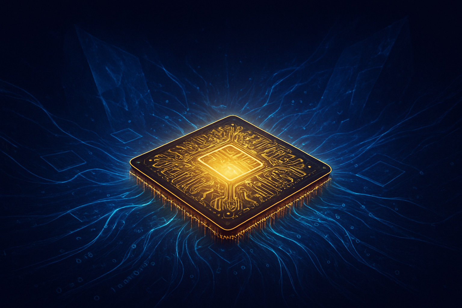
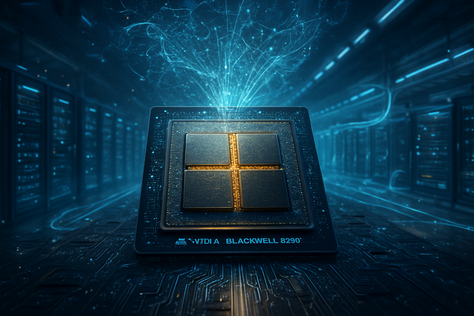
The technical and policy centerpiece of early 2026 is the US Department of Commerce’s "reversal-for-revenue" strategy. In a surprising late-2025 policy shift, the US administration granted NVIDIA Corporation (NASDAQ: NVDA) permission to resume shipments of its high-performance H200 AI chips to select customers in China. However, this comes with a historic caveat: a mandatory 25% "geopolitical risk tax" on every unit sold, paid directly to the US Treasury. This model attempts to balance the commercial needs of American tech giants with the national security goal of funding domestic infrastructure through the profits of competitors.
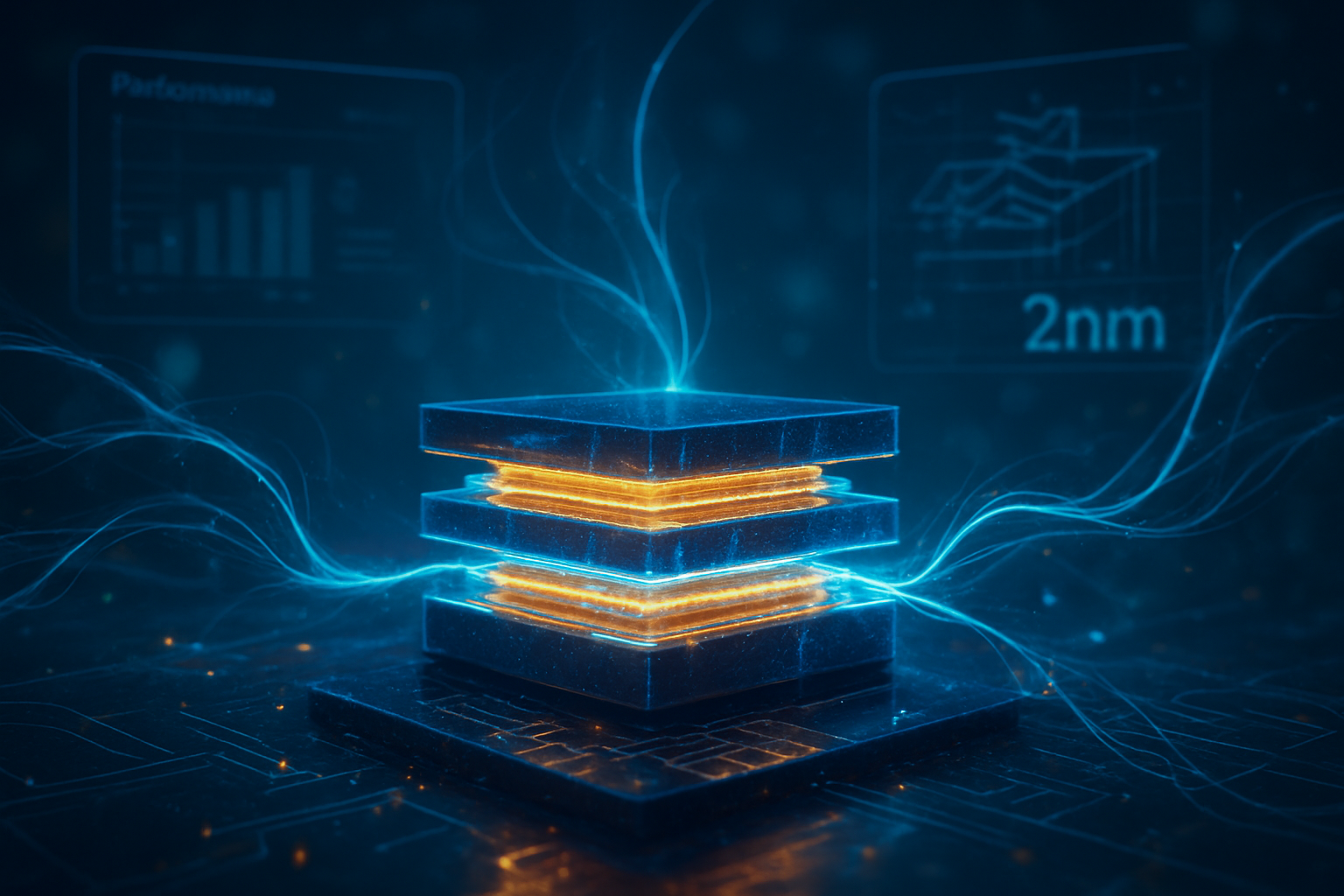
Technologically, the industry has reached the 2-nanometer (2nm) milestone. Taiwan Semiconductor Manufacturing Company (NYSE: TSM) reported this week that its N2 process has achieved commercial yields of nearly 70%, significantly ahead of internal projections. This leap allows for a 15% increase in speed or a 30% reduction in power consumption compared to the previous 3nm generation. This advancement is critical as the "Intelligence Economy" demands more efficient hardware to sustain the massive energy requirements of generative AI models that have now moved from text and image generation into real-time, high-fidelity world simulation.
Initial reactions from the AI research community have been mixed. While the availability of H200-class hardware in China provides a temporary relief valve for global supply chains, industry experts note that the 25% tax effectively creates a "compute divide." Researchers in the West are already eyeing the next generation of Blackwell-Ultra and Rubin architectures, while Chinese firms are being forced to choose between heavily taxed US silicon or domestic alternatives like Huawei’s Ascend series, which Beijing is now mandating for state-level projects.
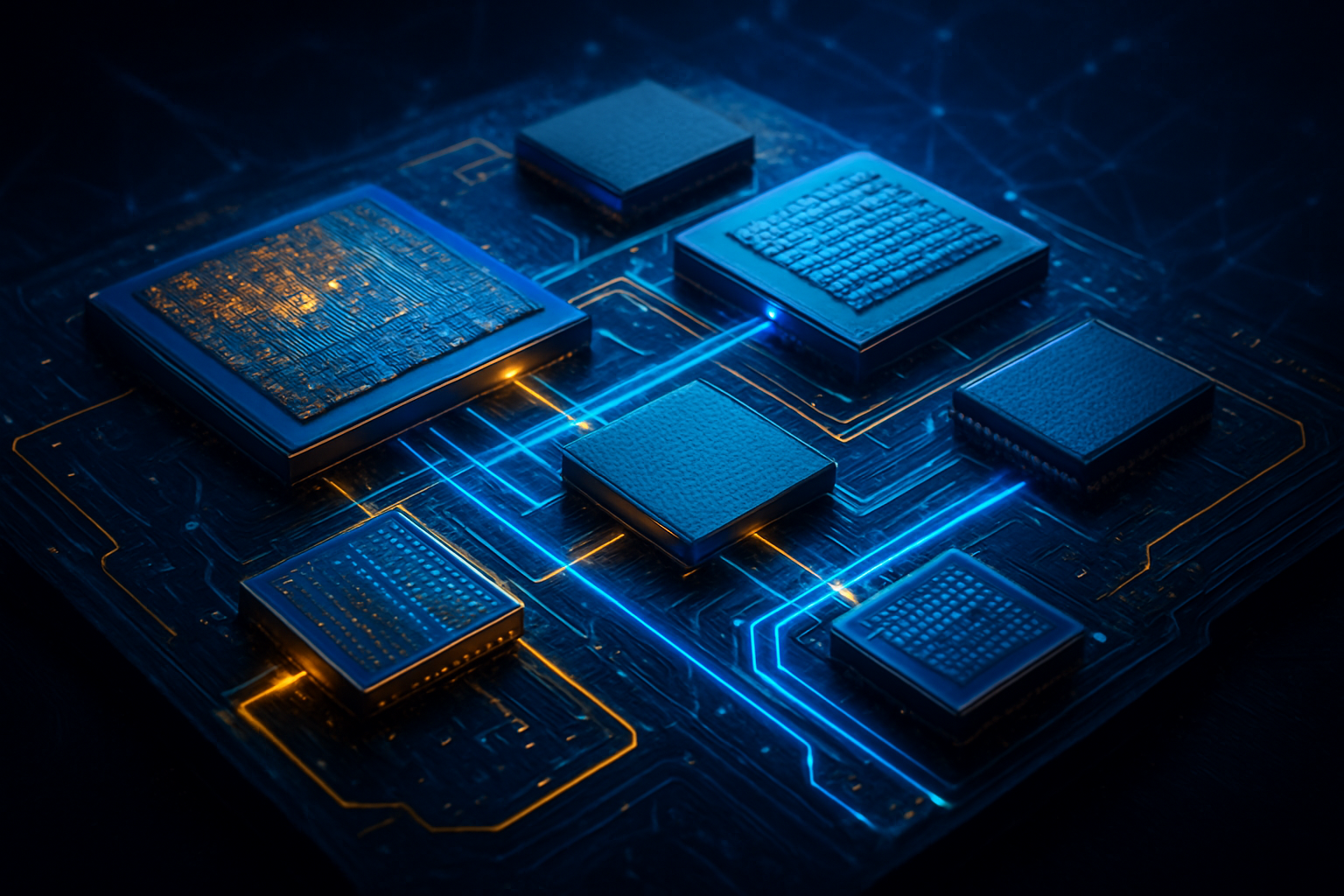
Corporate Giants and the Rise of 'Sovereign AI'
The corporate impact of these shifts is most visible in the partial "nationalization" of Intel Corporation (NASDAQ: INTC). Following a period of financial volatility in late 2025, the US government intervened with an $8.9 billion stock purchase, funded by the Secure Enclave program. This move ensures that the Department of Defense has a guaranteed, domestic source for leading-edge military and intelligence chips. Intel is now effectively a public-private partnership, focused on its Arizona and Oregon "Secure Enclaves" to maintain a "frontier compute" lead over global rivals.
NVIDIA, meanwhile, is navigating a complex dual-market strategy. While facing a soft boycott in China—where Beijing has directed local firms to halt H200 orders in favor of domestic chips—the company has found a massive new growth engine in the Middle East. In late December 2025, the US greenlit a $1 billion shipment of 35,000 advanced chips to Saudi Arabia’s HUMAIN project and the UAE’s G42. This deal was contingent on the total removal of Chinese hardware from those nations' data centers, illustrating how the US is using its "silicon hegemony" to forge new diplomatic and technological alliances.
Other major players like Advanced Micro Devices, Inc. (NASDAQ: AMD) and ASML Holding N.V. (NASDAQ: ASML) are adjusting to this highly regulated environment. AMD has seen increased demand for its MI350 series in markets where NVIDIA’s tax-heavy H200s are less competitive, while ASML continues to face tightening restrictions on the export of its High-NA EUV lithography machines, further cementing the "technological moat" around the US and its immediate allies.
Geopolitical Friction and the 'Third Path'
The wider significance of these developments lies in the aggressive stance the US is taking against even minor "on-ramps" for foreign influence. On January 2, 2026, a Presidential Executive Order blocked the $3 million acquisition of assets from Emcore Corporation (NASDAQ: EMKR) by HieFo Corp, a firm identified as having ties to Chinese nationals. While the deal was small in dollar terms, the focus was on Emcore’s expertise in indium phosphide (InP) chips—a technology vital for military lasers and advanced sensors. This underscores a policy of "zero-leakage" for dual-use technologies.
In Europe, a "Third Path" is emerging. All 27 EU member states recently signed a declaration calling for "EU Chips Act 2.0," with a formal review scheduled for the first quarter of 2026. The goal is to secure €20 billion in additional funding to help Europe reach a 20% global market share by 2030. The EU is positioning itself as the global leader in specialized "specialty" chips for the automotive and industrial sectors, attempting to remain a neutral ground while the US and China continue their high-stakes compute race.
This landscape is a stark departure from the early 2020s. We are no longer seeing a "chip shortage" driven by supply chain hiccups, but a "compute containment" strategy. The US is leveraging its 8:1 advantage in frontier compute capacity to dictate the terms of the global AI rollout, while China counters by leveraging its dominance in the critical mineral supply chains—gallium, germanium, and rare earths—necessary to build the next generation of hardware.
The Road to 2030: Challenges and Predictions
Looking ahead, the next 12 to 24 months will likely see the formalization of "CHIPS 2.0" in the United States. Rather than just building factories, the focus is shifting toward fraud risk management and the oversight of the original $50 billion fund. Experts predict that by 2027, the US will attempt to create a "Silicon NATO"—a formal alliance of nations that share compute resources and research while maintaining a unified export front against non-aligned states.
A major challenge remains the "Malaysia Shift." Companies like Nexperia, currently under pressure due to Chinese ownership, are rapidly moving production to Southeast Asia to avoid "penetrating sanctions." This migration is creating a new semiconductor hub in Malaysia and Vietnam, which could eventually challenge the established order if they can move up the value chain from assembly and testing to actual wafer fabrication.
Predicting the next move, analysts suggest that the "Intelligence Economy" will drive the semiconductor market toward $1.5 trillion by 2030. The primary hurdle will not be the physics of the chips themselves, but the geopolitical friction of their distribution. As AI models become more integrated into national infrastructure, the "sovereignty" of the silicon they run on will become the most important metric for any nation's security.
Summary of the New Silicon Order
The events of early 2026 mark a definitive turning point in the history of technology. The transition from free-market competition to "managed bifurcation" reflects the reality that semiconductors are now the foundational resource of the 21st century. The US government’s active role—from taking stakes in Intel to taxing NVIDIA’s exports—shows that the "invisible hand" of the market has been replaced by the strategic hand of the state.
Key takeaways for the coming weeks include the EU’s formal decision on Chips Act 2.0 funding and the potential for a Chinese counter-response regarding critical mineral exports. As we monitor these developments, the central question remains: can the world sustain a $1 trillion industry that is increasingly divided by digital iron curtains, or will the cost of bifurcation eventually stifle the very AI revolution it seeks to control?
This content is intended for informational purposes only and represents analysis of current AI developments.
TokenRing AI delivers enterprise-grade solutions for multi-agent AI workflow orchestration, AI-powered development tools, and seamless remote collaboration platforms.
For more information, visit https://www.tokenring.ai/.