As of early 2026, the semiconductor industry has reached a pivotal inflection point in the race to sustain the generative AI revolution. The traditional organic materials that have housed microchips for decades have officially hit a "warpage wall," threatening to stall the development of increasingly massive AI accelerators. In response, a high-stakes transition to glass substrates has moved from experimental laboratories to the forefront of commercial manufacturing, marking the most significant shift in chip packaging technology in over twenty years.
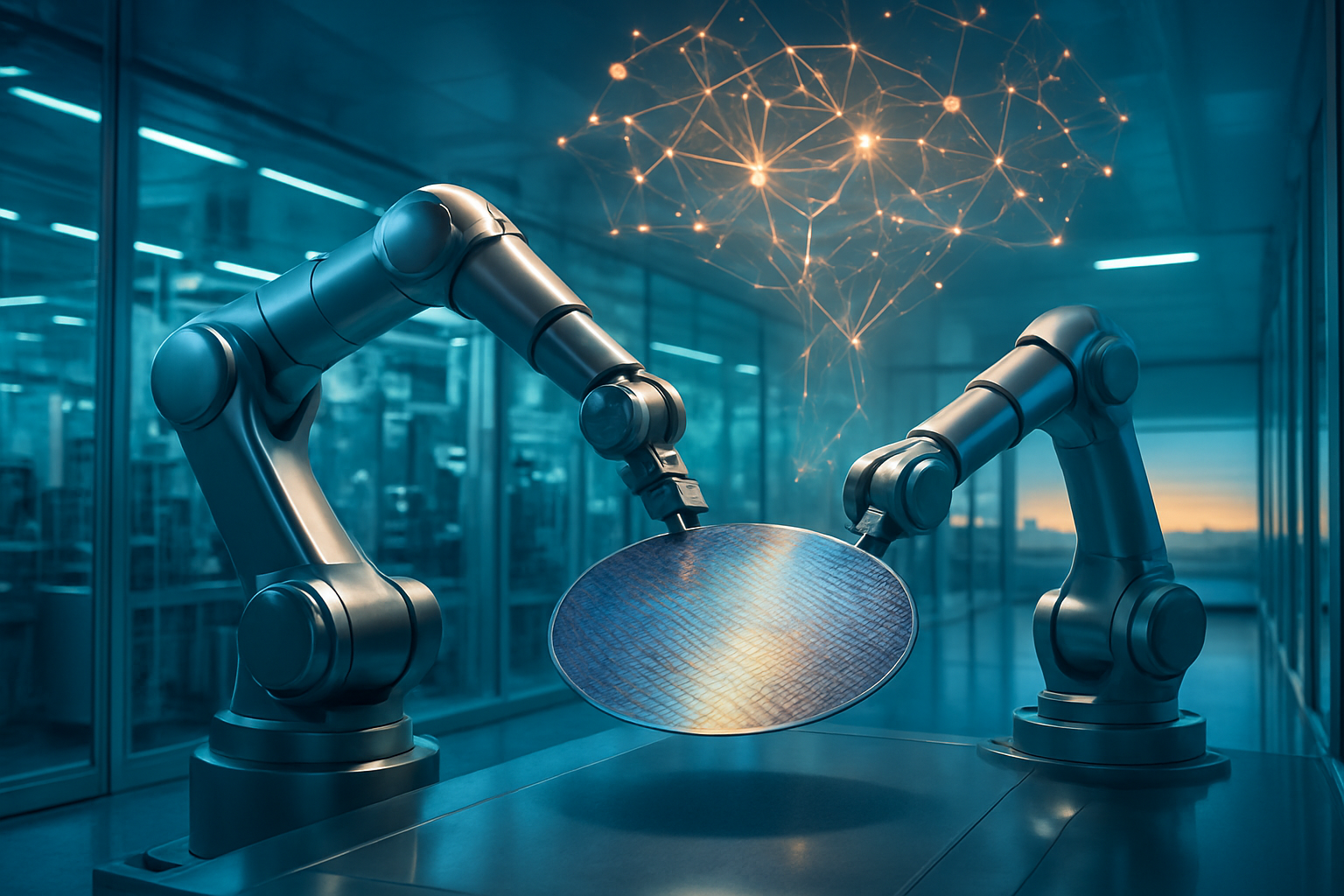
This migration is not merely an incremental upgrade; it is a fundamental re-engineering of how silicon interacts with the physical world. By replacing organic resin with ultra-thin, high-strength glass, industry titans are enabling a 10x increase in interconnect density, allowing for the creation of "super-chips" that were previously impossible to manufacture. With Intel (NASDAQ: INTC), Samsung (KRX: 005930), and TSMC (NYSE: TSM) all racing to deploy glass-based solutions by 2026 and 2027, the battle for AI dominance has moved from the transistor level to the very foundation of the package.
The Technical Breakthrough: Overcoming the Warpage Wall
For years, the industry relied on Ajinomoto Build-up Film (ABF), an organic resin, to create the substrates that connect chips to circuit boards. however, as AI accelerators like those from NVIDIA (NASDAQ: NVDA) and AMD (NASDAQ: AMD) have grown larger and more power-hungry—often exceeding 1,000 watts of thermal design power—ABF has reached its physical limit. The primary culprit is the "warpage wall," a phenomenon caused by the mismatch in the Coefficient of Thermal Expansion (CTE) between silicon and organic materials. As these massive chips heat up and cool down, the organic substrate expands and contracts at a different rate than the silicon, causing the entire package to warp. This warping leads to cracked connections and "micro-bump" failures, effectively capping the size and complexity of next-generation AI hardware.
Glass substrates solve this dilemma by offering a CTE that nearly matches silicon, providing unparalleled dimensional stability even at temperatures reaching 500°C. Beyond structural integrity, glass enables a massive leap in interconnect density through the use of Through-Glass Vias (TGVs). Unlike organic substrates, which require mechanical drilling that limits how closely connections can be spaced, glass can be etched with high-precision lasers. This allows for an interconnect pitch of less than 10 micrometers—a 10x improvement over the 100-micrometer pitch common in organic materials. This density is critical for the ultra-high-bandwidth memory (HBM4) and multi-die architectures required to train the next generation of Large Language Models (LLMs).
Furthermore, glass provides superior electrical properties, reducing signal loss by up to 40% and cutting the power required for data movement by half. In an era where data center energy consumption is a global concern, the efficiency gains of glass are as valuable as its performance metrics. Initial reactions from the research community have been overwhelmingly positive, with experts noting that glass allows the industry to treat the entire package as a single, massive "system-on-wafer," effectively extending the life of Moore's Law through advanced packaging rather than just transistor scaling.
The Corporate Race: Intel, Samsung, and the Triple Alliance
The competition to bring glass substrates to market has ignited a fierce rivalry between the world’s leading foundries. Intel has taken an early lead, leveraging over a decade of research to establish a $1 billion commercial-grade pilot line in Chandler, Arizona. As of January 2026, Intel’s Chandler facility is actively producing glass cores for high-volume customers. This head start has allowed Intel Foundry to position glass packaging as a flagship differentiator, attracting cloud service providers who are designing custom AI silicon and need the thermal resilience that only glass can provide.
Samsung has responded by forming a "Triple Alliance" that spans its most powerful divisions: Samsung Electronics, Samsung Display, and Samsung Electro-Mechanics. By repurposing the glass-processing expertise from its world-leading OLED and LCD businesses, Samsung has bypassed many of the supply chain hurdles that have slowed others. At the start of 2026, Samsung’s Sejong pilot line completed its final verification phase, with the company announcing at CES 2026 that it is on track for full-scale mass production by the end of the year. This integrated approach allows Samsung to offer an end-to-end glass solution, from the raw glass core to the final integrated AI package.
Meanwhile, TSMC has pivoted toward a "rectangular revolution" known as Fan-Out Panel-Level Packaging (FO-PLP) on glass. By moving from traditional circular wafers to 600mm x 600mm rectangular glass panels, TSMC aims to increase area utilization from roughly 57% to over 80%, significantly lowering the cost of large-scale AI chips. TSMC’s branding for this effort, CoPoS (Chip-on-Panel-on-Substrate), is expected to be the successor to its industry-standard CoWoS technology. While TSMC is currently stabilizing yields on smaller 300mm panels at its Chiayi facility, the company is widely expected to ramp to full panel-level production by 2027, ensuring it remains the primary manufacturer for high-volume players like NVIDIA.
Broader Significance: The Package is the New Transistor
The shift to glass substrates represents a fundamental change in the AI landscape, signaling that the "package" has become as important as the "chip" itself. For the past decade, AI performance gains were largely driven by making transistors smaller. However, as we approach the physical limits of atomic-scale manufacturing, the bottleneck has shifted to how those transistors communicate and stay cool. Glass substrates remove this bottleneck, enabling the creation of 1-trillion-transistor packages that can span the size of an entire palm, a feat that would have been physically impossible with organic materials.
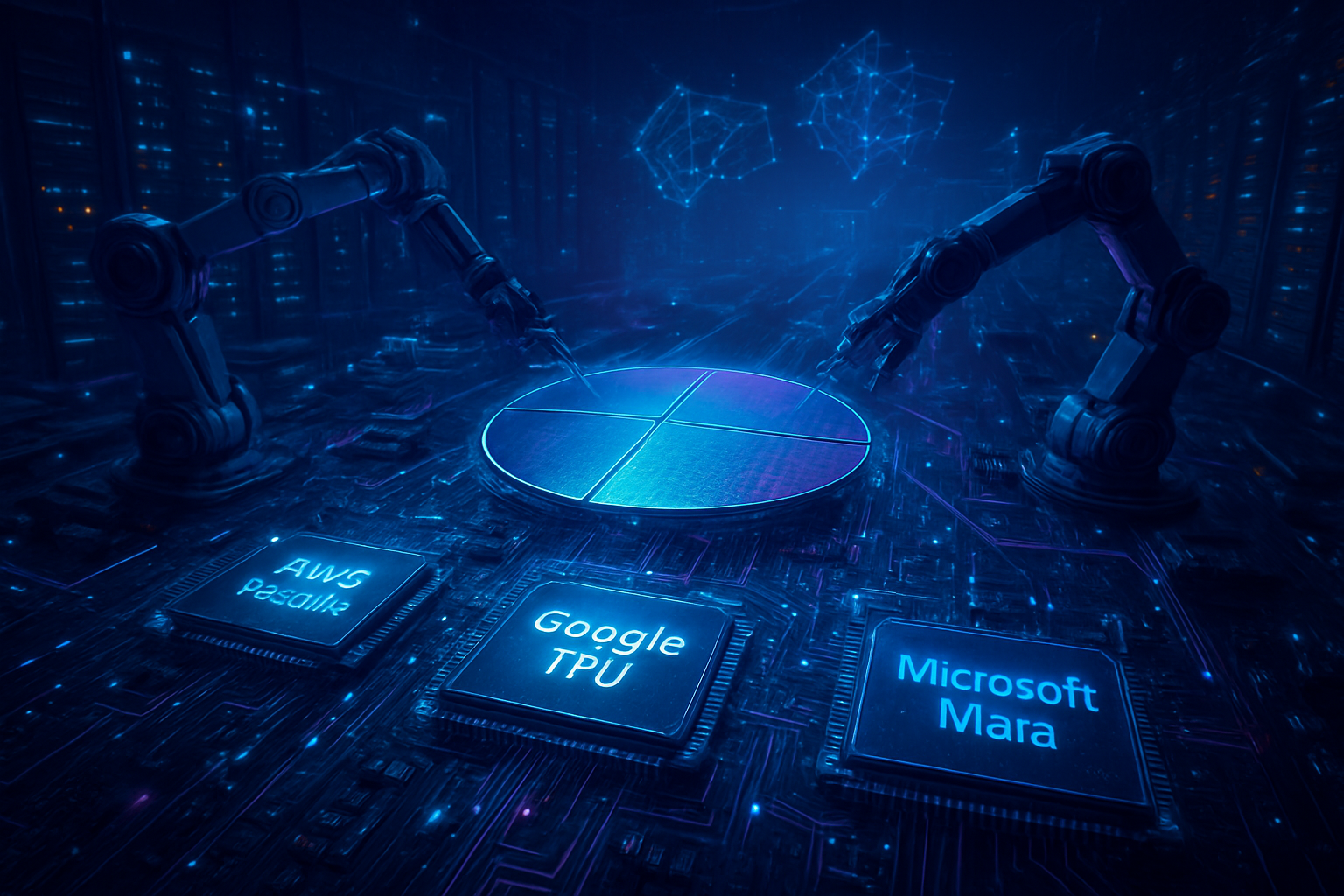
This development also has profound implications for the geography of semiconductor manufacturing. Intel’s investment in Arizona and the emergence of Absolics (a subsidiary of SKC) in Georgia, USA, suggest that advanced packaging could become a cornerstone of the "onshoring" movement. By bringing high-end glass substrate production to the United States, these companies are shortening the supply chain for American AI giants like Microsoft (NASDAQ: MSFT) and Google (NASDAQ: GOOGL), who are increasingly reliant on custom-designed accelerators to run their massive AI workloads.
However, the transition is not without its challenges. The fragility of glass during the manufacturing process remains a concern, requiring entirely new handling equipment and cleanroom protocols. Critics also point to the high initial cost of glass substrates, which may limit their use to the most expensive AI and high-performance computing (HPC) chips for the next several years. Despite these hurdles, the industry consensus is clear: without glass, the thermal and physical scaling of AI hardware would have hit a dead end.
Future Horizons: Toward Optical Interconnects and 2027 Scaling
Looking ahead, the roadmap for glass substrates extends far beyond simple structural support. By 2027, the industry expects to see the first wave of "Second Generation" glass packages that integrate silicon photonics directly into the substrate. Because glass is transparent, it allows for the seamless integration of optical interconnects, enabling chips to communicate using light rather than electricity. This would theoretically provide another order-of-magnitude jump in data transfer speeds while further reducing power consumption, a holy grail for the next decade of AI development.
AMD is already in advanced evaluation phases for its MI400 series accelerators, which are rumored to be among the first to fully utilize these glass-integrated optical paths. As the technology matures, we can expect to see glass substrates trickle down from high-end data centers into high-performance consumer electronics, such as workstations for AI researchers and creators. The long-term vision is a modular "chiplet" ecosystem where different components from different manufacturers can be tiled onto a single glass substrate with near-zero latency between them.
The primary challenge moving forward will be achieving the yields necessary for true mass-market adoption. While pilot lines are operational in early 2026, scaling to millions of units per month will require a robust global supply chain for high-purity glass and specialized laser-drilling equipment. Experts predict that 2026 will be the "year of the pilot," with 2027 serving as the true breakout year for glass-core AI hardware.
A New Era for AI Infrastructure
The industry-wide shift to glass substrates marks the end of the organic era for high-performance computing. By shattering the warpage wall and enabling a 10x leap in interconnect density, glass has provided the physical foundation necessary for the next decade of AI breakthroughs. Whether it is Intel's first-mover advantage in Arizona, Samsung's triple-division alliance, or TSMC's rectangular panel efficiency, the leaders of the semiconductor world have all placed their bets on glass.
As we move through 2026, the success of these pilot lines will determine which companies lead the next phase of the AI gold rush. For investors and tech enthusiasts, the key metrics to watch will be the yield rates of these new facilities and the performance benchmarks of the first glass-backed AI accelerators hitting the market in the second half of the year. The transition to glass is more than a material change; it is the moment the semiconductor industry stopped building bigger chips and started building better systems.
This content is intended for informational purposes only and represents analysis of current AI developments.
TokenRing AI delivers enterprise-grade solutions for multi-agent AI workflow orchestration, AI-powered development tools, and seamless remote collaboration platforms.
For more information, visit https://www.tokenring.ai/.