The global landscape of artificial intelligence hardware underwent a seismic shift on January 2, 2026, as Shanghai Biren Technology Co. Ltd. (HKG: 06082) made its historic debut on the Hong Kong Stock Exchange. In a stunning display of investor confidence and geopolitical defiance, Biren’s shares surged by 76.2% on their first day of trading, closing at HK$34.46 after an intraday peak that saw the stock more than double its initial offering price of HK$19.60. The IPO, which raised approximately HK$5.58 billion (US$717 million), was oversubscribed by a staggering 2,348 times in the retail tranche, signaling a massive "chip frenzy" as China accelerates its pursuit of semiconductor self-sufficiency.
This explosive market entry represents more than just a successful financial exit for Biren’s early backers; it marks the emergence of a viable domestic alternative to Western silicon. As U.S. export controls continue to restrict the flow of high-end chips from NVIDIA (NASDAQ: NVDA) and AMD (NASDAQ: AMD) into the Chinese market, Biren has positioned itself as the primary beneficiary of a trillion-dollar domestic AI vacuum. The success of the IPO underscores a growing consensus among global investors: the era of Western chip hegemony is facing its most significant challenge yet from a new generation of Chinese "unicorns" that are learning to innovate under the pressure of sanctions.
The Technical Edge: Bridging the Gap with Chiplets and BIRENSUPA
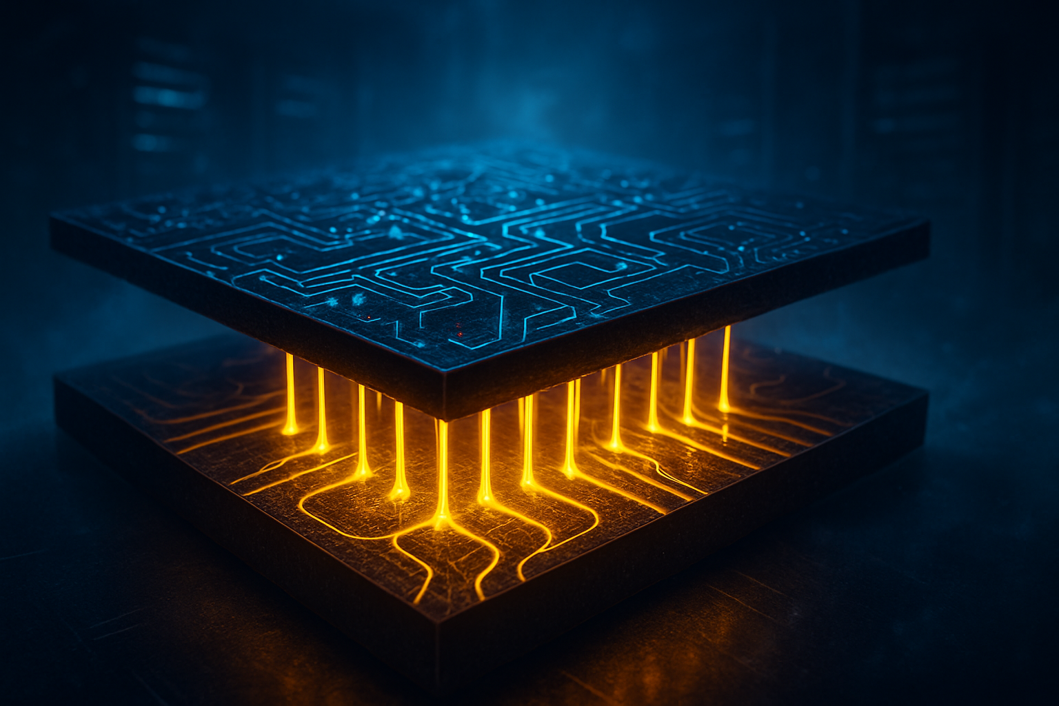
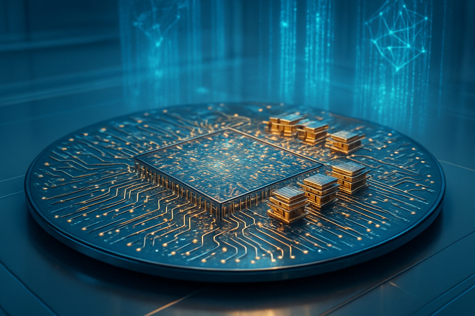
At the heart of Biren’s market appeal is its flagship BR100 series, a general-purpose graphics processing unit (GPGPU) designed specifically for large-scale AI training and high-performance computing (HPC). Built on the proprietary "BiLiren" architecture, the BR100 utilizes a sophisticated 7nm process technology. While this trails the 4nm nodes used by NVIDIA’s latest Blackwell architecture, Biren has employed a clever "chiplet" design to overcome manufacturing limitations. By splitting the processor into multiple smaller tiles and utilizing advanced 2.5D CoWoS packaging, Biren has improved manufacturing yields by roughly 20%, a critical innovation given the restricted access to the world’s most advanced lithography equipment.
Technically, the BR100 is no lightweight. It delivers up to 2,048 TFLOPs of compute power in BF16 precision and features 77 billion transistors. To address the "memory wall"—the bottleneck where data processing speeds outpace data delivery—the chip integrates 64GB of HBM2e memory with a bandwidth of 2.3 TB/s. While these specs place it roughly on par with NVIDIA’s A100 in raw power, Biren’s hardware has demonstrated 2.6x speedups over the A100 in specific domestic benchmarks for natural language processing (NLP) and computer vision, proving that software-hardware co-design can compensate for older process nodes.
Initial reactions from the AI research community have been cautiously optimistic. Experts note that Biren’s greatest achievement isn't just the hardware, but its "BIRENSUPA" software platform. For years, NVIDIA’s "CUDA moat"—a proprietary software ecosystem that makes it difficult for developers to switch hardware—has been the primary barrier to entry for competitors. BIRENSUPA aims to bypass this by offering seamless integration with mainstream frameworks like PyTorch and Baidu’s (NASDAQ: BIDU) PaddlePaddle. By focusing on a "plug-and-play" experience for Chinese developers, Biren is lowering the switching costs that have historically kept NVIDIA entrenched in Chinese data centers.
A New Competitive Order: The "Good Enough" Strategy
The surge in Biren’s valuation has immediate implications for the global AI hierarchy. While NVIDIA and AMD remain the gold standard for cutting-edge frontier models in the West, Biren is successfully executing a "good enough" strategy in the East. By providing hardware that is "comparable" to previous-generation Western chips but available without the risk of sudden U.S. regulatory bans, Biren has secured massive procurement contracts from state-owned enterprises, including China Mobile (HKG: 0941) and China Telecom (HKG: 0728). This guaranteed domestic demand provides a stable revenue floor that Western firms can no longer count on in the region.
For major Chinese tech giants like Alibaba (NYSE: BABA) and Tencent (HKG: 0700), Biren represents a critical insurance policy. As these companies race to build their own proprietary Large Language Models (LLMs) to compete with OpenAI and Google, the ability to source tens of thousands of GPUs domestically is a matter of national and corporate security. Biren’s IPO success suggests that the market now views domestic chipmakers not as experimental startups, but as essential infrastructure providers. This shift threatens to permanently erode NVIDIA’s market share in what was once its second-largest territory, potentially costing the Santa Clara giant billions in long-term revenue.
Furthermore, the capital infusion from the IPO allows Biren to aggressively poach talent and expand its R&D. The company has already announced that 85% of the proceeds will be directed toward the development of the BR200 series, which is expected to integrate HBM3e memory. This move directly targets the high-bandwidth requirements of 2026-era models like DeepSeek-V3 and Llama 4. By narrowing the hardware gap, Biren is forcing Western companies to innovate faster while simultaneously fighting a price war in the Asian market.
Geopolitics and the Great Decoupling
The broader significance of Biren’s explosive IPO cannot be overstated. It is a vivid illustration of the "Great Decoupling" in the global technology sector. Since being added to the U.S. Entity List in October 2023, Biren has been forced to navigate a minefield of export controls. Instead of collapsing, the company has pivoted, relying on domestic foundry SMIC (HKG: 0981) and local high-bandwidth memory (HBM) alternatives. This resilience has turned Biren into a symbol of Chinese technological nationalism, attracting "patriotic capital" that is less concerned with immediate dividends and more focused on long-term strategic sovereignty.
This development also highlights the limitations of export controls as a long-term strategy. While U.S. sanctions successfully slowed China’s progress at the 3nm and 2nm nodes, they have inadvertently created a protected incubator for domestic firms. Without competition from NVIDIA’s latest H100 or Blackwell chips, Biren has had the "room to breathe," allowing it to iterate on its architecture and build a loyal customer base. The 76% surge in its IPO price reflects a market bet that China will successfully build a parallel AI ecosystem—one that is entirely independent of the U.S. supply chain.
However, potential concerns remain. The bifurcation of the AI hardware market could lead to a fragmented software landscape, where models trained on Biren hardware are not easily portable to NVIDIA systems. This could slow global AI collaboration and lead to "AI silos." Moreover, Biren’s reliance on older manufacturing nodes means its chips are inherently less energy-efficient than their Western counterparts, a significant drawback as the world grapples with the massive power demands of AI data centers.
The Road Ahead: HBM3e and the BR200 Series
Looking toward the near-term future, the industry is closely watching the transition to the BR200 series. Expected to launch in late 2026, this next generation of silicon will be the true test of Biren’s ability to compete on the global stage. The integration of HBM3e memory is a high-stakes gamble; if Biren can successfully mass-produce these chips using domestic packaging techniques, it will have effectively neutralized the most potent parts of the current U.S. trade restrictions.
Experts predict that the next phase of competition will move beyond raw compute power and into the realm of "edge AI" and specialized inference chips. Biren is already rumored to be working on a series of low-power chips designed for autonomous vehicles and industrial robotics—sectors where China already holds a dominant manufacturing position. If Biren can become the "brains" of China’s massive EV and robotics industries, its current IPO valuation might actually look conservative in retrospect.
The primary challenge remains the supply chain. While SMIC has made strides in 7nm production, scaling to the volumes required for a global AI revolution remains a hurdle. Biren must also continue to evolve its software stack to keep pace with the rapidly changing world of transformer architectures and agentic AI. The coming months will be a period of intense scaling for Biren as it attempts to move from a "national champion" to a global contender.
A Watershed Moment for AI Hardware
Biren Technology’s 76% IPO surge is a landmark event in the history of artificial intelligence. It signals that the "chip war" has entered a new, more mature phase—one where Chinese firms are no longer just trying to survive, but are actively thriving and attracting massive amounts of public capital. The success of this listing provides a blueprint for other Chinese semiconductor firms, such as Moore Threads and Enflame, to seek public markets and fuel their own growth.
The key takeaway is that the AI hardware market is no longer a one-horse race. While NVIDIA (NASDAQ: NVDA) remains the technological leader, Biren’s emergence proves that a "second ecosystem" is not just possible—it is already here. This development will likely lead to more aggressive price competition, a faster pace of innovation, and a continued shift in the global balance of technological power.
In the coming weeks and months, investors and policy-makers will be watching Biren’s production ramp-up and the performance of the BR100 in real-world data center deployments. If Biren can deliver on its technical promises and maintain its stock momentum, January 2, 2026, will be remembered as the day the global AI hardware market officially became multipolar.
This content is intended for informational purposes only and represents analysis of current AI developments.
TokenRing AI delivers enterprise-grade solutions for multi-agent AI workflow orchestration, AI-powered development tools, and seamless remote collaboration platforms.
For more information, visit https://www.tokenring.ai/.