Tag: AI Hardware

  • Intel’s Angstrom Era Arrives: 18A and 14A Multi-Chiplet Breakthroughs Signal a New Frontier in AI Compute

    Intel’s Angstrom Era Arrives: 18A and 14A Multi-Chiplet Breakthroughs Signal a New Frontier in AI Compute

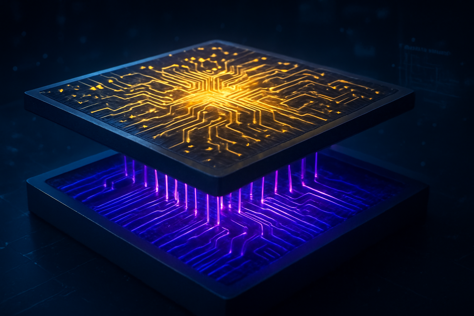
    In a landmark demonstration of semiconductor engineering, Intel (NASDAQ: INTC) has officially showcased its next-generation multi-chiplet processors built on the 18A and 14A process nodes. This milestone, revealed at the start of 2026, marks the successful culmination of Intel’s "five nodes in four years" strategy and signals the company's aggressive return to the forefront of the silicon manufacturing race. By leveraging advanced 3D packaging and the industry’s first commercial implementation of High-Numerical Aperture (High-NA) EUV lithography, Intel is positioning itself as a formidable "Systems Foundry" capable of producing the massive, high-density chips required for the next decade of artificial intelligence and high-performance computing (HPC).

    The showcase featured the first live silicon of the "Clearwater Forest" Xeon processor, a multi-tile marvel that utilizes Intel 18A for its compute logic, and a conceptual "Mega-Package" built on the upcoming 14A node. These developments are not merely incremental updates; they represent a fundamental shift in how chips are designed and manufactured. By decoupling the various components of a processor into specialized "chiplets" and reassembling them with high-speed interconnects, Intel is challenging the dominance of Taiwan Semiconductor Manufacturing Company (NYSE: TSM) and aiming to reclaim the crown of process leadership it lost nearly a decade ago.

    Technical Breakthroughs: RibbonFET, PowerVia, and High-NA EUV

    The technical foundation of Intel’s resurgence lies in two revolutionary technologies: RibbonFET and PowerVia. RibbonFET, Intel’s implementation of a Gate-All-Around (GAA) transistor, is now in high-volume manufacturing on the 18A node. Unlike traditional FinFETs, RibbonFET surrounds the transistor channel on all four sides, allowing for precise control over current flow and significantly reducing power leakage—a critical requirement for AI data centers operating at the edge of thermal limits. Complementing this is PowerVia, a groundbreaking "backside power delivery" system that moves power routing to the reverse side of the silicon wafer. This separation of power and signal lines eliminates the "wiring congestion" that has plagued chip designers for years, enabling higher clock speeds and improved energy efficiency.

    Moving beyond 18A, the 14A node represents Intel's first full-scale utilization of High-NA EUV lithography, powered by the ASML (NASDAQ: ASML) Twinscan EXE:5200B. This advanced machinery provides a resolution of 8nm, nearly doubling the precision of standard EUV tools. For the 14A node, this allows Intel to print the most critical circuit patterns in a single pass, avoiding the complexity and yield-loss risks associated with multi-patterning. Furthermore, Intel has introduced "PowerDirect" on the 14A node, a second-generation backside power solution designed to handle the extreme current densities required by future AI accelerators.

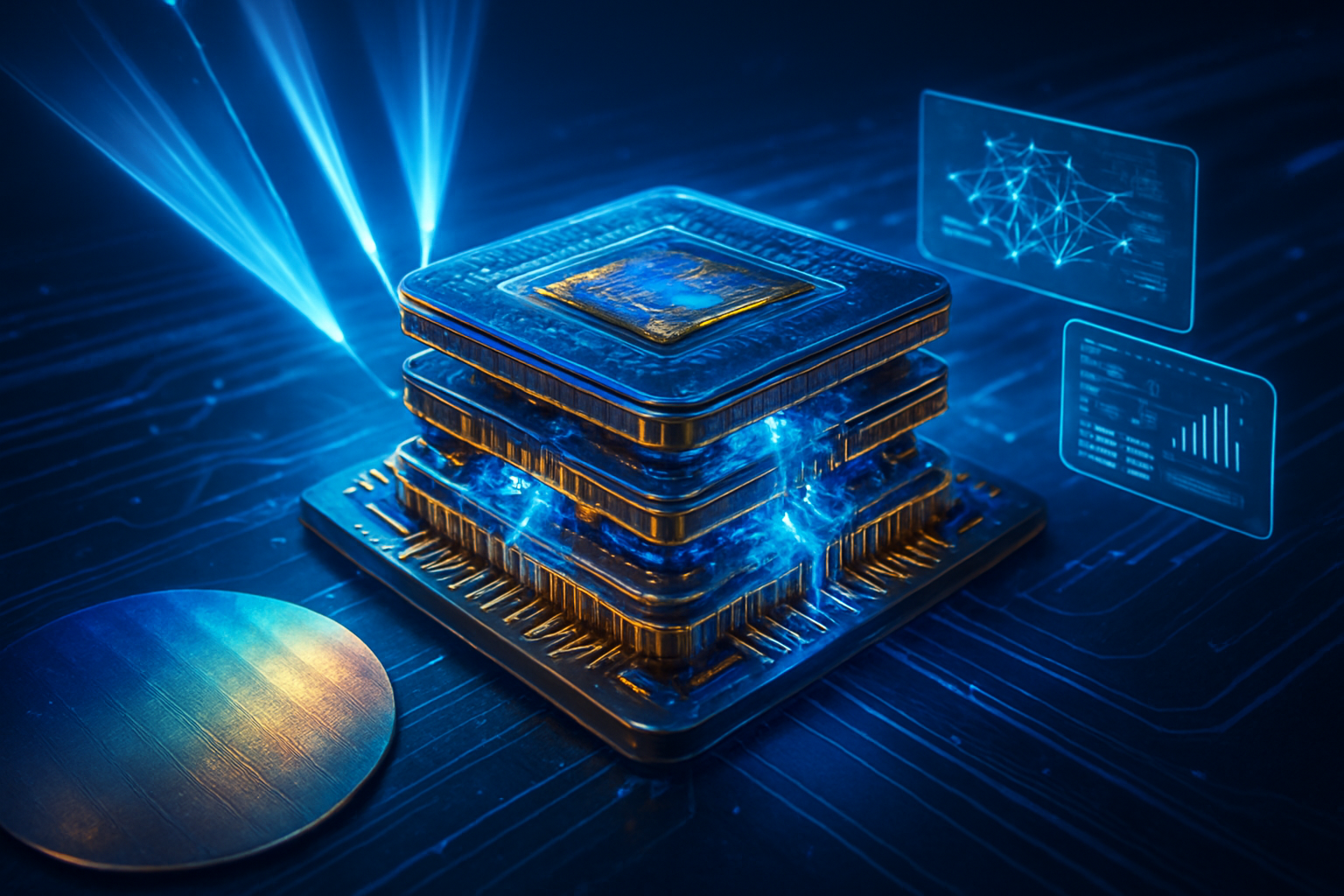
    The multi-chiplet architecture showcased by Intel also highlights the company’s lead in advanced packaging. Using Foveros Direct 3D and EMIB (Embedded Multi-die Interconnect Bridge), Intel demonstrated the ability to stack and tile chips with unprecedented density. One of the most striking reveals was a 14A-based AI "Mega-Package" that integrates 16 compute tiles with 24 stacks of HBM5 memory. To manage the immense heat and physical stress of such a large package, Intel has transitioned to glass substrates, which offer 50% less pattern distortion and superior thermal stability compared to traditional organic materials.

    Initial reactions from the semiconductor research community have been cautiously optimistic, with many experts noting that Intel has achieved a significant "first-mover" advantage in backside power delivery. While TSMC and Samsung (KRX: 005930) are working on similar technologies, Intel’s 18A is the first to reach high-volume production with these features. Industry analysts suggest that if Intel can maintain its yield rates, the combination of RibbonFET, PowerVia, and High-NA EUV could provide a 12-to-18-month technological lead over its rivals in specific high-performance metrics.

    Market Impact: Securing the AI Supply Chain

    The implications for the broader tech industry are profound, as Intel Foundry begins to secure "anchor" customers who were previously reliant solely on TSMC. Microsoft (NASDAQ: MSFT) has already committed to using the 18A and 18A-P nodes for its next-generation Maia 2 AI accelerators, a move that allows the software giant to secure a domestic U.S. supply chain for its Azure AI infrastructure. Similarly, Amazon (NASDAQ: AMZN) through its AWS division, has signed a multi-billion dollar deal to produce custom Trainium3 chips on Intel’s 18A node. These partnerships validate Intel’s "Systems Foundry" model, where the company provides not just the silicon, but the packaging and interconnect standards necessary for complex AI systems.

    NVIDIA (NASDAQ: NVDA), the current king of AI hardware, has also entered the fold in a strategic shift that could disrupt the status quo. While NVIDIA continues to manufacture its primary GPUs with TSMC, it has signed a landmark $5 billion agreement to utilize Intel’s advanced packaging services. More intriguingly, the two companies are reportedly co-developing "Intel x86 RTX SOCs"—hybrid processors that fuse Intel’s high-performance x86 cores with NVIDIA’s RTX graphics chiplets. This collaboration suggests that even the fiercest competitors see the value in Intel’s unique packaging capabilities, potentially leading to a new class of "best-of-both-worlds" hardware for workstations and high-end gaming.

    For startups and smaller AI labs, Intel’s progress offers a much-needed alternative in a market that has been bottlenecked by TSMC’s capacity limits. By providing a credible second source for leading-edge manufacturing, Intel is likely to drive down costs and accelerate the pace of hardware iteration. However, the competitive pressure on TSMC remains high; the Taiwanese giant still holds the lead in raw transistor density and has a decades-long track record of manufacturing reliability. Intel’s challenge will be to prove that it can match TSMC’s legendary yield consistency at scale, especially as it navigates the transition to the 14A node.

    Geopolitics and the New "System-Level" Moore’s Law

    Beyond the corporate rivalry, Intel’s 18A and 14A progress carries significant geopolitical and economic weight. As the only Western company capable of manufacturing chips at the Angstrom level, Intel is the primary beneficiary of the U.S. CHIPS and Science Act. The successful ramp-up of Fab 52 in Arizona and the High-NA installation in Oregon are seen as critical milestones in the effort to rebalance the global semiconductor supply chain, which is currently heavily concentrated in East Asia. This "Silicon Shield" strategy is designed to ensure that the most advanced AI capabilities remain accessible to Western nations regardless of regional instability.

    The shift toward multi-chiplet "systems-on-package" also signals the end of the traditional Moore’s Law era, where performance gains were driven primarily by shrinking individual transistors. We are now entering the era of "System-Level Moore’s Law," where the focus has shifted to how efficiently different chips can talk to one another. Intel’s embrace of open standards like UCIe (Universal Chiplet Interconnect Express) ensures that its 18A and 14A nodes can serve as a "chassis" for a diverse ecosystem of chiplets from different vendors, fostering a more modular and innovative hardware landscape.

    However, this transition is not without its concerns. The extreme cost of High-NA EUV tools—upwards of $350 million per machine—and the complexity of glass substrate manufacturing create a high barrier to entry that could further centralize power among a few "mega-foundries." There are also environmental considerations; the massive energy requirements of these advanced fabs and the AI chips they produce continue to be a point of contention for sustainability advocates. Despite these challenges, the leap from the 5nm/3nm era to the 1.8nm/1.4nm era is being hailed as the most significant jump in computing power since the introduction of the microprocessor.

    The Road to 10A: What’s Next for Intel Foundry?

    Looking ahead, the roadmap for 2026 and beyond is focused on the refinement of the 14A node and the early research into the "10A" (1nm) generation. Intel has hinted that its 14A-P (Performance) variant, expected in late 2027, will introduce even more advanced 3D stacking techniques that could allow for memory to be bonded directly on top of logic with near-zero latency. This would be a game-changer for Large Language Models (LLMs) that are currently limited by the "memory wall"—the speed at which data can move between the processor and RAM.

    Experts predict that the next two years will see a surge in "specialized AI silicon" as companies move away from general-purpose GPUs toward custom chiplet-based designs tailored for specific neural network architectures. Intel’s ability to offer a "menu" of chiplets—some on 18A for efficiency, some on 14A for peak performance—will likely make it the preferred partner for this custom silicon wave. The main hurdle remains the software stack; while Intel’s hardware is catching up, it must continue to invest in its OneAPI and OpenVINO platforms to ensure that developers can easily port their AI workloads from NVIDIA’s proprietary CUDA environment.

    Conclusion: A New Chapter in Silicon History

    The showcase of Intel’s 18A and 14A nodes marks a definitive turning point in the history of the semiconductor industry. After years of delays and skepticism, the company has demonstrated that it possesses the technical roadmap and the manufacturing discipline to compete at the absolute cutting edge. The arrival of the "Angstrom Era" is not just a win for Intel; it is a catalyst for the entire AI industry, providing the raw compute power and architectural flexibility needed to move toward more autonomous and sophisticated artificial intelligence systems.

    As we move through 2026, the industry will be watching Intel’s yield rates and the commercial success of the Panther Lake and Clearwater Forest chips with a magnifying glass. If Intel can deliver on its promises of performance-per-watt leadership, it will have successfully rewritten its narrative from a legacy giant in decline to the primary architect of the AI hardware future. The race for silicon supremacy has never been more intense, and for the first time in a decade, the path to the top runs through Santa Clara.


    This content is intended for informational purposes only and represents analysis of current AI developments.

    TokenRing AI delivers enterprise-grade solutions for multi-agent AI workflow orchestration, AI-powered development tools, and seamless remote collaboration platforms.
    For more information, visit https://www.tokenring.ai/.

  • Europe’s Silicon Shield: The EU Reinvigorates its Strategy for Semiconductor Independence

    Europe’s Silicon Shield: The EU Reinvigorates its Strategy for Semiconductor Independence

    As the calendar turns to early 2026, the European Union is standing at a critical crossroads in its quest for technological sovereignty. The European Commission has officially initiated a high-stakes review of the European Chips Act, colloquially dubbed "Chips Act 2.0," aimed at recalibrating the bloc's ambitious goal of doubling its global semiconductor market share to 20% by 2030. This strategic pivot comes in the wake of a sobering report from the European Court of Auditors (ECA), which cautioned that Europe remains "off the pace" to meet its original targets. While the first iteration of the Act successfully catalyzed over €80 billion in investment commitments, the 2026 review marks a fundamental shift from a "quantity-first" approach to a more nuanced "value-first" strategy, prioritizing the high-tech niches that will define the next decade of artificial intelligence.

    The reinvigorated strategy is born out of necessity. With the recent postponement of high-profile "mega-fab" projects, including Intel Corporation’s (NASDAQ: INTC) planned €30 billion facility in Magdeburg, Germany, EU policymakers are moving away from a singular focus on front-end logic manufacturing. Instead, the new framework seeks to build a "Silicon Shield" by dominating the specialized sectors of the supply chain where Europe already holds a competitive edge: advanced materials, innovative chip design, and next-generation packaging. By integrating these hardware advancements with the continent's rising AI software stars, Europe aims to secure its strategic autonomy in an era of intensifying geopolitical friction and rapid AI deployment.

    Technical Evolution: From Mega-Fabs to Advanced Architectures

    The technical core of the Chips Act 2.0 review centers on the "lab-to-fab" transition, a historical bottleneck where European research excellence failed to translate into commercial production. Central to this effort is the newly formalized RESOLVE Initiative, a coordinated accelerator focusing on 15 distinct technology tracks. Unlike previous efforts that prioritized standard silicon wafers, RESOLVE emphasizes Wide-Bandgap (WBG) materials such as Silicon Carbide (SiC) and Gallium Nitride (GaN). These materials are essential for the high-efficiency power modules required by AI data centers and electric vehicles, areas where European firms currently lead the global market.

    Furthermore, the 2026 strategy places a heavy technical emphasis on Advanced Packaging and 3D Heterogeneous Integration. As traditional Moore’s Law scaling becomes prohibitively expensive, the EU is betting on "chiplet" technology—combining multiple smaller chips into a single package to boost performance. The APECS program, led by the Fraunhofer Institute, is spearheading this move toward sub-5nm logic integration. Additionally, the launch of the European Design Platform (EDP) provides a cloud-based environment for startups to access expensive Electronic Design Automation (EDA) tools and IP libraries, specifically targeting the development of energy-efficient "Green AI" chips and RISC-V architectures.

    This shift represents a significant departure from the 2023 approach. While the original Act chased "first-of-a-kind" leading-edge logic fabs to compete with Asia and the US, the 2.0 review recognizes that Europe’s strength lies in Edge AI and Smart Power. By focusing on Fully Depleted Silicon-on-Insulator (FD-SOI) technology—a European-pioneered process that offers superior energy efficiency for mobile and IoT devices—the EU is carving out a technical niche that is less reliant on the ultra-expensive extreme ultraviolet (EUV) lithography dominated by a few global players.

    Industry Implications: Winners, Losers, and Strategic Realignment

    The industry landscape in 2026 is one of stark contrasts. ASML Holding N.V. (NASDAQ: ASML) remains the undisputed kingmaker of the industry, as its lithography machines are vital for any advanced manufacturing on the continent. However, the "mega-fab" dream has faced significant headwinds. While the joint venture between Taiwan Semiconductor Manufacturing Co. (NYSE: TSM) and European partners in Dresden—the ESMC fab—remains on track for a 2027 production start, other projects have faltered. The stalling of the STMicroelectronics N.V. (NYSE: STM) and GlobalFoundries Inc. (NASDAQ: GFS) project in Crolles, France, has forced the EU to simplify state aid rules for "strategic value" projects, making it easier for smaller, more specialized facilities to receive funding.

    Companies like Infineon Technologies AG (OTCMKTS: IFNNY) and NXP Semiconductors N.V. (NASDAQ: NXPI) stand to be the primary beneficiaries of the 2.0 pivot. Infineon’s new "Smart Power" fab in Dresden, scheduled to reach full scale-up by mid-2026, aligns perfectly with the EU’s focus on AI data center infrastructure. These firms are moving beyond being mere component suppliers to becoming integrated platform providers. For instance, NXP is increasingly collaborating with European AI software firms like Aleph Alpha to integrate sovereign LLMs directly into automotive edge processors, creating a vertically integrated "European AI stack" that bypasses traditional Silicon Valley dependencies.

    For AI startups and "fabless" designers, the implications are transformative. The European Design Platform effectively lowers the barrier to entry for companies like Mistral AI to design custom silicon optimized for their specific models. This move disrupts the existing market dominance of general-purpose AI hardware, allowing European companies to compete on performance-per-watt metrics. By fostering a domestic ecosystem of "AI-native" hardware, the EU is attempting to shield its tech sector from the supply chain volatility and export controls that have plagued the industry over the last three years.

    Strategic Autonomy and the "Green AI" Mandate

    The broader significance of the Chips Act 2.0 review extends far beyond industrial policy; it is a cornerstone of Europe’s geopolitical strategy. In a world where AI compute is increasingly viewed as a national security asset, the EU’s "Silicon Shield" is designed to ensure that the continent is not merely a consumer of foreign technology. This fits into the wider trend of "de-risking" supply chains from over-reliance on a single geographic region. By building out its own AI Factories—sovereign computing hubs powered by European-designed chips—the bloc is asserting its independence in the global AI arms race.

    A key differentiator for Europe is its commitment to "Green AI." The 2026 strategy explicitly links semiconductor funding to sustainability goals, prioritizing chips that minimize the massive carbon footprint of AI training and inference. This focus on energy efficiency is not just an environmental mandate but a strategic advantage in a power-constrained world. The development of silicon photonics—using light instead of electricity to move data—is a major milestone in this effort. Projects led by STMicroelectronics and various European research institutes are now moving into pilot production, promising to reduce data center energy consumption by up to 40%.

    Concerns remain, however, regarding the fragmentation of EU funding. The European Court of Auditors highlighted that the vast majority of semiconductor investment still relies on the "financial muscle" of individual member states, creating a potential subsidy race between Germany, France, and Italy. Critics argue that without a more centralized "European Chips Fund," the bloc may struggle to achieve the scale necessary to truly rival the United States or China. Nevertheless, the 2026 review is a clear admission that the path to 2030 requires more than just money; it requires a cohesive technical and political vision.

    The Road to 2030: Future Developments and Challenges

    Looking ahead, the next 18 to 24 months will be decisive. By late 2026, the first wave of AI Factories under the EuroHPC Joint Undertaking is expected to be fully operational, providing a sovereign cloud infrastructure for European researchers. We can expect to see the first "made-for-Europe" AI accelerators emerging from the European Design Platform, potentially utilizing RISC-V architectures to avoid the licensing complexities associated with proprietary instruction sets. These chips will likely find their first major applications in the "Industrial AI" sector—automotive, smart manufacturing, and healthcare—where data privacy and reliability are paramount.

    The long-term success of the 2.0 strategy will depend on addressing the chronic talent shortage in semiconductor engineering. The EU has proposed a "Chips Academy" to train 500,000 specialists by 2030, but the results of this initiative are still in their infancy. Furthermore, the industry must navigate the "valley of death" between prototype and mass production. If the RESOLVE initiative can successfully bridge this gap, Europe could become the global hub for specialized, high-efficiency AI hardware. However, if the fragmentation of funding and regulatory hurdles persist, the 20% market share goal may remain an elusive aspiration.

    Conclusion: A New Era for European Tech

    The EU’s Chips Act 2.0 review marks the beginning of a more mature, realistic phase of European industrial policy. By moving away from the "aspirational" targets of the past and focusing on the tangible strengths of its research and specialized manufacturing base, the Union is building a more resilient foundation for the AI era. The shift from "volume to value" is a strategic acknowledgement that Europe does not need to manufacture every chip in the world to be a global leader; it only needs to control the critical nodes of the future.

    The significance of this development in AI history cannot be overstated. It represents the first major attempt by a continental power to vertically integrate AI software development with sovereign hardware manufacturing on a massive scale. As we watch the implementation of the RESOLVE initiative and the rollout of the European Design Platform in the coming months, the world will see if the "Silicon Shield" can truly protect Europe’s digital future. For now, the message from Brussels is clear: Europe is no longer content to be a spectator in the semiconductor revolution; it intends to be its architect.


    This content is intended for informational purposes only and represents analysis of current AI developments.

    TokenRing AI delivers enterprise-grade solutions for multi-agent AI workflow orchestration, AI-powered development tools, and seamless remote collaboration platforms. For more information, visit https://www.tokenring.ai/.

  • The Silicon Renaissance: Intel Arizona Hits High-Volume Production in CHIPS Act Victory

    The Silicon Renaissance: Intel Arizona Hits High-Volume Production in CHIPS Act Victory

    In a landmark moment for the American semiconductor industry, Intel Corporation (NASDAQ:INTC) has officially commenced high-volume manufacturing (HVM) of its cutting-edge 18A (1.8nm-class) process technology at its Fab 52 facility in Ocotillo, Arizona. This achievement marks the first time a United States-based fabrication plant has successfully surpassed the 2nm threshold, effectively reclaiming a technological lead that had shifted toward East Asia over the last decade. The milestone is being hailed as the "Silicon Renaissance," signaling that the aggressive "five nodes in four years" roadmap championed by Intel leadership has reached its most critical objective.

    The start of production at Fab 52 serves as a definitive victory for the U.S. CHIPS and Science Act, providing tangible evidence that multi-billion dollar federal investments are translating into domestic manufacturing capacity for the world’s most advanced logic chips. While the broader domestic expansion has faced hurdles—most notably the "Silicon Heartland" project in New Albany, Ohio, which saw its first fab delayed until 2030—the Arizona breakthrough provides a vital anchor for the domestic supply chain. By securing high-volume production of 1.8nm chips on American soil, the move significantly bolsters national security and reduces the industry's reliance on sensitive geopolitical regions for high-end AI and defense silicon.

    The Intel 18A process is not merely a refinement of existing technology; it represents a fundamental architectural shift in how semiconductors are built. At the heart of this transition are two revolutionary technologies: RibbonFET and PowerVia. RibbonFET is Intel’s implementation of a Gate-All-Around (GAA) transistor architecture, which replaces the FinFET design that has dominated the industry for over a decade. By surrounding the conducting channel on all four sides with the gate, RibbonFET allows for superior electrostatic control, drastically reducing power leakage and enabling faster switching speeds at lower voltages. This is paired with PowerVia, a pioneering "backside power delivery" system that separates power routing from signal lines by moving it to the reverse side of the wafer.

    Technical specifications for the 18A node are formidable. Compared to previous generations, 18A offers a 30% improvement in logic density and can deliver up to 38% lower power consumption at equivalent performance levels. Initial data from Fab 52 indicates that the implementation of PowerVia has reduced "IR droop" (voltage drop) by approximately 10%, leading to a 6% to 10% frequency gain in early production units. This technical leap puts Intel ahead of its primary rival, Taiwan Semiconductor Manufacturing Company (NYSE:TSM), in the specific implementation of backside power delivery, a feature TSMC is not expected to deploy in high volume until its N2P or A16 nodes later this year or in 2027.

    The AI research community and industry experts have reacted with cautious optimism. While the technical achievement of 18A is undeniable, the focus has shifted toward yield rates. Internal reports suggest that Fab 52 is currently seeing yields in the 55–65% range—a respectable start for a sub-2nm node but still below the 75-80% "industry standard" typically required for high-margin external foundry services. Nevertheless, the successful integration of these technologies into high-volume manufacturing confirms that Intel’s engineering teams have solved the primary physics challenges associated with Angstrom-era lithography.

    The implications for the broader tech ecosystem are profound, particularly for the burgeoning AI sector. Intel Foundry Services (IFS) is now positioned as a viable alternative for tech giants looking to diversify their manufacturing partners. Microsoft Corporation (NASDAQ:MSFT) and Amazon.com, Inc. (NASDAQ:AMZN) have already begun sampling 18A for their next-generation AI accelerators, such as the Maia 3 and Trainium 3 chips. For these companies, the ability to manufacture cutting-edge AI silicon within the U.S. provides a strategic advantage in terms of supply chain logistics and regulatory compliance, especially as export controls and "Buy American" provisions become more stringent.

    However, the competitive landscape remains fierce. NVIDIA Corporation (NASDAQ:NVDA), the current king of AI hardware, continues to maintain a deep partnership with TSMC, whose N2 (2nm) node is also ramping up with reportedly higher initial yields. Intel’s challenge will be to convince high-volume customers like Apple Inc. (NASDAQ:AAPL) to migrate portions of their production to Arizona. To facilitate this, the U.S. government took an unprecedented 10% equity stake in Intel in 2025, a move designed to stabilize the company’s finances and ensure the "Silicon Shield" remains intact. This public-private partnership has allowed Intel to offer more competitive pricing to early 18A adopters, potentially disrupting the existing foundry market share.

    For startups and smaller AI labs, the emergence of a high-volume 1.8nm facility in Arizona could lead to shorter lead times and more localized support for custom silicon projects. As Intel scales 18A, it is expected to offer "shuttle" services that allow smaller firms to test designs on the world’s most advanced node without the prohibitive costs of a full production run. This democratization of high-end manufacturing could spark a new wave of innovation in specialized AI hardware, moving beyond general-purpose GPUs toward more efficient, application-specific integrated circuits (ASICs).

    The Arizona production start fits into a broader global trend of "technological sovereignty." As nations increasingly view semiconductors as a foundational resource akin to oil or electricity, the successful ramp of 18A at Fab 52 serves as a proof of concept for the CHIPS Act's industrial policy. It marks a shift from a decade of "fabless" dominance back toward integrated device manufacturing (IDM) on American soil. This development is often compared to the 1970s "Silicon Valley" boom, but with a modern emphasis on resilience and security rather than just cost-efficiency.

    Despite the success in Arizona, the delay of the Ohio "Silicon Heartland" project to 2030 highlights the ongoing challenges of domestic manufacturing. Labor shortages in the Midwest construction sector and the immense capital requirements of modern fabs have forced Intel to prioritize its Arizona and Oregon facilities. This "two-speed" expansion suggests that while the U.S. can lead in technology, scaling that leadership across the entire continent remains a logistical and economic hurdle. The contrast between the Arizona victory and the Ohio delay serves as a reminder that rebuilding a domestic ecosystem is a marathon, not a sprint.

    Environmental and social concerns also remain a point of discussion. The high-volume production of sub-2nm chips requires massive amounts of water and energy. Intel has committed to "net-positive" water use in Arizona, utilizing advanced reclamation facilities to offset the impact on the local desert environment. As the Ocotillo campus expands, the company's ability to balance industrial output with environmental stewardship will be a key metric for the success of the CHIPS Act's long-term goals.

    Looking ahead, the roadmap for Intel does not stop at 18A. The company is already preparing for the transition to 14A (1.4nm) and 10A (1nm) nodes, which will utilize High-Numerical Aperture (High-NA) Extreme Ultraviolet (EUV) lithography. The machines required for these future nodes are already being installed in research centers, with the expectation that the lessons learned from the 18A ramp in Arizona will accelerate the deployment of 14A by late 2027. These future nodes are expected to enable even more complex AI models, featuring trillions of parameters running on single-chip solutions with unprecedented energy efficiency.

    In the near term, the industry will be watching the retail launch of Intel’s "Panther Lake" and "Clearwater Forest" processors, the first major products to be built on the 18A node. Their performance in real-world benchmarks will be the ultimate test of whether the technical gains of RibbonFET and PowerVia translate into market leadership. Experts predict that if Intel can successfully increase yields to above 70% by the end of 2026, it may trigger a significant shift in the foundry landscape, with more "fabless" companies moving their flagship designs to U.S. soil.

    Challenges remain, particularly in the realm of advanced packaging. As chips become more complex, the ability to stack and connect multiple "chiplets" becomes as important as the transistor size itself. Intel’s Foveros and EMIB packaging technologies will need to scale alongside 18A to ensure that the performance gains of the 1.8nm node aren't bottlenecked by interconnect speeds. The next 18 months will be a period of intense optimization as Intel moves from proving the technology to perfecting the manufacturing process at scale.

    The commencement of high-volume manufacturing at Intel’s Fab 52 is more than just a corporate milestone; it is a pivotal moment in the history of American technology. By successfully deploying 18A, Intel has validated its "five nodes in four years" strategy and provided the U.S. government with a significant return on its CHIPS Act investment. The integration of RibbonFET and PowerVia marks a new era of semiconductor architecture, one that promises to fuel the next decade of AI advancement and high-performance computing.

    The key takeaways from this development are clear: the U.S. has regained a seat at the table for leading-edge manufacturing, and the "Silicon Shield" is no longer just a theoretical concept but a physical reality in the Arizona desert. While the delays in Ohio and the ongoing yield race with TSMC provide a sobering reminder of the difficulties ahead, the "Silicon Renaissance" is officially underway. The long-term impact will likely be measured by the resilience of the global supply chain and the continued acceleration of AI capabilities.

    In the coming weeks and months, the industry will closely monitor the first shipments of 18A-based silicon to data centers and consumers. Watch for announcements regarding new foundry customers and updates on yield improvements, as these will be the primary indicators of Intel’s ability to sustain this momentum. For now, the lights are on at Fab 52, and the 1.8nm era has officially arrived in America.


    This content is intended for informational purposes only and represents analysis of current AI developments.

    TokenRing AI delivers enterprise-grade solutions for multi-agent AI workflow orchestration, AI-powered development tools, and seamless remote collaboration platforms.
    For more information, visit https://www.tokenring.ai/.

  • Glass Substrates: The Breakthrough Material for Next-Generation AI Chip Packaging

    Glass Substrates: The Breakthrough Material for Next-Generation AI Chip Packaging

    The semiconductor industry is currently witnessing its most significant materials shift in decades as manufacturers move beyond traditional organic substrates toward glass. Intel Corporation (NASDAQ:INTC) and other industry leaders are pioneering the use of glass substrates, a breakthrough that offers superior thermal stability and allows for significantly tighter interconnect density between chiplets. This transition has become a critical necessity for the next generation of high-power AI accelerators and high-performance computing (HPC) designs, where managing extreme heat and maintaining signal integrity have become the primary engineering hurdles of the era.

    As of early 2026, the transition to glass is no longer a theoretical pursuit but a commercial reality. With the physical limits of organic materials like Ajinomoto Build-up Film (ABF) finally being reached, glass has emerged as the only viable medium to support the massive, multi-die packages required for frontier AI models. This shift is expected to redefine the competitive landscape for chipmakers, as those who master glass packaging will hold a decisive advantage in power efficiency and compute density.

    The Technical Evolution: Shattering the "Warpage Wall"

    The move to glass is driven by the technical exhaustion of organic substrates, which have served the industry for over twenty years. Traditional organic materials possess a high Coefficient of Thermal Expansion (CTE) that differs significantly from the silicon chips they support. As AI chips grow larger and run hotter, this CTE mismatch causes the substrate to warp during the manufacturing process, leading to connection failures. Glass, however, features a CTE that can be tuned to nearly match silicon, providing a level of dimensional stability that was previously impossible. This allows for the creation of massive packages—exceeding 100mm x 100mm—without the risk of structural failure or "warpage" that has plagued recent high-end GPU designs.

    A key technical specification of this advancement is the implementation of Through-Glass Vias (TGVs). Unlike the mechanical drilling required for organic substrates, TGVs can be etched with extreme precision, allowing for interconnect pitches of less than 100 micrometers. This provides a 10-fold increase in routing density compared to traditional methods. Furthermore, the inherent flatness of glass allows for much tighter tolerances in the lithography process, enabling more complex "chiplet" architectures where multiple specialized dies are placed in extremely close proximity to minimize data latency.

    Initial reactions from the AI research community and industry experts have been overwhelmingly positive. Dr. Ann Kelleher, Executive Vice President at Intel, has previously noted that glass substrates would allow the industry to continue scaling toward one trillion transistors on a single package. Industry analysts at Gartner have described the shift as a "once-in-a-generation" pivot, noting that the dielectric properties of glass reduce signal loss by nearly 40%, which translates directly into lower power consumption for the massive data transfers required by Large Language Models (LLMs).

    Strategic Maneuvers: The Battle for Packaging Supremacy

    The commercialization of glass substrates has sparked a fierce competitive race among the world’s leading foundries and memory makers. Intel (NASDAQ:INTC) has leveraged its early R&D investments to establish a $1 billion pilot line in Chandler, Arizona, positioning itself as a leader in the "foundry-first" approach to glass. By offering glass substrates to its foundry customers, Intel aims to reclaim its manufacturing edge over TSMC (NYSE:TSM), which has traditionally dominated the advanced packaging market through its CoWoS (Chip-on-Wafer-on-Substrate) technology.

    However, the competition is rapidly closing the gap. Samsung Electronics (KRX:005930) recently completed a high-volume pilot line in Sejong, South Korea, and is already supplying glass substrate samples to major U.S. cloud service providers. Meanwhile, SK Hynix (KRX:000660), through its subsidiary Absolics, has taken a significant lead in the merchant market. Its facility in Covington, Georgia, is the first in the world to begin shipping commercial-grade glass substrates as of late 2025, primarily targeting customers like Advanced Micro Devices, Inc. (NASDAQ:AMD) and Amazon.com, Inc. (NASDAQ:AMZN) for their custom AI silicon.

    This development fundamentally shifts the market positioning of major AI labs and tech giants. Companies like NVIDIA (NASDAQ:NVDA), which are constantly pushing the limits of chip size, stand to benefit the most. By adopting glass substrates for its upcoming "Rubin" architecture, NVIDIA can integrate more High Bandwidth Memory (HBM4) stacks around its GPUs, effectively doubling the memory bandwidth available to AI researchers. For startups and smaller AI firms, the availability of standardized glass substrates through merchant suppliers like Absolics could lower the barrier to entry for designing high-performance custom ASICs.

    Broader Significance: Moore’s Law and the Energy Crisis

    The significance of glass substrates extends far beyond the technical specifications of a single chip; it represents a fundamental shift in how the industry approaches the end of Moore’s Law. As traditional transistor scaling slows down, the industry has turned to "system-level scaling," where the package itself becomes as important as the silicon it holds. Glass is the enabling material for this new era, allowing for a level of integration that bridges the gap between individual chips and entire circuit boards.

    Furthermore, the adoption of glass is a critical step in addressing the AI industry's burgeoning energy crisis. Data centers currently consume a significant portion of global electricity, much of which is lost as heat during data movement between processors and memory. The superior signal integrity and reduced dielectric loss of glass allow for 50% less power consumption in the interconnect layers. This efficiency is vital for the long-term sustainability of AI development, where the carbon footprint of training massive models remains a primary public concern.

    Comparisons are already being drawn to previous milestones, such as the introduction of FinFET transistors or the shift to Extreme Ultraviolet (EUV) lithography. Like those breakthroughs, glass substrates solve a physical "dead end" in manufacturing. Without this transition, the industry would have hit a "warpage wall," effectively capping the size and power of AI accelerators and stalling the progress of generative AI and scientific computing.

    The Horizon: From AI Accelerators to Silicon Photonics

    Looking ahead, the roadmap for glass substrates suggests even more radical changes in the near term. Experts predict that by 2027, the industry will move toward "integrated optics," where the transparency and thermal properties of glass enable silicon photonics—the use of light instead of electricity to move data—directly on the substrate. This would virtually eliminate the latency and heat associated with copper wiring, paving the way for AI clusters that operate at speeds currently considered impossible.

    In the long term, while glass is currently reserved for high-end AI and HPC applications due to its cost, it is expected to trickle down into consumer hardware. By 2028 or 2029, we may see "glass-core" processors in enthusiast-grade gaming PCs and workstations, where thermal management is a constant struggle. However, several challenges remain, including the fragility of glass during the handling process and the need for a completely new supply chain for high-volume manufacturing tools, which companies like Applied Materials (NASDAQ:AMAT) are currently rushing to fill.

    What experts predict next is a "rectangular revolution." Because glass can be manufactured in large, rectangular panels rather than the circular wafers used for silicon, the yield and efficiency of chip packaging are expected to skyrocket. This shift toward panel-level packaging will likely be the next major announcement from TSMC and Samsung as they seek to optimize the cost of glass-based systems.

    A New Foundation for the Intelligence Age

    The transition to glass substrates marks a definitive turning point in semiconductor history. It is the moment when the industry moved beyond the limitations of organic chemistry and embraced the stability and precision of glass to build the world's most complex machines. The key takeaways are clear: glass enables larger, more powerful, and more efficient AI chips that will define the next decade of computing.

    As we move through 2026, the industry will be watching for the first commercial deployments of glass-based systems in flagship AI products. The success of Intel’s 18A node and NVIDIA’s Rubin GPUs will serve as the ultimate litmus test for this technology. While the transition involves significant capital investment and engineering risk, the rewards—a sustainable path for AI growth and a new frontier for chip architecture—are far too great to ignore. Glass is no longer just for windows and screens; it is the new foundation of artificial intelligence.


    This content is intended for informational purposes only and represents analysis of current AI developments.

    TokenRing AI delivers enterprise-grade solutions for multi-agent AI workflow orchestration, AI-powered development tools, and seamless remote collaboration platforms.
    For more information, visit https://www.tokenring.ai/.

  • High-NA EUV: Intel and ASML Push the Limits of Physics with Sub-2nm Lithography

    High-NA EUV: Intel and ASML Push the Limits of Physics with Sub-2nm Lithography

    Intel has officially claimed a decisive first-mover advantage in the burgeoning "Angstrom Era" by announcing the successful completion of acceptance testing for ASML’s Twinscan EXE:5200B High-NA EUV machines. This milestone, achieved at Intel’s D1X facility in Oregon, marks the transition of High-Numerical Aperture (High-NA) lithography from a research-and-development curiosity into a high-volume manufacturing (HVM) reality. As the semiconductor industry enters 2026, this development positions Intel as the vanguard in the race to produce sub-2nm chips, which are expected to power the next generation of generative AI and high-performance computing.

    The significance of this achievement cannot be overstated. By validating the EXE:5200B, Intel (Nasdaq: INTC) has secured the hardware foundation necessary for its "14A" (1.4nm) process node. These $380 million systems represent the most complex machines ever built for commercial use, utilizing a higher numerical aperture of 0.55 to print features as small as 8nm. This is nearly twice the resolution of standard Extreme Ultraviolet (EUV) lithography, providing Intel with a critical window of opportunity to regain the process leadership it lost over the previous decade.

    The Physics of the Angstrom Era: 0.55 NA and Anamorphic Optics

    The jump from standard EUV (0.33 NA) to High-NA (0.55 NA) is a fundamental shift in optical physics rather than a simple incremental upgrade. In lithography, the Rayleigh criterion dictates that the minimum feature size is inversely proportional to the numerical aperture. By increasing the NA to 0.55, ASML (Nasdaq: ASML) has enabled a 1.7x improvement in resolution and a nearly 2.9x increase in transistor density. This allows for the printing of features that were previously impossible to resolve in a single pass, effectively extending the roadmap for Moore’s Law into the 2030s.

    Technically, the EXE:5200B achieves this through the use of anamorphic optics—mirrors that magnify the X and Y axes differently (4x and 8x magnification). While this design allows for higher resolution without requiring massive increases in mask size, it introduces a "half-field" exposure limitation. Large chips, such as the massive AI accelerators produced by companies like Nvidia (Nasdaq: NVDA), must now be printed in two halves and "stitched" together with sub-nanometer precision. Intel’s successful acceptance testing confirms that it has mastered this "field stitching" process, achieving an overlay accuracy of 0.7nm.

    The primary manufacturing advantage of High-NA is the return to "single-patterning." In recent years, chipmakers have been forced to use "multi-patterning"—multiple exposures for a single layer—to push standard EUV tools beyond their native resolution. Multi-patterning is notoriously complex, requiring more masks and significantly longer manufacturing cycles. By using High-NA for critical layers, Intel can print the densest features in a single exposure, drastically reducing manufacturing complexity, shortening cycle times, and potentially improving yields for its most advanced 1.4nm designs.

    A High-Stakes Gamble: Intel vs. TSMC and Samsung

    Intel’s aggressive adoption of High-NA EUV is a calculated gamble that sets it apart from its primary rivals. While Intel is moving full steam ahead with the EXE:5200B for its 14A node, Taiwan Semiconductor Manufacturing Company (NYSE: TSM) has taken a more conservative "wait-and-see" approach. TSMC has publicly stated that it will likely skip High-NA for its initial A14 (1.4nm) node, opting instead to push standard EUV tools to their absolute limits through advanced multi-patterning. TSMC’s strategy prioritizes cost-efficiency and the use of mature tools, betting that the high capital expenditure of High-NA ($380M+ per machine) is not yet economically justified.

    Samsung, meanwhile, is occupying the middle ground. The South Korean giant has secured its own EXE:5200B systems for early 2026, intending to use the technology for its 2nm (SF2) and sub-2nm logic processes, as well as for advanced DRAM and HBM4 (High Bandwidth Memory). By integrating High-NA into its memory production, Samsung hopes to gain an edge in the AI hardware market, where memory bandwidth is often the primary bottleneck for large language models.

    The competitive implications are stark. If Intel can successfully scale its 14A node with High-NA, it could offer a transistor density and power-efficiency advantage that TSMC cannot match with standard EUV. However, the "economic crossover" point is narrow; analysts suggest that High-NA only becomes cheaper than standard EUV when it replaces three or more Low-NA exposures. Intel’s success depends on whether the performance gains of 14A can command a high enough premium from customers like Microsoft (Nasdaq: MSFT) and Amazon (Nasdaq: AMZN) to offset the staggering cost of the ASML hardware.

    Beyond Moore’s Law: The Broader Impact on AI and Geopolitics

    The transition to High-NA EUV is not just a corporate milestone; it is a pivotal moment for the entire AI landscape. The most advanced AI models today are limited by the physical constraints of the hardware they run on. Sub-2nm chips will allow for significantly more transistors on a single die, enabling the creation of AI accelerators with higher throughput, lower power consumption, and more integrated memory. This is essential for the "Scale-Out" phase of AI, where the goal is to move from training massive models in data centers to running sophisticated, agentic AI on edge devices and smartphones.

    From a geopolitical perspective, the successful deployment of High-NA EUV in the United States represents a major win for the CHIPS Act and domestic semiconductor manufacturing. By hosting the world’s first production-ready High-NA fleet at its Oregon facility, Intel is positioning the U.S. as a hub for the most advanced lithography on the planet. This has profound implications for national security and supply chain resilience, as the world’s most advanced AI silicon will no longer be solely dependent on fabrication facilities in East Asia.

    However, the shift also raises concerns about the widening "compute divide." The extreme cost of High-NA lithography means that only the largest, most well-funded companies will be able to afford the chips produced on these nodes. This could further centralize the power of AI development in the hands of a few tech giants, as startups and smaller research labs find themselves priced out of the most advanced silicon.

    The Roadmap Ahead: Risk Production and Hyper-NA

    Looking forward, the immediate focus for Intel will be the release of its 14A Process Design Kit (PDK) 1.0 to foundry customers. Risk production for the 14A node is expected to begin in late 2026 or early 2027, with high-volume manufacturing targeted for 2028. During this period, the industry will be watching closely to see if Intel can maintain high yields while managing the complexities of anamorphic optics and half-field stitching.

    Beyond 1.4nm, the industry is already looking toward the 1nm (10A) node and the potential for "Hyper-NA" lithography. ASML is reportedly exploring systems with an NA higher than 0.7, which would require even more radical changes to lens design and photoresist chemistry. While Hyper-NA is likely a decade away, the successful implementation of High-NA today proves that the industry is still capable of overcoming the "impossible" barriers of physics to keep the digital revolution moving forward.

    Conclusion: A New Chapter in Silicon History

    The completion of acceptance testing for the ASML Twinscan EXE:5200B is a watershed moment that officially kicks off the Angstrom Era. Intel’s willingness to embrace the risks and costs of High-NA EUV has allowed it to leapfrog its competitors in hardware readiness, setting the stage for a dramatic showdown in the sub-2nm market. Whether this technical lead translates into market dominance remains to be seen, but the achievement itself is a testament to the incredible engineering prowess of both Intel and ASML.

    In the coming months, the industry will be looking for the first test chips to emerge from the 14A process. These early results will provide the first real-world data on whether High-NA can deliver on its promise of superior density and efficiency. For now, the limits of physics have once again been pushed back, ensuring that the exponential growth of AI and computing power will continue into the next decade.


    This content is intended for informational purposes only and represents analysis of current AI developments.

    TokenRing AI delivers enterprise-grade solutions for multi-agent AI workflow orchestration, AI-powered development tools, and seamless remote collaboration platforms.
    For more information, visit https://www.tokenring.ai/.

  • Backside Power Delivery: The Secret Weapon for Sub-2nm Chip Efficiency

    Backside Power Delivery: The Secret Weapon for Sub-2nm Chip Efficiency

    As the artificial intelligence revolution enters its most demanding phase in 2026, the semiconductor industry has reached a pivotal turning point. The traditional methods of powering microchips—which have remained largely unchanged for decades—are being discarded in favor of a radical new architecture known as Backside Power Delivery (BSPDN). This shift is not merely an incremental upgrade; it is a fundamental redesign of the silicon wafer that is proving to be the "secret weapon" for the next generation of sub-2nm AI processors.

    By moving the complex network of power delivery lines from the top of the silicon wafer to its underside, chipmakers are finally breaking the "power wall" that has threatened to stall Moore’s Law. This innovation, spearheaded by industry giants Intel and TSMC, allows for significantly higher power efficiency, reduced signal interference, and a dramatic increase in logic density. For the AI industry, which is currently grappling with the immense energy demands of trillion-parameter models, BSPDN is the critical infrastructure enabling the hardware of tomorrow.

    The Great Flip: Moving Power to the Backside

    The technical transition to Backside Power Delivery represents the most significant architectural change in chip manufacturing since the introduction of FinFET transistors. Historically, both power and data signals were routed through a dense "forest" of metal layers on the front side of the wafer. As transistors shrank to the 2nm level and below, this "Front-side Power Delivery" (FSPDN) became a major bottleneck. The power lines and signal lines competed for the same limited space, leading to "IR drop"—a phenomenon where voltage is lost to resistance before it even reaches the transistors—and signal interference that hampered performance.

    Intel Corporation (NASDAQ: INTC) was the first to cross the finish line with its implementation, branded as PowerVia. Integrated into the Intel 18A (1.8nm) node, PowerVia utilizes Nano-Through Silicon Vias (nTSVs) to deliver electricity directly to the transistors from the back. This approach has already demonstrated a 30% reduction in IR droop and a roughly 6% increase in frequency at iso-power. Meanwhile, Taiwan Semiconductor Manufacturing Co. (NYSE: TSM) is preparing its Super Power Rail technology for the A16 node. Unlike Intel’s nTSVs, TSMC’s implementation uses direct contact to the source and drain, which is more complex to manufacture but promises an 8–10% speed improvement and up to 20% power reduction compared to its previous N2P node.

    The reaction from the AI research and hardware communities has been overwhelmingly positive. Experts note that while previous node transitions focused on making transistors smaller, BSPDN focuses on making them more accessible. By clearing the "congestion" on the front side of the chip, designers can now pack more logic gates and High Bandwidth Memory (HBM) interconnects into the same physical area. This "unclogging" of the chip's architecture is what allows for the extreme density required by the latest AI accelerators.

    A New Competitive Landscape for AI Giants

    The arrival of BSPDN has sparked a strategic reshuffling among the world’s most valuable tech companies. Intel’s early success with PowerVia has allowed it to secure major foundry customers who were previously exclusive to TSMC. Microsoft (NASDAQ: MSFT), for instance, has become a lead customer for Intel’s 18A process, utilizing it for its Maia 3 AI accelerators. For Microsoft, the power efficiency gains of BSPDN are vital for managing the astronomical electricity costs of its global data center footprint.

    TSMC, however, remains the dominant force in the high-end AI market. While its A16 node is not scheduled for high-volume manufacturing until the second half of 2026, NVIDIA (NASDAQ: NVDA) has reportedly secured early access for its upcoming "Feynman" architecture. NVIDIA’s current Blackwell successors already push the limits of thermal design power (TDP), often exceeding 1,000 watts. The Super Power Rail technology in A16 is seen as the only viable path to sustaining the performance leaps NVIDIA needs for its 2027 and 2028 roadmaps.

    Even Apple (NASDAQ: AAPL), which has long been TSMC’s most loyal partner, is reportedly exploring diversification. While Apple is expected to use TSMC’s N2P for the iPhone 18 Pro in late 2026, rumors suggest the company is qualifying Intel’s 18A for its entry-level M-series chips in 2027. This shift highlights how critical BSPDN has become; the competitive advantage is no longer just about who has the smallest transistors, but who can power them most efficiently.

    Breaking the Power Wall and Enabling 3D Silicon

    The broader significance of Backside Power Delivery lies in its ability to solve the thermal and energy crises currently facing the AI landscape. As AI models grow, the chips that train them require more current. In a traditional design, the heat generated by power delivery on the front side of the chip sits directly on top of the heat-generating transistors, creating a "thermal sandwich" that is difficult to cool. By moving power to the backside, the front of the chip can be more effectively cooled by direct-contact liquid cooling or advanced heat sinks.

    This architectural shift also paves the way for advanced 3D-stacked chips. In a 3D configuration, multiple layers of logic and memory are piled on top of each other. Previously, getting power to the middle layers of such a stack was a logistical nightmare. BSPDN provides a blueprint for "sandwiching" power and cooling between logic layers, which many believe is the only way to eventually achieve "brain-scale" computing.

    However, the transition is not without its concerns. The manufacturing process for BSPDN requires extreme wafer thinning—grinding the silicon down to just a few micrometers—and complex wafer-to-wafer bonding. This increases the risk of manufacturing defects and could lead to higher initial costs for AI startups. There is also the concern of "vendor lock-in," as the design tools required for Intel’s PowerVia and TSMC’s Super Power Rail are not fully interchangeable, forcing chip designers to choose a side early in the development cycle.

    The Road to 1nm and Beyond

    Looking ahead, the successful deployment of BSPDN in 2026 is just the beginning. Experts predict that by 2028, backside power will be standard across all high-performance computing (HPC) and mobile chips. The next frontier will be the integration of optical interconnects directly onto the backside of the wafer, allowing chips to communicate via light rather than electricity, further reducing heat and increasing bandwidth.

    In the near term, the industry is watching the H2 2026 ramp-up of TSMC’s A16 node. If TSMC can achieve high yields quickly, it could accelerate the release of OpenAI’s rumored custom "XPU" (eXtreme Processing Unit), which is being designed in collaboration with Broadcom (NASDAQ: AVGO) to leverage Super Power Rail for GPT-6 training clusters. The challenge remains the sheer complexity of the manufacturing process, but the rewards—chips that are 20% faster and significantly cooler—are too great for any major player to ignore.

    A Milestone in Semiconductor History

    Backside Power Delivery marks the end of the "two-dimensional" era of chip design and the beginning of a truly three-dimensional future. By decoupling the delivery of energy from the processing of data, Intel and TSMC have provided the AI industry with a new lease on life. This development will likely be remembered as the moment when the physical limits of silicon were pushed back, allowing the exponential growth of artificial intelligence to continue unabated.

    As we move through 2026, the key metrics to watch will be the production yields of TSMC’s A16 and the real-world performance of Intel’s 18A-based server chips. For the first time in years, the "how" of chip manufacturing is just as important as the "how small." The secret weapon for sub-2nm efficiency is no longer a secret—it is the new foundation of the digital world.


    This content is intended for informational purposes only and represents analysis of current AI developments.

    TokenRing AI delivers enterprise-grade solutions for multi-agent AI workflow orchestration, AI-powered development tools, and seamless remote collaboration platforms.
    For more information, visit https://www.tokenring.ai/.

  • TSMC Enters the 2nm Era: Mass Production Begins for the World’s Most Advanced Chips

    TSMC Enters the 2nm Era: Mass Production Begins for the World’s Most Advanced Chips

    In a move that signals a tectonic shift in the global semiconductor landscape, Taiwan Semiconductor Manufacturing Company (NYSE: TSM) has officially commenced mass production of its 2-nanometer (N2) chips at Fab 22 in Kaohsiung. This milestone marks the industry's first large-scale deployment of nanosheet Gate-All-Around (GAA) transistors, a revolutionary architecture that ends the decade-long dominance of FinFET technology. As of January 2, 2026, TSMC stands as the only foundry in the world capable of delivering these ultra-advanced processors at high volumes, effectively resetting the performance and efficiency benchmarks for the entire tech sector.

    The transition to the 2nm node is not merely an incremental update; it is a foundational leap required to power the next generation of artificial intelligence, high-performance computing (HPC), and mobile devices. With initial yield rates reportedly reaching an impressive 70%, TSMC has successfully navigated the complexities of the new GAA architecture ahead of its rivals. This achievement cements the company’s role as the primary engine of the AI revolution, as the world's most powerful tech companies scramble to secure their share of this limited, cutting-edge capacity.

    The Technical Frontier: Nanosheets and the End of FinFET

    The shift from FinFET to Nanosheet GAA (Gate-All-Around) transistors represents the most significant architectural change in chip manufacturing in over ten years. Unlike the outgoing FinFET design, where the gate wraps around three sides of the channel, the N2 process utilizes nanosheets that allow the gate to surround the channel on all four sides. This provides superior control over the electrical current, drastically reducing power leakage and enabling higher performance at lower voltages. Specifically, the N2 process offers a 10% to 15% speed increase at the same power level, or a 25% to 30% reduction in power consumption at the same speed compared to the previous 3nm (N3E) generation.

    Beyond the transistor architecture, TSMC has integrated advanced materials and structural innovations to maintain its lead. The N2 node introduces SHPMIM (Super High-Performance Metal-Insulator-Metal) capacitors, which double the capacitance density and reduce resistance by 50% compared to previous designs. These enhancements are critical for power stability in high-frequency AI processors, which often face extreme thermal and electrical demands. Initial reactions from the semiconductor research community have been overwhelmingly positive, with experts noting that TSMC’s ability to hit a 70% yield rate during the early ramp-up phase is a testament to its operational excellence and the maturity of its extreme ultraviolet (EUV) lithography processes.

    The epicenter of this production surge is Fab 22 in the Nanzi district of Kaohsiung. Originally planned for older nodes, the facility was pivotally repurposed into a "Gigafab" cluster dedicated to 2nm production. Phase 1 of the facility is now fully operational, utilizing 300mm wafers to churn out the silicon that will define the 2026 product cycle. To keep pace with unprecedented demand, TSMC is already constructing Phases 2 and 3 at the site, part of a broader $28.6 billion capital investment strategy aimed at ensuring its 2nm capacity can eventually reach 100,000 wafers per month by the end of the year.

    The "Silicon Elite": Apple, NVIDIA, and the Battle for Capacity

    The arrival of 2nm technology has created a widening gap between the "Silicon Elite" and the rest of the industry. Because of the extreme cost—estimated at $30,000 per wafer—only the most profitable tech giants can afford to be early adopters. Apple (NASDAQ: AAPL) has once again secured its position as the lead customer, reportedly reserving over 50% of TSMC’s initial 2nm capacity. This silicon will likely power the A20 Pro chips for the upcoming iPhone 18 series and the M6 family of processors for MacBooks, giving Apple a significant advantage in on-device AI efficiency and battery life.

    NVIDIA (NASDAQ: NVDA) and AMD (NASDAQ: AMD) have also locked in massive capacity through 2026. For NVIDIA, the move to 2nm is essential for its post-Blackwell AI architectures, such as the rumored "Rubin Ultra" and "Feynman" platforms. These chips will require the density and power efficiency of the N2 node to handle the exponential growth in parameters for Large Language Models (LLMs). AMD is expected to leverage the node for its Zen 6 "Venice" CPUs and MI450 AI accelerators, ensuring it remains competitive in both the data center and consumer markets.

    This concentration of advanced manufacturing power creates a strategic moat for these companies. While competitors like Intel (NASDAQ: INTC) and Samsung (KRX: 005930) are racing to stabilize their own GAA processes, TSMC’s proven ability to deliver high-yield 2nm wafers today gives its clients a time-to-market advantage that is difficult to overcome. This dominance has also led to a "structural undersupply" of high-end chips, forcing smaller players to remain on 3nm or 5nm nodes, potentially leading to a bifurcated market where the most advanced AI capabilities are exclusive to a few flagship products.

    Powering the AI Landscape: Efficiency and Sovereign Silicon

    The broader significance of the 2nm breakthrough lies in its impact on the global AI landscape. As AI models become more complex, the energy required to train and run them has become a primary bottleneck for the industry. The 30% power reduction offered by the N2 process is a critical relief valve for data center operators who are struggling with power grid constraints and rising cooling costs. By packing more logic into the same physical footprint with lower energy requirements, 2nm chips allow for more sustainable scaling of AI infrastructure.

    Furthermore, the 2nm era marks a turning point for "Edge AI"—the ability to run sophisticated AI models directly on smartphones and laptops rather than in the cloud. The efficiency gains of the N2 node mean that devices can perform more complex tasks, such as real-time video translation or advanced autonomous reasoning, without draining the battery in minutes. This shift toward local processing is also a major win for user privacy and data security, as more information can stay on the device rather than being sent to remote servers.

    However, the concentration of 2nm production in Taiwan continues to be a point of geopolitical concern. While TSMC is investing $28.6 billion to expand its domestic facilities, it is also feeling the pressure to diversify. The company recently accelerated its plans for Fab 3 in Arizona, moving the start of 2nm and A16 production up to 2027. Despite these efforts, the reality remains that for the foreseeable future, the world’s most advanced artificial intelligence will be physically born in the high-tech corridors of Kaohsiung and Hsinchu, making the stability of the region a matter of global economic security.

    The Roadmap Ahead: N2P, A16, and Beyond

    While the industry is just beginning to digest the arrival of 2nm, TSMC’s roadmap is already pointing toward even more ambitious targets. Later in 2026, the company plans to introduce N2P, an enhanced version of the 2nm node that features backside power delivery. This technology moves the power distribution network to the back of the wafer, freeing up space on the front for more signal routing and further improving performance. This will be a crucial bridge to the A16 (1.6nm) node, which is slated for mass production in 2027.

    The challenges ahead are primarily centered on the escalating costs of lithography and the physical limits of silicon. As transistors shrink to the size of a few dozen atoms, quantum tunneling and heat dissipation become increasingly difficult to manage. To address this, TSMC is exploring new materials beyond traditional silicon and more advanced 3D packaging techniques, such as CoWoS (Chip-on-Wafer-on-Substrate), which allows multiple 2nm dies to be integrated into a single high-performance package.

    Experts predict that the next two years will see a rapid evolution in chip design, as architects move away from "monolithic" chips toward "chiplet" designs that combine 2nm logic with older, more cost-effective nodes for memory and I/O. This modular approach will be essential for managing the skyrocketing costs of design and manufacturing at the leading edge.

    A New Chapter in Semiconductor History

    TSMC’s successful launch of 2nm mass production at Fab 22 is a watershed moment that defines the beginning of a new era in computing. By successfully transitioning to GAA architecture and securing the world’s most influential tech companies as clients, TSMC has once again proven its ability to execute where others have faltered. The 15% speed boost and 30% power reduction provided by the N2 node will be the primary drivers of AI innovation through the end of the decade.

    The significance of this development in AI history cannot be overstated. We are moving from a period of "AI experimentation" to an era of "AI ubiquity," where the hardware is finally catching up to the software's ambitions. As these 2nm chips begin to filter into the market in late 2026, we can expect a surge in the capabilities of everything from autonomous vehicles to personal digital assistants.

    In the coming months, the industry will be watching closely for the first third-party benchmarks of the N2 silicon and any updates on the construction of TSMC’s additional 2nm facilities. With the capacity already fully booked, the focus now shifts from "can they build it?" to "how fast can they scale it?" For now, the 2nm crown belongs firmly to TSMC, and the rest of the world is waiting to see what the "Silicon Elite" will build with this unprecedented power.


    This content is intended for informational purposes only and represents analysis of current AI developments.

    TokenRing AI delivers enterprise-grade solutions for multi-agent AI workflow orchestration, AI-powered development tools, and seamless remote collaboration platforms.
    For more information, visit https://www.tokenring.ai/.

  • Colossus Rising: How xAI’s Memphis Supercomputer Redefined the Global Compute Race

    Colossus Rising: How xAI’s Memphis Supercomputer Redefined the Global Compute Race

    As of January 1, 2026, the landscape of artificial intelligence has been irrevocably altered by a singular, monolithic achievement in hardware engineering: the xAI Colossus supercomputer. Situated in a repurposed factory in Memphis, Tennessee, Colossus has grown from an audacious construction project into the beating heart of the world’s most powerful AI training cluster. Its existence has not only accelerated the development of the Grok series of large language models but has also fundamentally shifted the "compute-to-intelligence" ratio that defines modern machine learning.

    The immediate significance of Colossus lies in its sheer scale and the unprecedented speed of its deployment. By successfully clustering hundreds of thousands of high-end GPUs into a single, cohesive training fabric, xAI has bypassed the multi-year development cycles typically associated with hyperscale data centers. This "speed-as-a-weapon" strategy has allowed Elon Musk’s AI venture to leapfrog established incumbents, turning a 750,000-square-foot facility into the epicenter of the race toward Artificial General Intelligence (AGI).

    The 122-Day Miracle: Engineering at the Edge of Physics

    The technical genesis of Colossus is a feat of industrial logistics that many in the industry initially deemed impossible. The first phase of the project, which involved the installation and commissioning of 100,000 Nvidia (NASDAQ: NVDA) H100 Tensor Core GPUs, was completed in a staggering 122 days. Even more impressive was the "rack-to-training" window: once the server racks were rolled onto the facility floor, it took only 19 days to begin the first massive training runs. This was achieved by utilizing Nvidia’s Spectrum-X Ethernet networking platform, which provided the low-latency, high-throughput communication necessary for a cluster of this magnitude to function as a single unit.

    By early 2025, the cluster underwent a massive expansion, doubling its capacity to 200,000 GPUs. This second phase integrated 50,000 of Nvidia’s H200 units, which featured 141GB of HBM3e memory. The addition of H200s was critical, as the higher memory bandwidth allowed for the training of models with significantly more complex reasoning capabilities. To manage the immense thermal output of 200,000 chips drawing hundreds of megawatts of power, xAI implemented a sophisticated Direct Liquid Cooling (DLC) system. This setup differed from traditional air-cooled data centers by piping coolant directly to the chips, allowing for extreme hardware density that would have otherwise led to catastrophic thermal throttling.

    As we enter 2026, Colossus has evolved even further. The "Colossus 1" cluster now houses over 230,000 GPUs, including a significant deployment of over 30,000 GB200 Blackwell chips. The technical community’s reaction has shifted from skepticism to awe, as the Memphis facility has proven that "brute force" compute, when paired with efficient liquid cooling and high-speed networking, can yield exponential gains in model performance. Industry experts now view Colossus not just as a data center, but as a blueprint for the "Gigascale" era of AI infrastructure.

    A New Power Dynamic: The Partners and the Disrupted

    The construction of Colossus was made possible through a strategic "split-supply" partnership that has significantly benefited two major hardware players: Dell Technologies (NYSE: DELL) and Super Micro Computer (NASDAQ: SMCI). Dell provided half of the server racks, utilizing its PowerEdge XE9680 platform, which was specifically optimized for Nvidia’s HGX architecture. Meanwhile, Super Micro supplied the other half, leveraging its deep expertise in liquid cooling and rack-scale integration. This dual-sourcing strategy ensured that xAI was not beholden to a single supply chain bottleneck, allowing for the rapid-fire deployment that defined the project.

    For the broader tech industry, Colossus represents a direct challenge to the dominance of Microsoft (NASDAQ: MSFT) and Alphabet (NASDAQ: GOOGL). While these giants have historically held the lead in compute reserves, xAI’s ability to build and scale a specialized "training-first" facility in months rather than years has disrupted the traditional competitive advantage of legacy cloud providers. Startups and smaller AI labs now face an even steeper "compute moat," as the baseline for training a frontier model has moved from thousands of GPUs to hundreds of thousands.

    The strategic advantage for xAI is clear: by owning the infrastructure end-to-end, they have eliminated the "cloud tax" and latency issues associated with renting compute from third-party providers. This vertical integration has allowed for a tighter feedback loop between hardware performance and software optimization. As a result, xAI has been able to iterate on its Grok models at a pace that has forced competitors like OpenAI and Meta to accelerate their own multi-billion dollar infrastructure investments, such as the rumored "Stargate" project.

    The Memphis Impact and the Global Compute Landscape

    Beyond the silicon, Colossus has had a profound impact on the local and global landscape. In Memphis, the facility has become a focal point of both economic revitalization and infrastructure strain. The massive power requirements—climbing toward a 2-gigawatt draw as the site expands—have forced local utilities and the Tennessee Valley Authority to fast-track grid upgrades. This has sparked a broader conversation about the environmental and social costs of the AI boom, as communities balance the promise of high-tech jobs against the reality of increased energy consumption and water usage for cooling.

    In the global context, Colossus marks the transition into the "Compute is King" era. It follows the trend of AI milestones where hardware scaling has consistently led to emergent capabilities in software. Just as the original AlexNet breakthrough was enabled by a few GPUs in 2012, the reasoning capabilities of 2025’s frontier models are directly tied to the 200,000+ GPU clusters of today. Colossus is the physical manifestation of the scaling laws, proving that as long as data and power are available, more compute continues to yield smarter, more capable AI.

    However, this milestone also brings concerns regarding the centralization of power. With only a handful of entities capable of building and operating "Colossus-class" systems, the future of AGI development is increasingly concentrated in the hands of a few ultra-wealthy individuals and corporations. The sheer capital required—billions of dollars in Nvidia chips alone—creates a barrier to entry that may permanently sideline academic research and open-source initiatives from the absolute frontier of AI capability.

    The Road to One Million GPUs and Grok 5

    Looking ahead, the expansion of xAI’s infrastructure shows no signs of slowing. A second facility, Colossus 2, is currently coming online with an initial batch of 550,000 Blackwell-generation chips. Furthermore, xAI’s recent acquisition of a third site in Southaven, Mississippi—playfully nicknamed "MACROHARDRR"—suggests a roadmap toward a total cluster capacity of 1 million GPUs by late 2026. This scale is intended to support the training of Grok 5, a model rumored to feature a 6-trillion parameter architecture.

    The primary challenge moving forward will be the transition from training to inference at scale. While Colossus is a training powerhouse, the energy and latency requirements for serving a 6-trillion parameter model to millions of users are immense. Experts predict that xAI will need to innovate further in "test-time compute" and model distillation to make its future models commercially viable. Additionally, the sheer physical footprint of these clusters will require xAI to explore more sustainable energy sources, potentially including dedicated small modular reactors (SMRs) to power its future "MACRO" sites.

    A Landmark in AI History

    The xAI Colossus supercomputer will likely be remembered as the project that proved "Silicon Valley speed" could be applied to heavy industrial infrastructure. By delivering a world-class supercomputer in 122 days, xAI set a new standard for the industry, forcing every other major player to rethink their deployment timelines. The success of Grok 3 and the current dominance of Grok 4.1 on global leaderboards are the direct results of this massive investment in hardware.

    As we look toward the coming weeks and months, all eyes are on the release of Grok 5. If this new model achieves the "AGI-lite" capabilities that Musk has hinted at, it will be because of the foundation laid in Memphis. Colossus isn't just a collection of chips; it is the engine of a new era, a monument to the belief that the path to intelligence is paved with massive amounts of compute. The race is no longer just about who has the best algorithms, but who can build the biggest, fastest, and most efficient "Colossus" to run them.


    This content is intended for informational purposes only and represents analysis of current AI developments.

    TokenRing AI delivers enterprise-grade solutions for multi-agent AI workflow orchestration, AI-powered development tools, and seamless remote collaboration platforms.
    For more information, visit https://www.tokenring.ai/.

  • The Blackwell Era: Nvidia’s GB200 NVL72 Redefines the Trillion-Parameter Frontier

    The Blackwell Era: Nvidia’s GB200 NVL72 Redefines the Trillion-Parameter Frontier

    As of January 1, 2026, the artificial intelligence landscape has reached a pivotal inflection point, transitioning from the frantic "training race" of previous years to a sophisticated era of massive, real-time inference. At the heart of this shift is the full-scale deployment of Nvidia’s (NASDAQ:NVDA) Blackwell architecture, specifically the GB200 NVL72 liquid-cooled racks. These systems, now shipping at a rate of approximately 1,000 units per week, have effectively reset the benchmarks for what is possible in generative AI, enabling the seamless operation of trillion-parameter models that were once considered computationally prohibitive for widespread use.

    The arrival of the Blackwell era marks a fundamental change in the economics of intelligence. With a staggering 25x reduction in the total cost of ownership (TCO) for inference and a similar leap in energy efficiency, Nvidia has transformed the AI data center into a high-output "AI factory." However, this dominance is facing its most significant challenge yet as hyperscalers like Alphabet (NASDAQ:GOOGL) and Meta (NASDAQ:META) accelerate their own custom silicon programs. The battle for the future of AI compute is no longer just about raw power; it is about the efficiency of every token generated and the strategic autonomy of the world’s largest tech giants.

    The Technical Architecture of the Blackwell Superchip

    The GB200 NVL72 is not merely a collection of GPUs; it is a singular, massive compute engine. Each rack integrates 72 Blackwell GPUs and 36 Grace CPUs, interconnected via the fifth-generation NVLink, which provides a staggering 1.8 TB/s of bidirectional throughput per GPU. This allows the entire rack to act as a single GPU with 1.4 exaflops of AI performance and 30 TB of fast memory. The shift to the Blackwell Ultra (B300) variant in late 2025 further expanded this capability, introducing 288GB of HBM3E memory per chip to accommodate the massive context windows required by 2026’s "reasoning" models, such as OpenAI’s latest o-series and DeepSeek’s R-1 successors.

    Technically, the most significant advancement lies in the second-generation Transformer Engine, which utilizes micro-scaling formats including 4-bit floating point (FP4) precision. This allows Blackwell to deliver 30x the inference performance for 1.8-trillion parameter models compared to the previous H100 generation. Furthermore, the transition to liquid cooling has become a necessity rather than an option. With the TDP of individual B200 chips exceeding 1200W, the GB200 NVL72’s liquid-cooling manifold is the only way to maintain the thermal efficiency required for sustained high-load operations. This architectural shift has forced a massive global overhaul of data center infrastructure, as traditional air-cooled facilities are rapidly being retrofitted or replaced to support the high-density requirements of the Blackwell era.

    Industry experts have been quick to note that while the raw TFLOPS are impressive, the real breakthrough is the reduction in "communication tax." By utilizing the NVLink Switch System, Blackwell minimizes the latency typically associated with moving data between chips. Initial reactions from the research community emphasize that this allows for a "reasoning-at-scale" capability, where models can perform thousands of internal "thoughts" or steps before outputting a final answer to a user, all while maintaining a low-latency experience. This hardware breakthrough has effectively ended the era of "dumb" chatbots, ushering in an era of agentic AI that can solve complex multi-step problems in seconds.

    Competitive Pressure and the Rise of Custom Silicon

    While Nvidia (NASDAQ:NVDA) currently maintains an estimated 85-90% share of the merchant AI silicon market, the competitive landscape in 2026 is increasingly defined by "custom-built" alternatives. Alphabet (NASDAQ:GOOGL) has successfully deployed its seventh-generation TPU, codenamed "Ironwood" (TPU v7). These chips are designed specifically for the JAX and XLA software ecosystems, offering a compelling alternative for large-scale developers like Anthropic. Ironwood pods support up to 9,216 chips in a single synchronous configuration, matching Blackwell’s memory bandwidth and providing a more cost-effective solution for Google Cloud customers who don't require the broad compatibility of Nvidia’s CUDA platform.

    Meta (NASDAQ:META) has also made significant strides with its third-generation Meta Training and Inference Accelerator (MTIA 3). Unlike Nvidia’s general-purpose approach, MTIA 3 is surgically optimized for Meta’s internal recommendation and ranking algorithms. By January 2026, MTIA now handles over 50% of the internal workloads for Facebook and Instagram, significantly reducing Meta’s reliance on external silicon for its core business. This strategic move allows Meta to reserve its massive Blackwell clusters exclusively for the pre-training of its next-generation Llama frontier models, effectively creating a tiered hardware strategy that maximizes both performance and cost-efficiency.

    This surge in custom ASICs (Application-Specific Integrated Circuits) is creating a two-tier market. On one side, Nvidia remains the "gold standard" for frontier model training and general-purpose AI services used by startups and enterprises. On the other, hyperscalers like Amazon (NASDAQ:AMZN) and Microsoft (NASDAQ:MSFT) are aggressively pushing their own chips—Trainium/Inferentia and Maia, respectively—to lock in customers and lower their own operational overhead. The competitive implication is clear: Nvidia can no longer rely solely on being the fastest; it must now leverage its deep software moat, including the TensorRT-LLM libraries and the CUDA ecosystem, to prevent customers from migrating to these increasingly capable custom alternatives.

    The Global Impact of the 25x TCO Revolution

    The broader significance of the Blackwell deployment lies in the democratization of high-end inference. Nvidia’s claim of a 25x reduction in total cost of ownership has been largely validated by production data in early 2026. For a cloud provider, the cost of generating a million tokens has plummeted by nearly 20x compared to the Hopper (H100) generation. This economic shift has turned AI from an expensive experimental cost center into a high-margin utility. It has enabled the rise of "AI Factories"—massive data centers dedicated entirely to the production of intelligence—where the primary metric of success is no longer uptime, but "tokens per watt."

    However, this rapid advancement has also raised significant concerns regarding energy consumption and the "digital divide." While Blackwell is significantly more efficient per token, the sheer scale of deployment means that the total energy demand of the AI sector continues to climb. Companies like Oracle (NYSE:ORCL) have responded by co-locating Blackwell clusters with modular nuclear reactors (SMRs) to ensure a stable, carbon-neutral power supply. This trend highlights a new reality where AI hardware development is inextricably linked to national energy policy and global sustainability goals.

    Furthermore, the Blackwell era has redefined the "Memory Wall." As models grow to include trillions of parameters and context windows that span millions of tokens, the ability of hardware to keep that data "hot" in memory has become the primary bottleneck. Blackwell’s integration of high-bandwidth memory (HBM3E) and its massive NVLink fabric represent a successful, albeit expensive, solution to this problem. It sets a new standard for the industry, suggesting that future breakthroughs in AI will be as much about data movement and thermal management as they are about the underlying silicon logic.

    Looking Ahead: The Road to Rubin and AGI

    As we look toward the remainder of 2026, the industry is already anticipating Nvidia’s next move: the Rubin architecture (R100). Expected to enter mass production in the second half of the year, Rubin is rumored to feature HBM4 and an even more advanced 4×4 mesh interconnect. The near-term focus will be on further integrating AI hardware with "physical AI" applications, such as humanoid robotics and autonomous manufacturing, where the low-latency inference capabilities of Blackwell are already being put to the test.

    The primary challenge moving forward will be the transition from "static" models to "continuously learning" systems. Current hardware is optimized for fixed weights, but the next generation of AI will likely require chips that can update their knowledge in real-time without massive retraining costs. Experts predict that the hardware of 2027 and beyond will need to incorporate more neuromorphic or "brain-like" architectures to achieve the next order-of-magnitude leap in efficiency.

    In the long term, the success of Blackwell and its successors will be measured by their ability to support the pursuit of Artificial General Intelligence (AGI). As models move beyond simple text and image generation into complex reasoning and scientific discovery, the hardware must evolve to support non-linear thought processes. The GB200 NVL72 is the first step toward this "reasoning" infrastructure, providing the raw compute needed for models to simulate millions of potential outcomes before making a decision.

    Summary: A Landmark in AI History

    The deployment of Nvidia’s Blackwell GPUs and GB200 NVL72 racks stands as one of the most significant milestones in the history of computing. By delivering a 25x reduction in TCO and 30x gains in inference performance, Nvidia has effectively ended the era of "AI scarcity." Intelligence is now becoming a cheap, abundant commodity, fueling a new wave of innovation across every sector of the global economy. While custom silicon from Google and Meta provides a necessary competitive check, the Blackwell architecture remains the benchmark against which all other AI hardware is measured.

    As we move further into 2026, the key takeaways are clear: the "moat" in AI has shifted from training to inference efficiency, liquid cooling is the new standard for data center design, and the integration of hardware and software is more critical than ever. The industry has moved past the hype of the early 2020s and into a phase of industrial-scale execution. For investors and technologists alike, the coming months will be defined by how effectively these massive Blackwell clusters are utilized to solve real-world problems, from climate modeling to drug discovery.

    The "AI supercycle" is no longer a prediction—it is a reality, powered by the most complex and capable machines ever built. All eyes now remain on the production ramps of the late-2026 Rubin architecture and the continued evolution of custom silicon, as the race to build the foundation of the next intelligence age continues unabated.


    This content is intended for informational purposes only and represents analysis of current AI developments.

    TokenRing AI delivers enterprise-grade solutions for multi-agent AI workflow orchestration, AI-powered development tools, and seamless remote collaboration platforms.
    For more information, visit https://www.tokenring.ai/.

  • The Great Decoupling: How Hyperscaler Custom Silicon is Ending NVIDIA’s AI Monopoly

    The Great Decoupling: How Hyperscaler Custom Silicon is Ending NVIDIA’s AI Monopoly

    The artificial intelligence industry has reached a historic inflection point as of early 2026, marking the beginning of what analysts call the "Great Decoupling." For years, the tech world was beholden to the supply chains and pricing power of NVIDIA Corporation (NASDAQ: NVDA), whose H100 and Blackwell GPUs became the de facto currency of the generative AI era. However, the tide has turned. As the industry shifts its focus from training massive foundation models to the high-volume, cost-sensitive world of inference, the world’s largest hyperscalers—Google, Amazon, and Meta—have finally unleashed their secret weapons: custom-built AI accelerators designed to bypass the "NVIDIA tax."

    Leading this charge is the general availability of Alphabet Inc.’s (NASDAQ: GOOGL) TPU v7, codenamed "Ironwood." Alongside the deployment of Amazon.com, Inc.’s (NASDAQ: AMZN) Trainium 3 and Meta Platforms, Inc.’s (NASDAQ: META) MTIA v3, these chips represent a fundamental shift in the AI power dynamic. No longer content to be just NVIDIA’s biggest customers, these tech giants are vertically integrating their hardware and software stacks to achieve "silicon sovereignty," promising to slash AI operating costs and redefine the competitive landscape for the next decade.

    The Ironwood Era: Inside Google’s TPU v7 Breakthrough

    Google’s TPU v7 "Ironwood," which entered general availability in late 2025, represents the most significant architectural overhaul in the Tensor Processing Unit's decade-long history. Built on a cutting-edge 3nm process node, Ironwood delivers a staggering 4.6 PFLOPS of dense FP8 compute per chip—an 11x increase over the TPU v5p. More importantly, it features 192GB of HBM3e memory with a bandwidth of 7.4 TB/s, specifically engineered to handle the massive KV-caches required for the latest trillion-parameter frontier models like Gemini 2.0 and the upcoming Gemini 3.0.

    What truly sets Ironwood apart from NVIDIA’s Blackwell architecture is its networking philosophy. While NVIDIA relies on NVLink to cluster GPUs in relatively small pods, Google has refined its proprietary Optical Circuit Switch (OCS) and 3D Torus topology. A single Ironwood "Superpod" can connect 9,216 chips into a unified compute domain, providing an aggregate of 42.5 ExaFLOPS of FP8 compute. This allows Google to treat thousands of chips as a single "brain," drastically reducing the latency and networking overhead that typically plagues large-scale distributed inference.

    Initial reactions from the AI research community have been overwhelmingly positive, particularly regarding the TPU’s energy efficiency. Experts at the AI Hardware Summit noted that while NVIDIA’s B200 remains a powerhouse for raw training, Ironwood offers nearly double the performance-per-watt for inference tasks. This efficiency is a direct result of Google’s ASIC approach: by stripping away the legacy graphics circuitry found in general-purpose GPUs, Google has created a "lean and mean" machine dedicated solely to the matrix multiplications that power modern transformers.

    The Cloud Counter-Strike: AWS and Meta’s Silicon Sovereignty

    Not to be outdone, Amazon.com, Inc. (NASDAQ: AMZN) has accelerated its custom silicon roadmap with the full deployment of Trainium 3 (Trn3) in early 2026. Manufactured on TSMC’s 3nm node, Trn3 marks a strategic pivot for AWS: the convergence of its training and inference lines. Amazon has realized that the "thinking" models of 2026, such as Anthropic’s Claude 4 and Amazon’s own Nova series, require the massive memory and FLOPS previously reserved for training. Trn3 delivers 2.52 PFLOPS of FP8 compute, offering a 50% better price-performance ratio than the equivalent NVIDIA H100 or B200 instances currently available on the market.

    Meta Platforms, Inc. (NASDAQ: META) is also making massive strides with its MTIA v3 (Meta Training and Inference Accelerator). While Meta remains one of NVIDIA’s largest customers for the raw training of its Llama family, the company has begun migrating its massive recommendation engines—the heart of Facebook and Instagram—to its own silicon. MTIA v3 features a significant upgrade to HBM3e memory, allowing Meta to serve Llama 4 models to billions of users with a fraction of the power consumption required by off-the-shelf GPUs. This move toward infrastructure autonomy is expected to save Meta billions in capital expenditures over the next three years.

    Even Microsoft Corporation (NASDAQ: MSFT) has joined the fray with the volume rollout of its Maia 200 (Braga) chips. Designed to reduce the "Copilot tax" for Azure OpenAI services, Maia 200 is now powering a significant portion of ChatGPT’s inference workloads. This collective push by the hyperscalers has created a multi-polar hardware ecosystem where the choice of chip is increasingly dictated by the specific model architecture and the desired cost-per-token, rather than brand loyalty to NVIDIA.

    Breaking the CUDA Moat: The Software Revolution

    The primary barrier to decoupling has always been NVIDIA’s proprietary CUDA software ecosystem. However, in 2026, that moat is being bridged by a maturing open-source software stack. OpenAI’s Triton has emerged as the industry’s primary "off-ramp," allowing developers to write high-performance kernels in Python that are hardware-agnostic. Triton now features mature backends for Google’s TPU, AWS Trainium, and even AMD’s MI350 series, effectively neutralizing the software advantage that once made NVIDIA GPUs indispensable.

    Furthermore, the integration of PyTorch 2.x and the upcoming 3.0 release has solidified torch.compile as the standard for AI development. By using the OpenXLA (Accelerated Linear Algebra) compiler and the PJRT interface, PyTorch can now automatically optimize models for different hardware backends with minimal performance loss. This means a developer can train a model on an NVIDIA-based workstation and deploy it to a Google TPU v7 or an AWS Trainium 3 cluster with just a few lines of code.

    This software abstraction has profound implications for the market. It allows AI labs and startups to build "Agentlakes"—composable architectures that can dynamically shift workloads between different cloud providers based on real-time pricing and availability. The "NVIDIA tax"—the 70-80% margins the company once commanded—is being eroded as hyperscalers use their own silicon to offer AI services at lower price points, forcing a competitive race to the bottom in the inference market.

    The Future of Distributed Compute: 2nm and Beyond

    Looking ahead to late 2026 and 2027, the battle for silicon supremacy will move to the 2nm process node. Industry insiders predict that the next generation of chips will focus heavily on "Interconnect Fusion." NVIDIA is already fighting back with its NVLink Fusion technology, which aims to open its high-speed interconnects to third-party ASICs, attempting to move the lock-in from the chip level to the network level. Meanwhile, Google is rumored to be working on TPU v8, which may feature integrated photonic interconnects directly on the die to eliminate electronic bottlenecks entirely.

    The next frontier will also involve "Edge-to-Cloud" continuity. As models become more modular through techniques like Mixture-of-Experts (MoE), we expect to see hybrid inference strategies where the "base" of a model runs on energy-efficient custom silicon in the cloud, while specialized "expert" modules run locally on 2nm-powered mobile devices and PCs. This would create a truly distributed AI fabric, further reducing the reliance on massive centralized GPU clusters.

    However, challenges remain. The fragmentation of the hardware landscape could lead to a "optimization tax," where developers spend more time tuning models for different architectures than they do on actual research. Additionally, the massive capital requirements for 2nm fabrication mean that only the largest hyperscalers can afford to play this game, potentially leading to a new form of "Cloud Oligarchy" where smaller players are priced out of the custom silicon race.

    Conclusion: A New Era of AI Economics

    The "Great Decoupling" of 2026 marks the end of the monolithic GPU era and the birth of a more diverse, efficient, and competitive AI hardware ecosystem. While NVIDIA remains a dominant force in high-end research and frontier model training, the rise of Google’s TPU v7 Ironwood, AWS Trainium 3, and Meta’s MTIA v3 has proven that the world’s biggest tech companies are no longer willing to outsource their infrastructure's future.

    The key takeaway for the industry is that AI is transitioning from a scarcity-driven "gold rush" to a cost-driven "utility phase." In this new world, "Silicon Sovereignty" is the ultimate strategic advantage. As we move into the second half of 2026, the industry will be watching closely to see how NVIDIA responds to this erosion of its moat and whether the open-source software stack can truly maintain parity across such a diverse range of hardware. One thing is certain: the era of the $40,000 general-purpose GPU as the only path to AI success is officially over.


    This content is intended for informational purposes only and represents analysis of current AI developments.

    TokenRing AI delivers enterprise-grade solutions for multi-agent AI workflow orchestration, AI-powered development tools, and seamless remote collaboration platforms.
    For more information, visit https://www.tokenring.ai/.