As of January 1, 2026, the artificial intelligence industry has reached a critical hardware inflection point. The transition from the HBM3E era to the HBM4 generation is no longer a roadmap projection but a high-stakes reality. Driven by the voracious memory requirements of 100-trillion parameter AI models, the "Big Three" memory makers—Samsung Electronics (KRX: 005930), SK Hynix (KRX: 000660), and Micron Technology (NASDAQ: MU)—are locked in a fierce capacity race to supply the next generation of AI accelerators.
This shift represents more than just a speed bump; it is a fundamental architectural change. With NVIDIA (NASDAQ: NVDA) and Advanced Micro Devices (NASDAQ: AMD) rolling out their most ambitious chips to date, the availability of HBM4 has become the primary bottleneck for AI progress. The ability to house entire massive language models within active memory is the new frontier, and the early winners of 2026 are those who can master the complex physics of 12-layer and 16-layer HBM4 stacking.
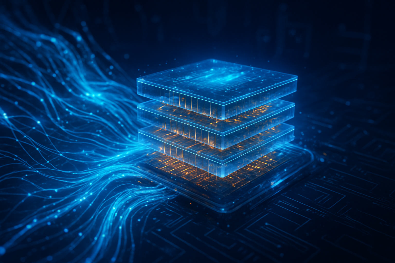
The HBM4 Breakthrough: Doubling the Data Highway
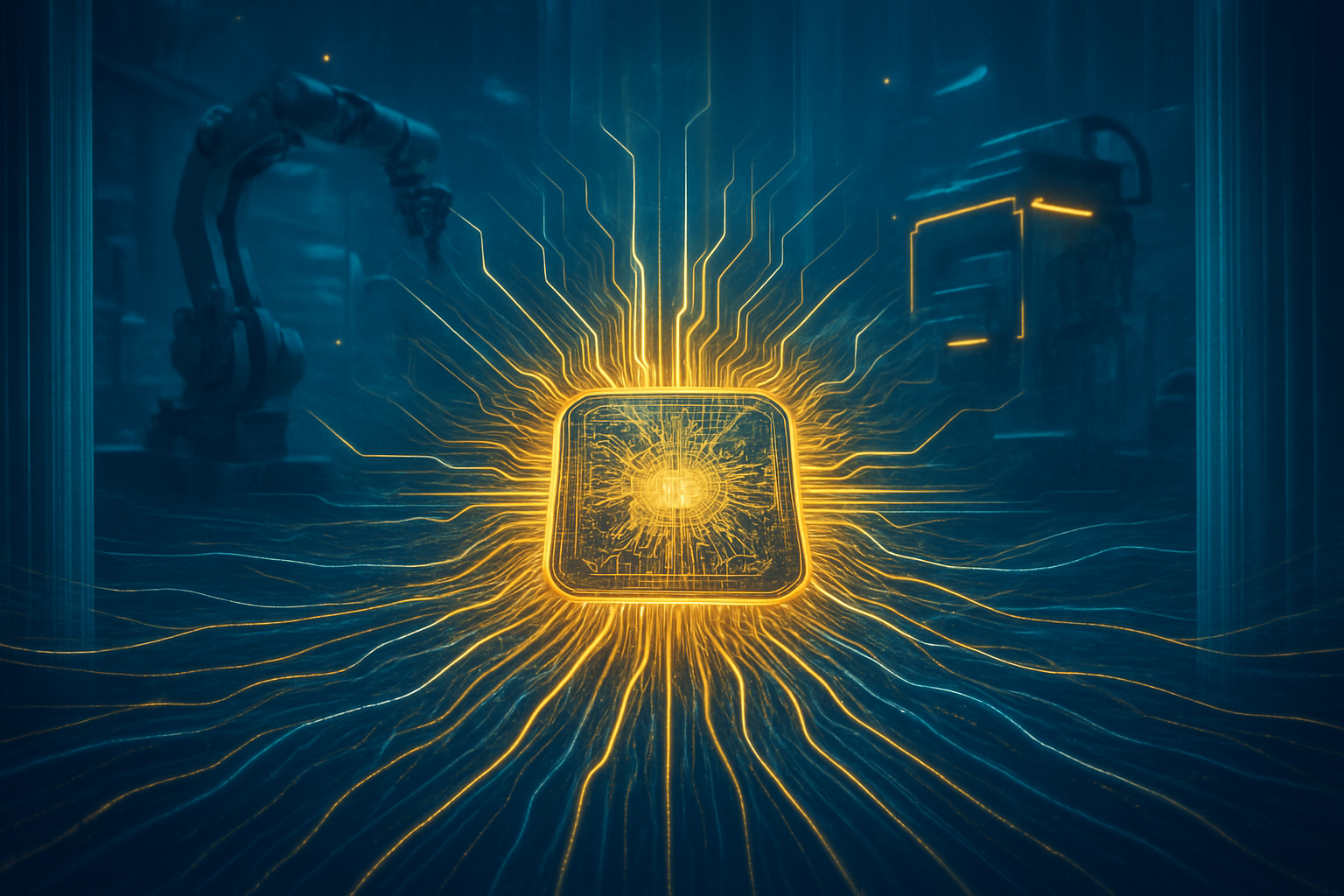
The defining characteristic of HBM4 is the doubling of the memory interface width from 1024-bit to 2048-bit. This "GPT-4 moment" for hardware allows for a massive leap in data throughput without the exponential power consumption increases that plagued late-stage HBM3E. Current 2026 specifications show HBM4 stacks reaching bandwidths between 2.0 TB/s and 2.8 TB/s per stack. Samsung has taken an early lead in volume, having secured Production Readiness Approval (PRA) from NVIDIA in late 2025 and commencing mass production of 12-Hi (12-layer) HBM4 at its Pyeongtaek facility this month.
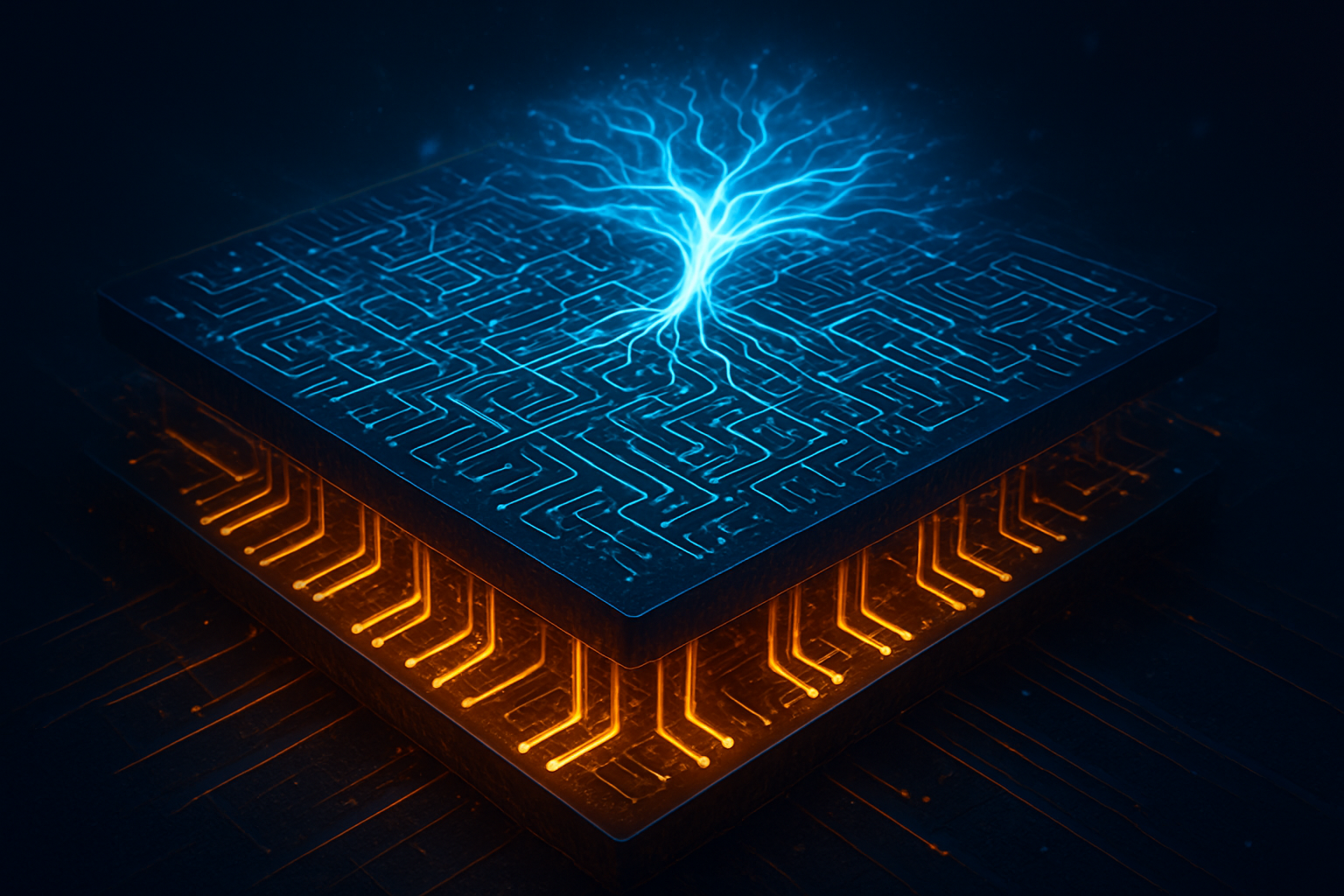
Technically, HBM4 introduces hybrid bonding and custom logic dies, moving away from the traditional micro-bump interface. This allows for a thinner profile and better thermal management, which is essential as GPUs now regularly exceed 1,000 watts of power draw. SK Hynix, which dominated the HBM3E cycle, has shifted its strategy to a "One-Team" alliance with Taiwan Semiconductor Manufacturing Company (NYSE: TSM), utilizing TSMC’s 5nm and 3nm nodes for the base logic dies. This collaboration aims to provide a more "system-level" memory solution, though their full-scale volume ramp is not expected until the second quarter of 2026.
Initial reactions from the AI research community have been overwhelmingly positive, as the increased memory capacity directly translates to lower latency in inference. Experts at leading AI labs note that HBM4 is the first memory technology designed specifically for the "post-transformer" era, where the "memory wall"—the gap between processor speed and memory access—has been the single greatest hurdle to achieving real-time reasoning in models exceeding 50 trillion parameters.
The Strategic Battle: Samsung’s Resurgence and the SK Hynix-TSMC Alliance
The competitive landscape has shifted dramatically in early 2026. Samsung, which struggled to gain traction during the HBM3E transition, has leveraged its position as an integrated device manufacturer (IDM). By handling memory production, logic die design, and advanced packaging internally, Samsung has offered a "turnkey" HBM4 solution that has proven attractive to NVIDIA for its new Rubin R100 platform. This vertical integration has allowed Samsung to reclaim significant market share that it had previously lost to SK Hynix.
Meanwhile, Micron Technology has carved out a niche as the performance leader. In early January 2026, Micron confirmed that its entire HBM4 production capacity for the year is already sold out, largely due to massive pre-orders from hyperscalers like Microsoft and Google. Micron’s 1β (1-beta) DRAM process has allowed it to achieve 2.8 TB/s speeds, slightly edging out the standard JEDEC specifications and making its stacks the preferred choice for high-frequency trading and specialized scientific research clusters.
The implications for AI labs are profound. The scarcity of HBM4 means that only the most well-funded organizations will have access to the hardware necessary to train 100-trillion parameter models in a reasonable timeframe. This reinforces the "compute moat" held by tech giants, as the cost of a single HBM4-equipped GPU node is expected to rise by 30% compared to the previous generation. However, the increased efficiency of HBM4 may eventually lower the total cost of ownership by reducing the number of nodes required to maintain the same level of performance.
Breaking the Memory Wall: Scaling to 100-Trillion Parameters
The HBM4 capacity race is fundamentally about the feasibility of the next generation of AI. As we move into 2026, the industry is no longer satisfied with 1.8-trillion parameter models like GPT-4. The goal is now 100 trillion parameters—a scale that mimics the complexity of the human brain's synaptic connections. Such models require multi-terabyte memory pools just to store their weights. Without HBM4’s 2048-bit interface and 64GB-per-stack capacity, these models would be forced to rely on slower inter-chip communication, leading to "stuttering" in AI reasoning.
Compared to previous milestones, such as the introduction of HBM2 or HBM3, the move to HBM4 is seen as a more significant structural shift. It marks the first time that memory manufacturers are becoming "co-designers" of the AI processor. The use of custom logic dies means that the memory is no longer a passive storage bin but an active participant in data pre-processing. This helps address the "thermal ceiling" that threatened to stall GPU development in 2024 and 2025.
However, concerns remain regarding the environmental impact and supply chain fragility. The manufacturing process for HBM4 is significantly more complex and has lower yields than standard DDR5 memory. This has led to a "bifurcation" of the semiconductor market, where resources are being diverted away from consumer electronics to feed the AI beast. Analysts warn that any disruption in the supply of high-purity chemicals or specialized packaging equipment could halt the production of HBM4, potentially causing a global "AI winter" driven by hardware shortages rather than a lack of algorithmic progress.
Beyond HBM4: The Roadmap to HBM5 and "Feynman" Architectures
Even as HBM4 begins its mass-market rollout, the industry is already looking toward HBM5. SK Hynix recently unveiled its 2029-2031 roadmap, confirming that HBM5 has moved into the formal design phase. Expected to debut around 2028, HBM5 is projected to feature a 4096-bit interface—doubling the width again—and utilize "bumpless" copper-to-copper direct bonding. This will likely support NVIDIA’s rumored "Feynman" architecture, which aims for a 10x increase in compute density over the current Rubin platform.
In the near term, 2027 will likely see the introduction of HBM4E (Extended), which will push stack heights to 16-Hi and 20-Hi. This will enable a single GPU to carry over 1TB of high-bandwidth memory. Such a development would allow for "edge AI" servers to run massive models locally, potentially solving many of the privacy and latency issues currently associated with cloud-based AI.
The challenge moving forward will be cooling. As memory stacks get taller and more dense, the heat generated in the middle of the stack becomes difficult to dissipate. Experts predict that 2026 and 2027 will see a surge in liquid-to-chip cooling adoption in data centers to accommodate these HBM4-heavy systems. The "memory-centric" era of computing is here, and the innovations in HBM5 will likely focus as much on thermal physics as on electrical engineering.
A New Era of Compute: Final Thoughts
The HBM4 capacity race of 2026 marks the end of general-purpose hardware dominance in the data center. We have entered an era where memory is the primary differentiator of AI capability. Samsung’s aggressive return to form, SK Hynix’s strategic alliance with TSMC, and Micron’s sold-out performance lead all point to a market that is maturing but remains incredibly volatile.
In the history of AI, the HBM4 transition will likely be remembered as the moment when hardware finally caught up to the ambitions of software architects. It provides the necessary foundation for the 100-trillion parameter models that will define the latter half of this decade. For the tech industry, the key takeaway is clear: the "Memory Wall" has not been demolished, but HBM4 has built a massive, high-speed bridge over it.
In the coming weeks and months, the industry will be watching the initial benchmarks of the NVIDIA Rubin R100 and the AMD Instinct MI400. These results will reveal which memory partner—Samsung, SK Hynix, or Micron—has delivered the best real-world performance. As 2026 unfolds, the success of these hardware platforms will determine the pace at which artificial general intelligence (AGI) moves from a theoretical goal to a practical reality.
This content is intended for informational purposes only and represents analysis of current AI developments.
TokenRing AI delivers enterprise-grade solutions for multi-agent AI workflow orchestration, AI-powered development tools, and seamless remote collaboration platforms.
For more information, visit https://www.tokenring.ai/.