As the calendar turns to 2026, the artificial intelligence industry stands on the precipice of its most significant hardware leap to date. NVIDIA (NASDAQ:NVDA) has officially moved into the production phase of its "Rubin" platform, the highly anticipated successor to the record-breaking Blackwell architecture. Named after the pioneering astronomer Vera Rubin, the new platform represents more than just a performance boost; it signals the definitive shift in NVIDIA’s strategy toward a relentless yearly release cadence, a move designed to maintain its stranglehold on the generative AI market and leave competitors in a state of perpetual catch-up.
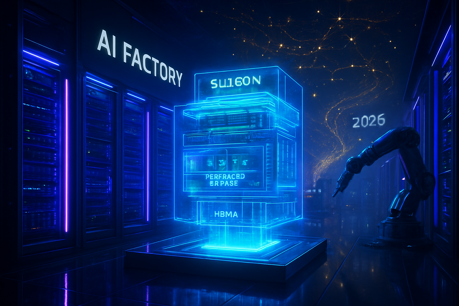
The immediate significance of the Rubin launch cannot be overstated. By integrating the new Vera CPU, the R100 GPU, and next-generation HBM4 memory, NVIDIA is attempting to solve the "memory wall" and "power wall" that have begun to slow the scaling of trillion-parameter models. For hyperscalers and AI research labs, the arrival of Rubin means the ability to train next-generation "Agentic AI" systems that were previously computationally prohibitive. This release marks the transition from AI as a software feature to AI as a vertically integrated industrial process, often referred to by NVIDIA CEO Jensen Huang as the era of "AI Factories."
Technical Mastery: Vera, Rubin, and the HBM4 Advantage
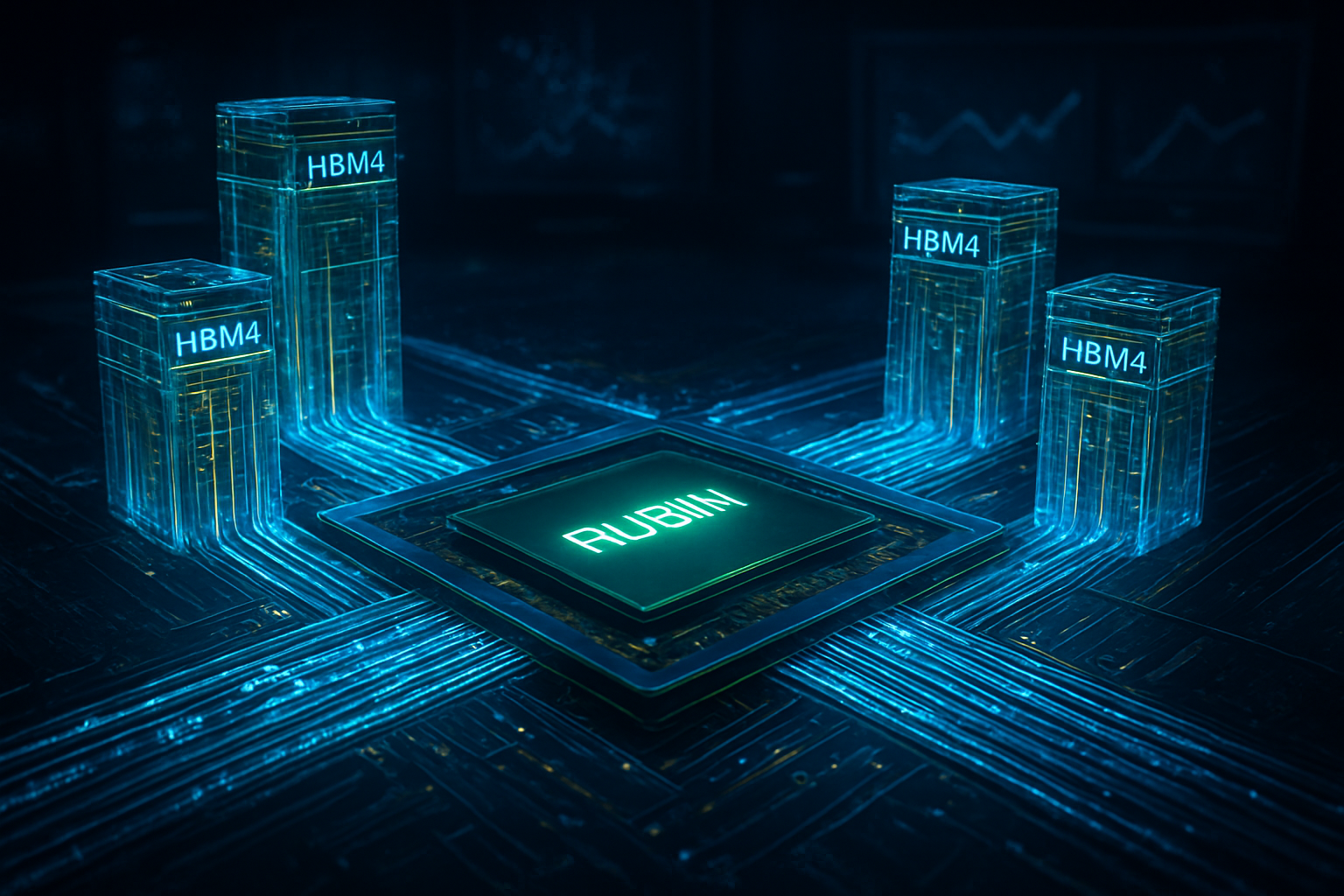
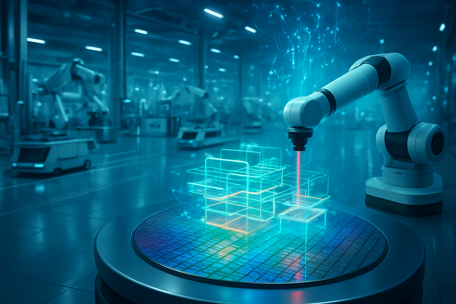
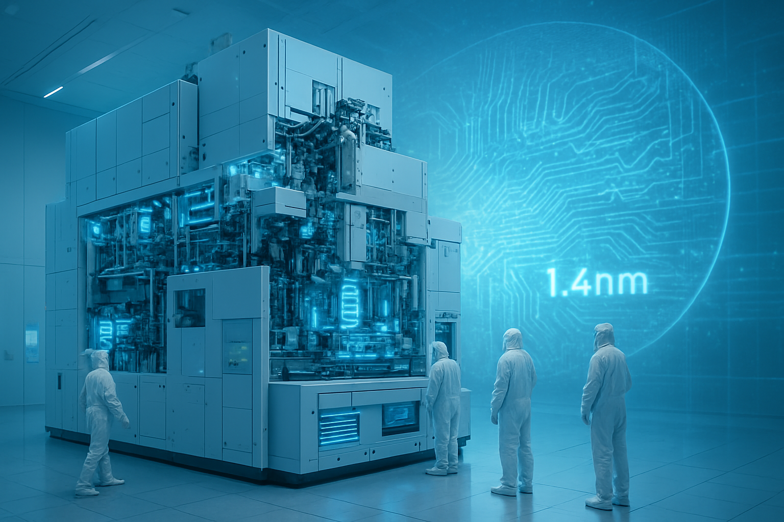
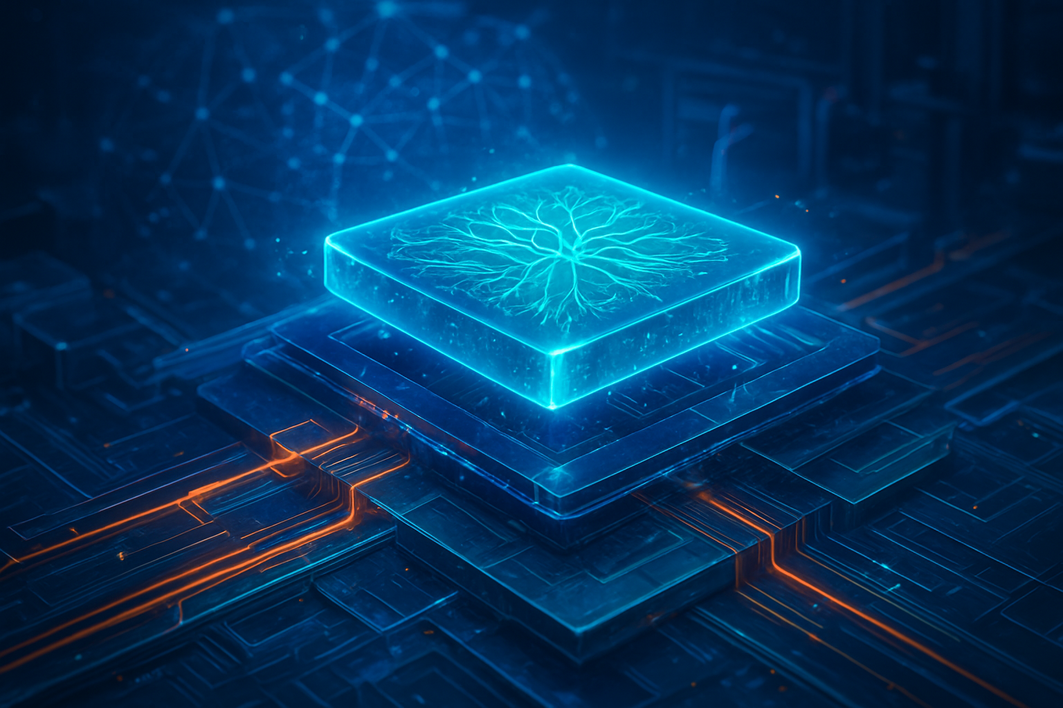
The technical core of the Rubin platform is the R100 GPU, a marvel of semiconductor engineering that moves away from the monolithic designs of the past. Fabricated on the performance-enhanced 3nm (N3P) process from TSMC (NYSE:TSM), the R100 utilizes advanced CoWoS-L packaging to bridge multiple compute dies into a single, massive logical unit. Early benchmarks suggest that a single R100 GPU can deliver up to 50 Petaflops of FP4 compute—a staggering 2.5x increase over the Blackwell B200. This leap is made possible by NVIDIA’s adoption of System on Integrated Chips (SoIC) 3D-stacking, which allows for vertical integration of logic and memory, drastically reducing the physical distance data must travel and lowering power "leakage" that has plagued previous generations.
A critical component of this architecture is the "Vera" CPU, which replaces the Grace CPU found in earlier superchips. Unlike its predecessor, which relied on standard Arm Neoverse designs, Vera is built on NVIDIA’s custom "Olympus" ARM cores. This transition to custom silicon allows for much tighter optimization between the CPU and GPU, specifically for the complex data-shuffling tasks required by multi-agent AI workflows. The resulting "Vera Rubin" superchip pairs the Vera CPU with two R100 GPUs via a 3.6 TB/s NVLink-6 interconnect, providing the bidirectional bandwidth necessary to treat the entire rack as a single, unified computer.
Memory remains the most significant bottleneck in AI training, and Rubin addresses this by being the first architecture to fully adopt the HBM4 standard. These memory stacks, provided by lead partners like SK Hynix (KRX:000660) and Samsung (KRX:005930), offer a massive jump in both capacity and throughput. Standard R100 configurations now feature 288GB of HBM4, with "Ultra" versions expected to reach 512GB later this year. By utilizing a customized logic base die—co-developed with TSMC—the HBM4 modules are integrated directly onto the GPU package, allowing for bandwidth speeds exceeding 13 TB/s. This allows the Rubin platform to handle the massive KV caches required for the long-context windows that define 2026-era large language models.
Initial reactions from the AI research community have been a mix of excitement and logistical concern. While the performance gains are undeniable, the power requirements for a full Rubin-based NVL144 rack are projected to exceed 500kW. Industry experts note that while NVIDIA has solved the compute problem, they have placed a massive burden on data center infrastructure. The shift to liquid cooling is no longer optional for Rubin adopters; it is a requirement. Researchers at major labs have praised the platform's deterministic processing capabilities, which aim to close the "inference gap" and allow for more reliable real-time reasoning in AI agents.
Shifting the Industry Paradigm: The Impact on Hyperscalers and Competitors
The launch of Rubin significantly alters the competitive landscape for the entire tech sector. For hyperscalers like Microsoft (NASDAQ:MSFT), Alphabet (NASDAQ:GOOGL), and Amazon (NASDAQ:AMZN), the Rubin platform is both a blessing and a strategic challenge. These companies are the primary purchasers of NVIDIA hardware, yet they are also developing their own custom AI silicon, such as Maia, TPU, and Trainium. NVIDIA’s shift to a yearly cadence puts immense pressure on these internal projects; if a cloud provider’s custom chip takes two years to develop, it may be two generations behind NVIDIA’s latest offering by the time it reaches the data center.
Major AI labs, including OpenAI and Meta (NASDAQ:META), stand to benefit the most from the Rubin rollout. Meta, in particular, has been aggressive in its pursuit of massive compute clusters to power its Llama series of models. The increased memory bandwidth of HBM4 will allow these labs to move beyond static LLMs toward "World Models" that require high-speed video processing and multi-modal reasoning. However, the sheer cost of Rubin systems—estimated to be 20-30% higher than Blackwell—further widens the gap between the "compute-rich" elite and smaller AI startups, potentially centralizing AI power into fewer hands.
For direct hardware competitors like AMD (NASDAQ:AMD) and Intel (NASDAQ:INTC), the Rubin announcement is a formidable hurdle. AMD’s MI300 and MI400 series have gained some ground by offering competitive memory capacities, but NVIDIA’s vertical integration of the Vera CPU and NVLink networking makes it difficult for "GPU-only" competitors to match system-level efficiency. To compete, AMD and Intel are increasingly looking toward open standards like the Ultra Accelerator Link (UALink), but NVIDIA’s proprietary ecosystem remains the gold standard for performance. Meanwhile, memory manufacturers like Micron (NASDAQ:MU) are racing to ramp up HBM4 production to meet the insatiable demand created by the Rubin production cycle.
The market positioning of Rubin also suggests a strategic pivot toward "Sovereign AI." NVIDIA is increasingly selling entire "AI Factory" blueprints to national governments in the Middle East and Southeast Asia. These nations view the Rubin platform not just as hardware, but as a foundation for national security and economic independence. By providing a turnkey solution that includes compute, networking, and software (CUDA), NVIDIA has effectively commoditized the supercomputer, making it accessible to any entity with the capital to invest in the 2026 hardware cycle.
Scaling the Future: Energy, Efficiency, and the AI Arms Race
The broader significance of the Rubin platform lies in its role as the engine of the "AI scaling laws." For years, the industry has debated whether increasing compute and data would continue to yield intelligence gains. Rubin is NVIDIA’s bet that the ceiling is nowhere in sight. By delivering a 2.5x performance jump in a single generation, NVIDIA is effectively attempting to maintain a "Moore’s Law for AI," where compute power doubles every 12 to 18 months. This rapid advancement is essential for the transition from generative AI—which creates content—to agentic AI, which can plan, reason, and execute complex tasks autonomously.
However, this progress comes with significant environmental and infrastructure concerns. The energy density of Rubin-based data centers is forcing a radical rethink of the power grid. We are seeing a trend where AI companies are partnering directly with energy providers to build "nuclear-powered" data centers, a concept that seemed like science fiction just a few years ago. The Rubin platform’s reliance on liquid cooling and specialized power delivery systems means that the "AI arms race" is no longer just about who has the best algorithms, but who has the most robust physical infrastructure.
Comparisons to previous AI milestones, such as the 2012 AlexNet moment or the 2017 "Attention is All You Need" paper, suggest that we are currently in the "Industrialization Phase" of AI. If Blackwell was the proof of concept for trillion-parameter models, Rubin is the production engine for the trillion-agent economy. The integration of the Vera CPU is particularly telling; it suggests that the future of AI is not just about raw GPU throughput, but about the sophisticated orchestration of data between various compute elements. This holistic approach to system design is what separates the current era from the fragmented hardware landscapes of the past decade.
There is also a growing concern regarding the "silicon ceiling." As NVIDIA moves to 3nm and looks toward 2nm for future architectures, the physical limits of transistor shrinking are becoming apparent. Rubin’s reliance on "brute-force" scaling—using massive packaging and multi-die configurations—indicates that the industry is moving away from traditional semiconductor scaling and toward "System-on-a-Chiplet" architectures. This shift ensures that NVIDIA remains at the center of the ecosystem, as they are one of the few companies with the scale and expertise to manage the immense complexity of these multi-die systems.
The Road Ahead: Beyond Rubin and the 2027 Roadmap
Looking forward, the Rubin platform is only the beginning of NVIDIA's 2026–2028 roadmap. Following the initial R100 rollout, NVIDIA is expected to launch the "Rubin Ultra" in 2027. This refresh will likely feature HBM4e (extended) memory and even higher interconnect speeds, targeting the training of models with 100 trillion parameters or more. Beyond that, early leaks have already begun to mention the "Feynman" architecture for 2028, named after the physicist Richard Feynman, which is rumored to explore even more exotic computing paradigms, possibly including early-stage photonic interconnects.
The potential applications for Rubin-class compute are vast. In the near term, we expect to see a surge in "Real-time Digital Twins"—highly accurate, AI-powered simulations of entire cities or industrial supply chains. In healthcare, the Rubin platform’s ability to process massive genomic and proteomic datasets in real-time could lead to the first truly personalized, AI-designed medicines. However, the challenge remains in the software; as hardware capabilities explode, the burden shifts to developers to create software architectures that can actually utilize 50 Petaflops of compute without being throttled by data bottlenecks.
Experts predict that the next two years will be defined by a "re-architecting" of the data center. As Rubin becomes the standard, we will see a move away from general-purpose cloud computing toward specialized "AI Clouds" that are physically optimized for the Vera Rubin superchips. The primary challenge will be the supply chain; while NVIDIA has booked significant capacity at TSMC, any geopolitical instability in the Taiwan Strait remains the single greatest risk to the Rubin rollout and the broader AI economy.
A New Benchmark for the Intelligence Age
The arrival of the NVIDIA Rubin platform marks a definitive turning point in the history of computing. By moving to a yearly release cadence and integrating custom CPU cores with HBM4 memory, NVIDIA has not only set a new performance benchmark but has fundamentally redefined what a "computer" is in the age of artificial intelligence. Rubin is no longer just a component; it is the central nervous system of the modern AI factory, providing the raw power and sophisticated orchestration required to move toward true machine intelligence.
The key takeaway from the Rubin launch is that the pace of AI development is accelerating, not slowing down. For businesses and governments, the message is clear: the window for adopting and integrating these technologies is shrinking. Those who can harness the power of the Rubin platform will have a decisive advantage in the coming "Agentic Era," while those who hesitate risk being left behind by a hardware cycle that no longer waits for anyone.
In the coming weeks and months, the industry will be watching for the first production benchmarks from "Rubin-powered" clusters and the subsequent response from the "Open AI" ecosystem. As the first Rubin units begin shipping to early-access customers this quarter, the world will finally see if this massive investment in silicon and power can deliver on the promise of the next great leap in human-machine collaboration.
This content is intended for informational purposes only and represents analysis of current AI developments.
TokenRing AI delivers enterprise-grade solutions for multi-agent AI workflow orchestration, AI-powered development tools, and seamless remote collaboration platforms.
For more information, visit https://www.tokenring.ai/.