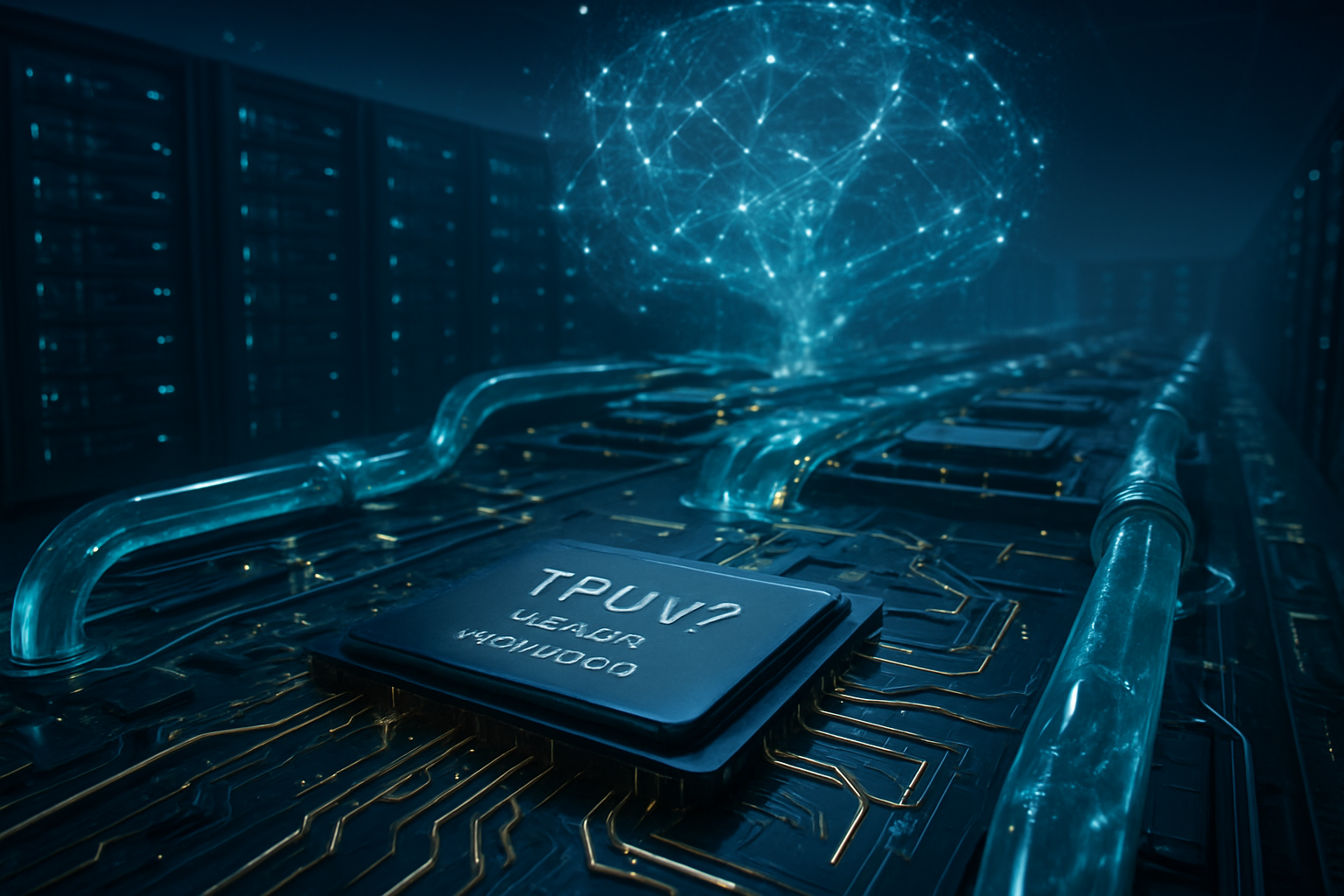
In a move that signals a seismic shift in the cloud computing landscape, Microsoft (NASDAQ: MSFT) has officially unveiled the Maia 200, its second-generation custom AI accelerator designed specifically to power the next frontier of generative AI. Announced in late January 2026, the Maia 200 marks a significant departure from general-purpose hardware, prioritizing an "inference-first" architecture that aims to drastically reduce the cost and energy consumption of running massive models like those from OpenAI.
The arrival of the Maia 200 is not merely a hardware update; it is a strategic maneuver to de-risk Microsoft’s reliance on third-party silicon providers while optimizing the economics of its Azure AI infrastructure. By moving beyond the general-purpose limitations of traditional GPUs, Microsoft is positioning itself to handle the "inference era," where the primary challenge for tech giants is no longer just training models, but serving billions of AI-generated tokens to users at a sustainable price point.
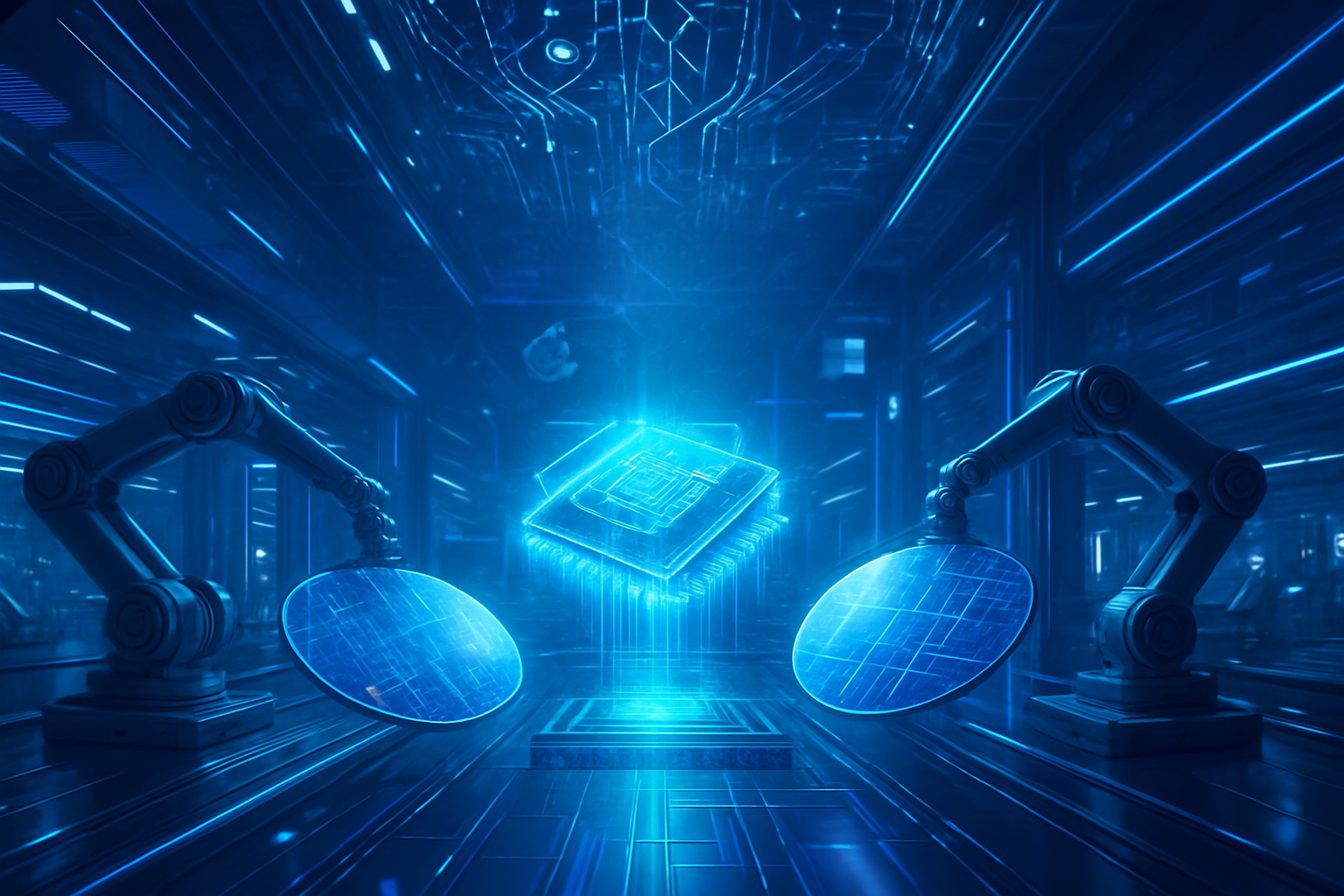
The Technical Edge: Precision, Memory, and the 3nm Powerhouse
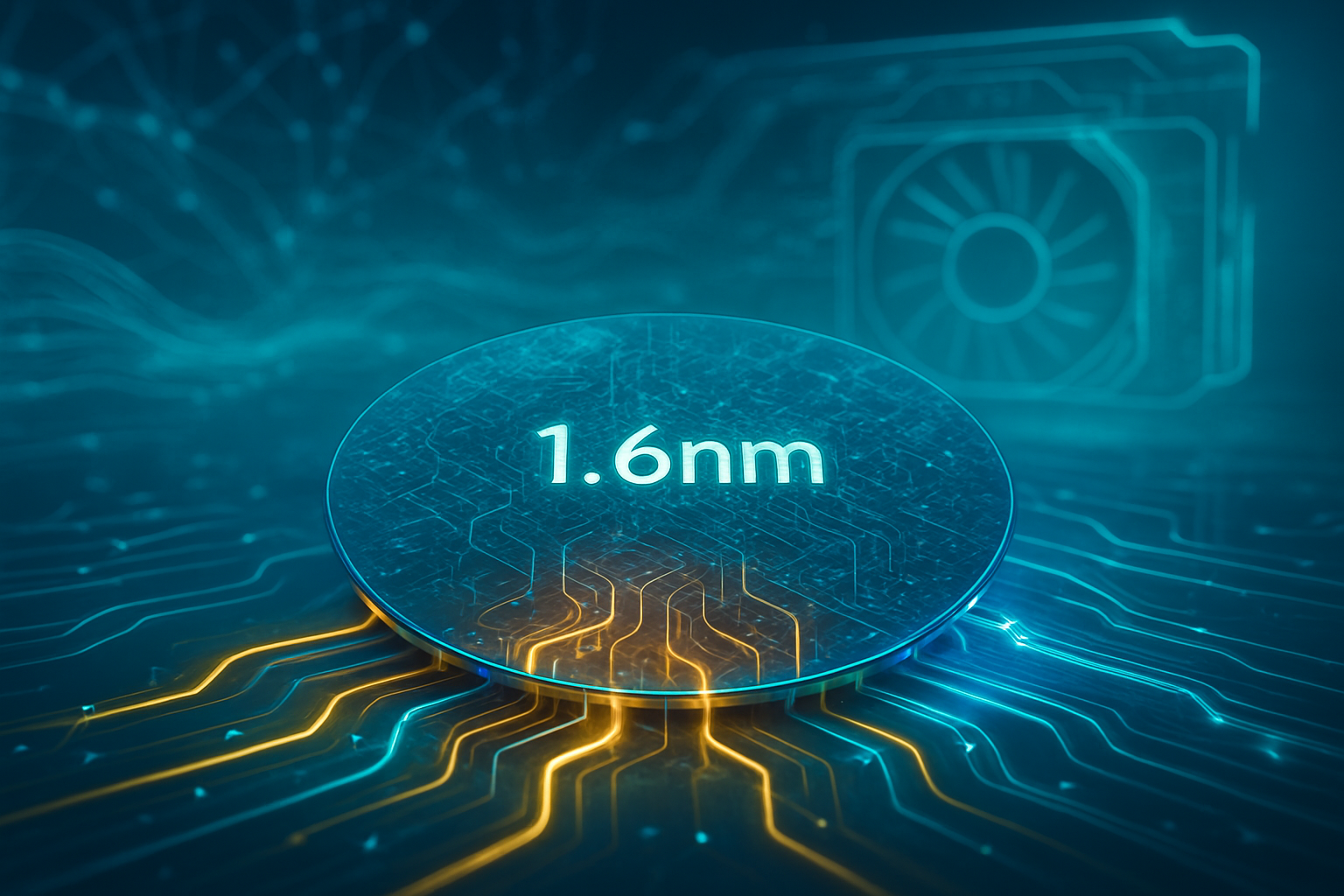
The Maia 200 is an Application-Specific Integrated Circuit (ASIC) built on TSMC’s cutting-edge 3nm (N3P) process node, packing approximately 140 billion transistors into its silicon. Unlike general-purpose GPUs that must allocate die area for a wide range of graphical and scientific computing tasks, the Maia 200 is laser-focused on the mathematics of large language models (LLMs). At its core, the chip utilizes an "inference-first" design philosophy, natively supporting FP4 (4-bit) and FP8 (8-bit) tensor formats. These low-precision formats allow for massive throughput—reaching a staggering 10.15 PFLOPS in FP4 compute—while minimizing the energy required for each calculation.
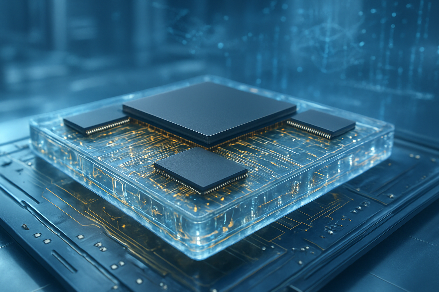
Perhaps the most critical technical advancement is how the Maia 200 addresses the "memory wall"—the bottleneck where the speed of AI generation is limited by how fast data can move from memory to the processor. Microsoft has equipped the chip with 216 GB of HBM3e memory and a massive 7 TB/s of bandwidth. To put this in perspective, this is significantly higher than the memory bandwidth offered by many high-end general-purpose GPUs from previous years, such as the NVIDIA (NASDAQ: NVDA) H100. This specialized memory architecture allows the Maia 200 to host larger, more complex models on a single chip, reducing the latency associated with inter-chip communication.
Furthermore, the Maia 200 is designed for "heterogeneous infrastructure." It is not intended to replace the NVIDIA Blackwell or AMD (NASDAQ: AMD) Instinct GPUs in Microsoft’s fleet but rather to work alongside them. Microsoft’s software stack, including the Maia SDK and Triton compiler integration, allows developers to seamlessly move workloads between different hardware types. This interoperability ensures that Azure customers can choose the most cost-effective hardware for their specific model's needs, whether it be high-intensity training or high-volume inference.
Reshaping the Competitive Landscape of Cloud Silicon
The introduction of the Maia 200 has immediate implications for the competitive dynamics between cloud providers and chipmakers. By vertically integrating its hardware and software, Microsoft is following in the footsteps of Apple and Google (NASDAQ: GOOGL), seeking to capture the "silicon margin" that usually goes to third-party vendors. For Microsoft, the benefit is twofold: a reported 30% improvement in performance-per-dollar and a significant reduction in the total cost of ownership (TCO) for running its flagship Copilot and OpenAI services.
For AI labs and startups, this development is a harbinger of more affordable compute. As Microsoft scales the Maia 200 across its global data centers—starting with regions in the U.S. and expanding rapidly—the cost of accessing frontier models like the GPT-5.2 family is expected to drop. This puts immense pressure on competitors like Amazon (NASDAQ: AMZN), whose Trainium and Inferentia chips are now in a direct performance arms race with Microsoft’s custom silicon. Industry experts suggest that the Maia 200’s specialized design gives Microsoft a unique "home-court advantage" in optimizing its own proprietary models, such as the Phi series and the vast array of Copilot agents.
Market analysts believe this vertical integration strategy serves as a hedge against supply chain volatility. While NVIDIA remains the king of the training market, the Maia 200 allows Microsoft to stabilize its supply of inference hardware. This strategic independence is vital for a company that is betting its future on the ubiquity of AI-powered productivity tools. By owning the chip, the cooling system, and the software stack, Microsoft can optimize every watt of power used in its Azure data centers, which is increasingly critical as energy availability becomes the primary bottleneck for AI expansion.
Efficiency as the New North Star in the AI Landscape
The shift from "raw power" to "efficiency" represented by the Maia 200 reflects a broader trend in the AI landscape. In the early 2020s, the focus was on the size of the model and the sheer number of GPUs needed to train it. In 2026, the industry is pivoting toward sustainability and cost-per-token. The Maia 200's focus on performance-per-watt is a direct response to the massive energy demands of global AI usage. At a TDP (Thermal Design Power) of 750W, it is high-powered hardware, but the sheer amount of work it performs per watt far exceeds previous general-purpose solutions.
This development also highlights the growing importance of "agentic AI"—AI systems that can reason and execute multi-step tasks. These models require consistent, low-latency token generation to feel responsive to users. The Maia 200's Mesh Network-on-Chip (NoC) is specifically optimized for these predictable but intense dataflows. In comparison to previous milestones, like the initial release of GPT-4, the release of the Maia 200 represents the "industrialization" of AI—the phase where the focus turns from "can we do it?" to "how can we do it for everyone, everywhere, at scale?"
However, this trend toward custom silicon also raises concerns about vendor lock-in. While Microsoft’s use of open-source compilers like Triton helps mitigate this, the deepest optimizations for the Maia 200 will likely remain proprietary. This could create a tiered cloud market where the most efficient way to run an OpenAI model is exclusively on Azure's custom chips, potentially limiting the portability of high-end AI applications across different cloud providers.
The Road Ahead: Agentic AI and Synthetic Data
Looking forward, the Maia 200 is expected to be the primary engine for Microsoft’s ambitious "Superintelligence" initiatives. One of the most anticipated near-term applications is the use of Maia-powered clusters for massive-scale synthetic data generation. As high-quality human data becomes increasingly scarce, the ability to efficiently generate millions of high-reasoning "thought traces" using FP4 precision will be essential for training the next generation of models.
Experts predict that we will soon see "Maia-exclusive" features within Azure, such as ultra-low-latency real-time translation and complex autonomous agents that require constant background computation. The long-term challenge for Microsoft will be keeping pace with the rapid evolution of AI architectures. While the Maia 200 is optimized for today's Transformer-based models, the potential emergence of new architectures, such as State Space Models (SSMs) or more advanced Liquid Neural Networks, will require the hardware to remain flexible. Microsoft’s commitment to a "heterogeneous" approach suggests they are prepared to pivot if the underlying math of AI changes again.
A Decisive Moment for Azure and the AI Economy
The Maia 200 represents a coming-of-age for Microsoft's silicon ambitions. It is a sophisticated piece of engineering that demonstrates how vertical integration can solve the most pressing problems in the AI industry: cost, energy, and scale. By building a chip that is "inference-first," Microsoft has acknowledged that the future of AI is not just about the biggest models, but about the most efficient ones.
As we look toward the remainder of 2026, the success of the Maia 200 will be measured by its ability to keep Copilot affordable and its role in enabling the next generation of OpenAI’s "reasoning" models. The tech industry should watch closely as these chips roll out across more Azure regions, as this will likely be the catalyst for a new round of price wars in the AI cloud market. The "inference wars" have officially begun, and with Maia 200, Microsoft has fired a formidable opening shot.
This content is intended for informational purposes only and represents analysis of current AI developments.
TokenRing AI delivers enterprise-grade solutions for multi-agent AI workflow orchestration, AI-powered development tools, and seamless remote collaboration platforms.
For more information, visit https://www.tokenring.ai/.