Tag: AI Hardware

  • Beijing’s Silent Mandate: China Enforces 50% Domestic Tool Rule to Shield AI Ambitions

    Beijing’s Silent Mandate: China Enforces 50% Domestic Tool Rule to Shield AI Ambitions

    In a move that signals a decisive shift in the global technology cold war, Beijing has informally implemented a strict 50% domestic semiconductor equipment mandate for all new chip-making capacity. This "window guidance," enforced through the state’s rigorous approval process for new fabrication plants, requires domestic chipmakers to source at least half of their manufacturing tools from local suppliers. The directive is a cornerstone of China’s broader strategy to immunize its domestic artificial intelligence and high-performance computing sectors against escalating Western export controls.

    The significance of this mandate cannot be overstated. By creating a guaranteed market for domestic champions, China is accelerating its transition from a buyer of foreign technology to a self-sufficient powerhouse. This development directly supports the production of advanced silicon necessary for the next generation of large language models (LLMs) and autonomous systems, ensuring that China’s AI roadmap remains unhindered by geopolitical friction.

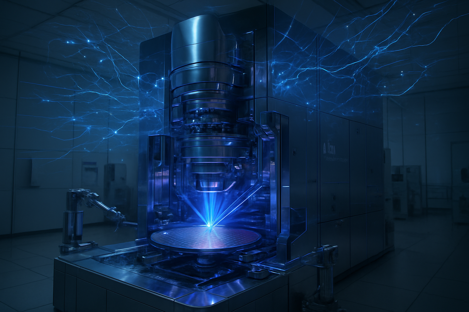
    Breakthroughs in the Clean Room: 7nm Testing and Localized Etching

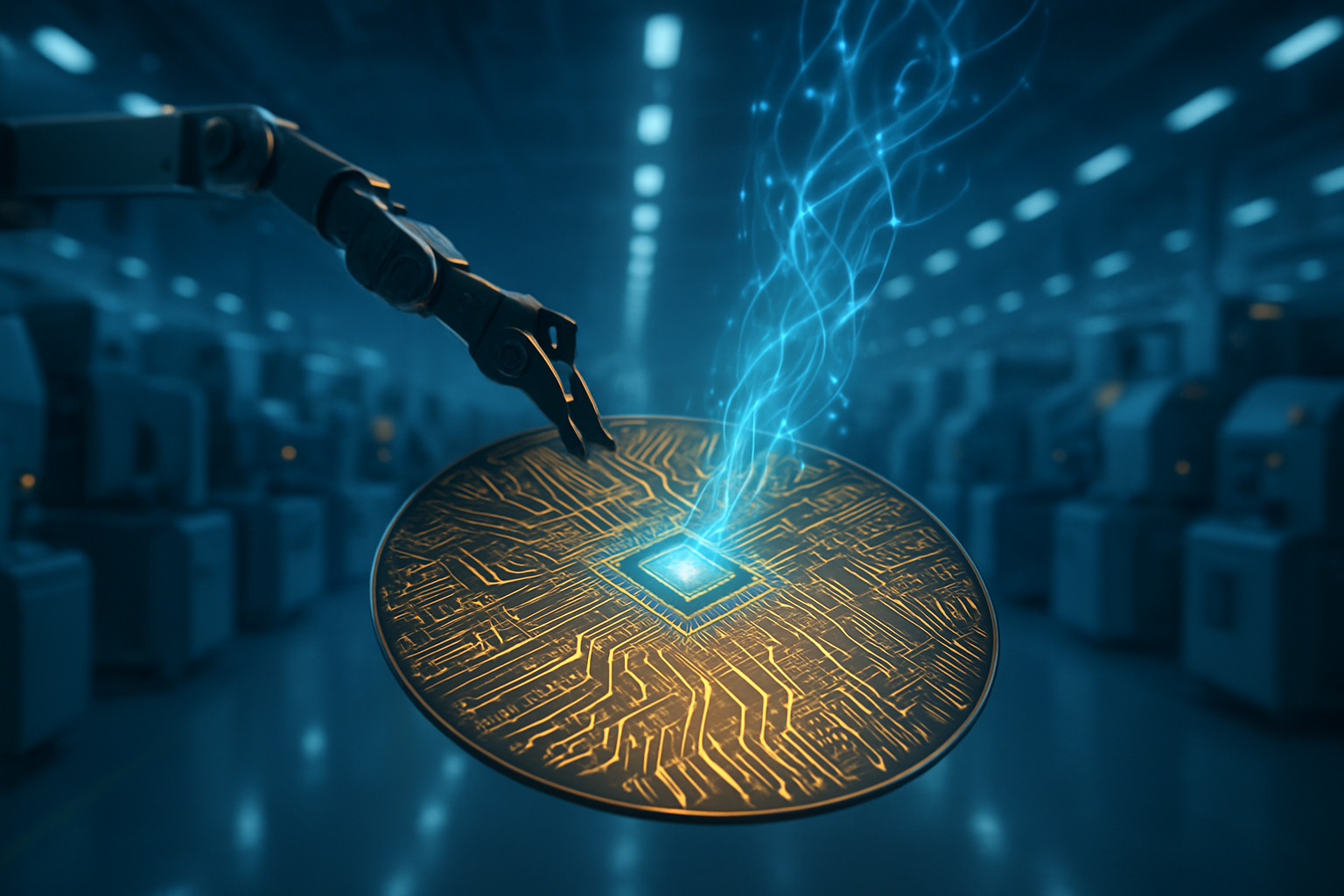
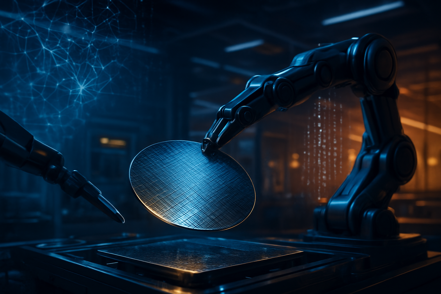
    The technical heart of this mandate lies in the rapid advancement of etching and cleaning technologies, sectors once dominated by American and Japanese firms. Reports as of late 2025 confirm that Semiconductor Manufacturing International Corporation (HKG: 0981), or SMIC, has successfully integrated domestic etching tools into its 7nm production lines for pilot testing. These tools, primarily supplied by Naura Technology Group (SZSE: 002371), are performing critical "patterning" tasks that define the microscopic architecture of advanced AI accelerators. This represents a significant leap from just two years ago, when domestic tools were largely relegated to "mature" nodes of 28nm and above.

    Unlike previous self-sufficiency attempts that focused on low-end hardware, the current push emphasizes "learning-by-doing" on advanced nodes. In addition to etching, China has achieved nearly 50% self-sufficiency in cleaning and photoresist-removal tools. Firms like ACM Research (Shanghai) and Naura have developed advanced single-wafer cleaning systems that are now being integrated into SMIC’s most sophisticated process flows. These tools are essential for maintaining the high yields required for 7nm and 5nm production, where even a single microscopic particle can ruin a multi-thousand-dollar AI chip.

    Initial reactions from the global semiconductor research community suggest a mix of surprise and concern. While Western experts previously argued that China was decades away from replicating the precision of high-end etching gear, the sheer volume of state-backed R&D—bolstered by the $47.5 billion "Big Fund" Phase III—has compressed this timeline. The ability to test these tools in real-world, high-volume environments like SMIC’s fabs provides a feedback loop that is rapidly closing the performance gap with Western counterparts.

    The Great Decoupling: Market Winners and the Squeeze on US Giants

    The 50% mandate has created a bifurcated market where domestic firms are experiencing explosive growth at the expense of established Silicon Valley titans. Naura Technology Group has recently ascended to become the world’s sixth-largest semiconductor equipment maker, reporting a 30% revenue jump in the first half of 2025. Similarly, Advanced Micro-Fabrication Equipment Inc. (SSE: 688012), known as AMEC, has seen its revenue soar by 44%, driven by its specialized Capacitively Coupled Plasma (CCP) etching tools which are now capable of handling nearly all etching steps for 5nm processes.

    Conversely, the impact on U.S. equipment makers has transitioned from a temporary setback to a structural exclusion. Applied Materials, Inc. (NASDAQ: AMAT) has estimated a $710 million hit to its fiscal 2026 revenue as its share of the Chinese market continues to dwindle. Lam Research Corporation (NASDAQ: LRCX), which specializes in the very etching tools that AMEC and Naura are now replicating, has seen its China-based revenue drop significantly as local fabs swap out foreign gear for "good enough" domestic alternatives.

    Even firms that were once considered indispensable are feeling the pressure. While KLA Corporation (NASDAQ: KLAC) remains more resilient due to the extreme complexity of metrology and inspection tools, it now faces long-term competition from state-funded Chinese startups like Hwatsing and RSIC. The strategic advantage has shifted: Chinese chipmakers are no longer just buying tools; they are building a protected ecosystem that ensures their long-term survival in the AI era, regardless of future sanctions from Washington or The Hague.

    AI Sovereignty and the "Whole-Nation" Strategy

    This mandate is a critical component of China's broader AI landscape, where hardware sovereignty is viewed as a prerequisite for national security. By forcing a 50% domestic adoption rate, Beijing is ensuring that its AI industry is not built on a "foundation of sand." If the U.S. were to further restrict the export of tools from companies like ASML Holding N.V. (NASDAQ: ASML) or Tokyo Electron, China’s existing domestic capacity would act as a vital buffer, allowing for the continued production of the Ascend and Biren AI chips that power its domestic data centers.

    The move mirrors previous industrial milestones, such as China’s rapid dominance in the high-speed rail and solar panel industries. By utilizing a "whole-nation" approach, the government is absorbing the initial costs of lower-performing domestic tools to provide the scale necessary for technological convergence. This strategy addresses the primary concern of many industry analysts: that domestic tools might initially lead to lower yields. Beijing’s response is clear—yields can be improved through iteration, but a total cutoff from foreign technology cannot be easily mitigated without a local manufacturing base.

    However, this aggressive push toward self-sufficiency also raises concerns about global supply chain fragmentation. As China moves toward its 100% domestic goal, the global semiconductor industry risks splitting into two incompatible ecosystems. This could lead to increased costs for AI development globally, as the economies of scale provided by a unified global market begin to erode.

    The Road to 100%: What Lies Ahead

    Looking toward the near-term, industry insiders expect the 50% threshold to be just the beginning. Under the 15th Five-Year Plan (2026–2030), Beijing is projected to raise the informal mandate to 70% or higher by 2027. The ultimate goal is 100% domestic equipment for the entire supply chain, including the most challenging frontier: Extreme Ultraviolet (EUV) lithography. While China still lags significantly in lithography, the progress made in etching and cleaning provides a blueprint for how they intend to tackle the rest of the stack.

    The next major challenge will be the development of local alternatives for high-end metrology and chemical mechanical polishing (CMP) tools. Experts predict that the next two years will see a flurry of domestic acquisitions and state-led mergers as China seeks to consolidate its fragmented equipment sector into a few "national champions" capable of competing with the likes of Applied Materials on a global stage.

    A Final Assessment of the Semiconductor Shift

    The implementation of the 50% domestic equipment mandate marks a point of no return for the global chip industry. China has successfully leveraged its massive internal market to force a technological evolution that many thought was impossible under the weight of Western sanctions. By securing the tools of production, Beijing is effectively securing its future in artificial intelligence, ensuring that its researchers and companies have the silicon necessary to compete in the global AI race.

    In the coming weeks and months, investors and policy analysts should watch for the official release of the 15th Five-Year Plan details, which will likely codify these informal mandates into long-term national policy. The era of a globalized, borderless semiconductor supply chain is ending, replaced by a new reality of "silicon nationalism" where the ability to build the machine that builds the chip is the ultimate form of power.


    This content is intended for informational purposes only and represents analysis of current AI developments.

    TokenRing AI delivers enterprise-grade solutions for multi-agent AI workflow orchestration, AI-powered development tools, and seamless remote collaboration platforms.
    For more information, visit https://www.tokenring.ai/.

  • The Great Silicon Decoupling: How RISC-V Became the Geopolitical Pivot of Global Computing in 2025

    The Great Silicon Decoupling: How RISC-V Became the Geopolitical Pivot of Global Computing in 2025

    As of December 29, 2025, the global semiconductor landscape has reached a definitive turning point, marked by the meteoric rise of the open-source RISC-V architecture. Long viewed as a niche academic project or a low-power alternative for simple microcontrollers, RISC-V has officially matured into the "third pillar" of the industry, challenging the long-standing duopoly held by x86 and ARM Holdings (NASDAQ: ARM). Driven by a volatile cocktail of geopolitical trade restrictions, a global push for chip self-sufficiency, and the insatiable demand for custom AI accelerators, RISC-V now commands an unprecedented 25% of the global System-on-Chip (SoC) market.

    The significance of this shift cannot be overstated. For decades, the foundational blueprints of computing were locked behind proprietary licenses, leaving nations and corporations vulnerable to shifting trade policies and escalating royalty fees. However, in 2025, the "royalty-free" nature of RISC-V has transformed it from a technical choice into a strategic imperative. From the data centers of Silicon Valley to the state-backed foundries of Shenzhen, the architecture is being utilized to bypass traditional export controls, enabling a new era of "sovereign silicon" that is fundamentally reshaping the balance of power in the digital age.

    The Technical Ascent: From Embedded Roots to Data Center Dominance

    The technical narrative of 2025 is dominated by the arrival of high-performance RISC-V cores that rival the best of proprietary designs. A major milestone was reached this month with the full-scale deployment of the third-generation XiangShan CPU, developed by the Chinese Academy of Sciences. Utilizing the "Kunminghu" architecture, benchmarks released in late 2025 indicate that this open-source processor has achieved performance parity with the ARM Neoverse N2, proving that the collaborative, open-source model can produce world-class server-grade silicon. This breakthrough has silenced critics who once argued that RISC-V could never compete in high-performance computing (HPC) environments.

    Further accelerating this trend is the maturation of the RISC-V Vector (RVV) 1.0 extensions, which have become the gold standard for specialized AI workloads. Unlike the rigid instruction sets of Intel (NASDAQ: INTC) or ARM, RISC-V allows engineers to add custom "secret sauce" instructions to their chips without breaking compatibility with the broader software ecosystem. This extensibility was a key factor in NVIDIA (NASDAQ: NVDA) announcing its historic decision in July 2025 to port its proprietary CUDA platform to RISC-V. By allowing its industry-leading AI software stack to run on RISC-V host processors, NVIDIA has effectively decoupled its future from the x86 and ARM architectures that have dominated the data center for 40 years.

    The reaction from the AI research community has been overwhelmingly positive, as the open nature of the ISA allows for unprecedented transparency in hardware-software co-design. Experts at the recent RISC-V Industry Development Conference noted that the ability to "peek under the hood" of the processor architecture is leading to more efficient AI inference models. By tailoring the hardware directly to the mathematical requirements of Large Language Models (LLMs), companies are reporting up to a 40% improvement in energy efficiency compared to general-purpose legacy architectures.

    The Corporate Land Grab: Consolidation and Competition

    The corporate world has responded to the RISC-V surge with a wave of massive investments and strategic acquisitions. On December 10, 2025, Qualcomm (NASDAQ: QCOM) sent shockwaves through the industry with its $2.4 billion acquisition of Ventana Micro Systems. This move is widely seen as Qualcomm’s "declaration of independence" from ARM. By integrating Ventana’s high-performance RISC-V cores into its custom Oryon CPU roadmap, Qualcomm can now develop "ARM-free" chipsets for its Snapdragon platforms, avoiding the escalating licensing disputes and royalty costs that have plagued its relationship with ARM in recent years.

    Tech giants are also moving to secure their own "sovereign silicon" pipelines. Meta Platforms (NASDAQ: META) disclosed this month that its next-generation Meta Training and Inference Accelerator (MTIA) chips are being re-architected around RISC-V to optimize AI inference for its Llama-4 models. Similarly, Alphabet (NASDAQ: GOOGL) has expanded its use of RISC-V in its Tensor Processing Units (TPUs), citing the need for a more flexible architecture that can keep pace with the rapid evolution of generative AI. These moves suggest that the era of buying "off-the-shelf" processors is coming to an end for the world’s largest hyperscalers, replaced by a trend toward bespoke, in-house designs.

    The competitive implications for incumbents are stark. While ARM remains a dominant force in mobile, its market share in the data center and IoT sectors is under siege. The "royalty-free" model of RISC-V has created a price-to-performance ratio that is increasingly difficult for proprietary vendors to match. Startups like Tenstorrent, led by industry legend Jim Keller, have capitalized on this by launching the Ascalon core in late 2025, specifically targeting the high-end AI accelerator market. This has forced legacy players to rethink their business models, with some analysts predicting that even Intel may eventually be forced to offer RISC-V foundry services to remain relevant in a post-x86 world.

    Geopolitics and the Push for Chip Self-Sufficiency

    Nowhere is the impact of RISC-V more visible than in the escalating technological rivalry between the United States and China. In 2025, RISC-V became the cornerstone of China’s national strategy to achieve semiconductor self-sufficiency. Just today, on December 29, 2025, reports surfaced of a new policy framework finalized by eight Chinese government agencies, including the Ministry of Industry and Information Technology (MIIT). This policy effectively mandates the adoption of RISC-V for government procurement and critical infrastructure, positioning the architecture as the national standard for "sovereign silicon."

    This move is a direct response to the U.S. "AI Diffusion Rule" finalized in January 2025, which tightened export controls on advanced AI hardware and software. Because the RISC-V International organization is headquartered in neutral Switzerland, it has remained largely immune to direct U.S. export bans, providing Chinese firms like Alibaba Group (NYSE: BABA) a legal pathway to develop world-class chips. Alibaba’s T-Head division has already capitalized on this, launching the XuanTie C930 server-grade CPU and securing a $390 million contract to power China Unicom’s latest AI data centers.

    The result is what analysts are calling "The Great Silicon Decoupling." China now accounts for nearly 50% of global RISC-V shipments, creating a bifurcated supply chain where the East relies on open-source standards while the West balances between legacy proprietary systems and a cautious embrace of RISC-V. This shift has also spurred Europe to action; the DARE (Digital Autonomy with RISC-V in Europe) project achieved a major milestone in October 2025 with the production of the "Titania" AI Processing Unit, designed to ensure that the EU is not left behind in the race for hardware sovereignty.

    The Horizon: Automotive and the Future of Software-Defined Vehicles

    Looking ahead, the next major frontier for RISC-V is the automotive industry. The shift toward Software-Defined Vehicles (SDVs) has created a demand for standardized, high-performance computing platforms that can handle everything from infotainment to autonomous driving. In mid-2025, the Quintauris joint venture—comprising industry heavyweights Bosch, Infineon (OTC: IFNNY), and NXP Semiconductors (NASDAQ: NXPI)—launched the first standardized RISC-V profiles for real-time automotive safety. This standardization is expected to drastically reduce development costs and accelerate the deployment of Level 4 autonomous features by 2027.

    Beyond automotive, the future of RISC-V lies in the "Linux moment" for hardware. Just as Linux became the foundational layer for global software, RISC-V is poised to become the foundational layer for all future silicon. We are already seeing the first signs of this with the release of the RuyiBOOK in late 2025, the first high-end consumer laptop powered entirely by a RISC-V processor. While software compatibility remains a challenge, the rapid adaptation of major operating systems like Android and various Linux distributions suggests that a fully functional RISC-V consumer ecosystem is only a few years away.

    However, challenges remain. The U.S. Trade Representative (USTR) recently concluded a Section 301 investigation into China’s non-market policies regarding RISC-V, suggesting that the architecture may yet become a target for future trade actions. Furthermore, while the hardware is maturing, the software ecosystem—particularly for high-end gaming and professional creative suites—still lags behind x86. Addressing these "last mile" software hurdles will be the primary focus for the RISC-V community as we head into 2026.

    A New Era for the Semiconductor Industry

    The events of 2025 have proven that RISC-V is no longer just an alternative; it is an inevitability. The combination of technical parity, corporate backing from the likes of NVIDIA and Qualcomm, and its role as a geopolitical "safe haven" has propelled the architecture to heights few thought possible a decade ago. It has become the primary vehicle through which nations are asserting their digital sovereignty and companies are escaping the "tax" of proprietary licensing.

    As we look toward 2026, the industry should watch for the first wave of RISC-V powered smartphones and the continued expansion of the architecture into the most advanced 2nm and 1.8nm manufacturing nodes. The "Great Silicon Decoupling" is well underway, and the open-source movement has finally claimed its place at the heart of the global hardware stack. In the long view of AI history, the rise of RISC-V may be remembered as the moment when the "black box" of the CPU was finally opened, democratizing the power to innovate at the level of the transistor.


    This content is intended for informational purposes only and represents analysis of current AI developments.

    TokenRing AI delivers enterprise-grade solutions for multi-agent AI workflow orchestration, AI-powered development tools, and seamless remote collaboration platforms.
    For more information, visit https://www.tokenring.ai/.

  • The Rubin Revolution: NVIDIA Unveils 2026 Roadmap to Cement AI Dominance Beyond Blackwell

    The Rubin Revolution: NVIDIA Unveils 2026 Roadmap to Cement AI Dominance Beyond Blackwell

    As the artificial intelligence industry continues its relentless expansion, NVIDIA (NASDAQ: NVDA) has officially pulled back the curtain on its next-generation architecture, codenamed "Rubin." Slated for a late 2026 release, the Rubin (R100) platform represents a pivotal shift in the company’s strategy, moving from a biennial release cycle to a blistering yearly cadence. This aggressive roadmap is designed to preemptively stifle competition and address the insatiable demand for the massive compute power required by next-generation frontier models.

    The announcement of Rubin comes at a time when the AI sector is transitioning from experimental pilot programs to industrial-scale "AI factories." By leapfrogging the current Blackwell architecture with a suite of radical technical innovations—including 3nm process technology and the first mass-market adoption of HBM4 memory—NVIDIA is signaling that it intends to remain the primary architect of the global AI infrastructure for the remainder of the decade.

    Technical Deep Dive: 3nm Precision and the HBM4 Breakthrough

    The Rubin R100 GPU is a masterclass in semiconductor engineering, pushing the physical limits of what is possible in silicon fabrication. At its core, the architecture leverages TSMC (NYSE: TSM) N3P (3nm) process technology, a significant jump from the 4nm node used in the Blackwell generation. This transition allows for a massive increase in transistor density and, more importantly, a substantial improvement in energy efficiency—a critical factor as data center power constraints become the primary bottleneck for AI scaling.

    Perhaps the most significant technical advancement in the Rubin architecture is the implementation of a "4x reticle" design. While the previous Blackwell chips pushed the limits of lithography with a 3.3x reticle size, Rubin utilizes TSMC’s CoWoS-L packaging to integrate two massive, reticle-sized compute dies alongside two dedicated I/O tiles. This modular, chiplet-based approach allows NVIDIA to bypass the physical size limits of a single silicon wafer, effectively creating a "super-chip" that offers up to 50 petaflops of FP4 dense compute per socket—nearly triple the performance of the Blackwell B200.

    Complementing this raw compute power is the integration of HBM4 (High Bandwidth Memory 4). The R100 is expected to feature eight HBM4 stacks, providing a staggering 288GB of capacity and a memory bandwidth of 13 TB/s. This move is specifically designed to shatter the "memory wall" that has plagued large language model (LLM) training. By using a customized logic base die for the HBM4 stacks, NVIDIA has achieved lower latency and tighter integration than ever before, ensuring that the GPU's processing cores are never "starved" for data during the training of multi-trillion parameter models.

    The Competitive Moat: Yearly Cadence and Market Share

    NVIDIA’s shift to a yearly release cadence—moving from Blackwell in 2024 to Blackwell Ultra in 2025 and Rubin in 2026—is a strategic masterstroke aimed at maintaining its 80-90% market share. By accelerating its roadmap, NVIDIA forces competitors like AMD (NASDAQ: AMD) and Intel (NASDAQ: INTC) into a "generational lag." Just as rivals begin to ship hardware that competes with NVIDIA’s current flagship, the Santa Clara giant is already moving to the next iteration, effectively rendering the competition's "latest and greatest" obsolete upon arrival.

    This rapid refresh cycle also presents a significant challenge to the custom silicon efforts of hyperscalers. While Google (NASDAQ: GOOGL) with its TPU v7 and Amazon (NASDAQ: AMZN) with Trainium 3 have made significant strides in internalizing their AI workloads, NVIDIA’s sheer pace of innovation makes it difficult for internal teams to keep up. For many enterprises and "neoclouds," the certainty of NVIDIA’s performance lead outweighs the potential cost savings of custom silicon, especially when time-to-market for new AI capabilities is the primary competitive advantage.

    Furthermore, the Rubin architecture is not just a chip; it is a full-system refresh. The introduction of the "Vera" CPU—NVIDIA's successor to the Grace CPU—features custom "Olympus" cores that move away from off-the-shelf Arm designs. When paired with the R100 GPU in a "Vera Rubin Superchip," the system delivers unprecedented levels of performance-per-watt. This vertical integration of CPU, GPU, and networking (via the new 1.6 Tb/s X1600 switches) creates a proprietary ecosystem that is incredibly difficult for competitors to replicate, further entrenching NVIDIA’s dominance across the entire AI stack.

    Broader Significance: Power, Scaling, and the Future of AI Factories

    The Rubin roadmap arrives amidst a global debate over the sustainability of AI scaling. As models grow larger, the energy required to train and run them has become a matter of national security and environmental concern. The efficiency gains provided by the 3nm Rubin architecture are not just a technical "nice-to-have"; they are an existential necessity for the industry. By delivering more compute per watt, NVIDIA is enabling the continued scaling of AI without necessitating a proportional increase in global energy consumption.

    This development also highlights the shift from "chips" to "racks" as the unit of compute. NVIDIA’s NVL144 and NVL576 systems, which will house the Rubin architecture, are essentially liquid-cooled supercomputers in a box. This transition signifies that the future of AI will be won not by those who make the best individual processors, but by those who can orchestrate thousands of interconnected dies into a single, cohesive "AI factory." This "system-on-a-rack" approach is what allows NVIDIA to maintain its premium pricing and high margins, even as the price of individual transistors continues to fall.

    However, the rapid pace of development also raises concerns about electronic waste and the capital expenditure (CapEx) burden on cloud providers. With hardware becoming "legacy" in just 12 to 18 months, the pressure on companies like Microsoft (NASDAQ: MSFT) and Meta to constantly refresh their infrastructure is immense. This "NVIDIA tax" is a double-edged sword: it drives the industry forward at breakneck speed, but it also creates a high barrier to entry that could centralize AI power in the hands of a few trillion-dollar entities.

    Future Horizons: Beyond Rubin to the Feynman Era

    Looking past 2026, NVIDIA has already teased its 2028 architecture, codenamed "Feynman." While details remain scarce, the industry expects Feynman to lean even more heavily into co-packaged optics (CPO) and photonics, replacing traditional copper interconnects with light-based data transfer to overcome the physical limits of electricity. The "Rubin Ultra" variant, expected in 2027, will serve as a bridge, introducing 12-Hi HBM4e memory and further refining the 3nm process.

    The challenges ahead are primarily physical and geopolitical. As NVIDIA approaches the 2nm and 1.4nm nodes with future architectures, the complexity of manufacturing will skyrocket, potentially leading to supply chain vulnerabilities. Additionally, as AI becomes a "sovereign" technology, export controls and trade tensions could impact NVIDIA’s ability to distribute its most advanced Rubin systems globally. Nevertheless, the roadmap suggests that NVIDIA is betting on a future where AI compute is as fundamental to the global economy as electricity or oil.

    Conclusion: A New Standard for the AI Era

    The Rubin architecture is more than just a hardware update; it is a declaration of intent. By committing to a yearly release cadence and pushing the boundaries of 3nm technology and HBM4 memory, NVIDIA is attempting to close the door on its competitors for the foreseeable future. The R100 GPU and Vera CPU represent the most sophisticated AI hardware ever conceived, designed specifically for the exascale requirements of the late 2020s.

    As we move toward 2026, the key metrics to watch will be the yield rates of TSMC’s 3nm process and the adoption of liquid-cooled rack systems by major data centers. If NVIDIA can successfully execute this transition, it will not only maintain its market dominance but also accelerate the arrival of "Artificial General Intelligence" (AGI) by providing the necessary compute substrate years ahead of schedule. For the tech industry, the message is clear: the Rubin era has begun, and the pace of innovation is only going to get faster.


    This content is intended for informational purposes only and represents analysis of current AI developments.

    TokenRing AI delivers enterprise-grade solutions for multi-agent AI workflow orchestration, AI-powered development tools, and seamless remote collaboration platforms.
    For more information, visit https://www.tokenring.ai/.

  • Micron’s AI Supercycle: Record $13.6B Revenue Fueled by HBM4 Dominance

    Micron’s AI Supercycle: Record $13.6B Revenue Fueled by HBM4 Dominance

    The artificial intelligence revolution has officially entered its next phase, moving beyond the processors themselves to the high-performance memory that feeds them. On December 17, 2025, Micron Technology, Inc. (NASDAQ: MU) stunned Wall Street with a record-breaking Q1 2026 earnings report that solidified its position as a linchpin of the global AI infrastructure. Reporting a staggering $13.64 billion in revenue—a 57% increase year-over-year—Micron has proven that the "AI memory super-cycle" is not just a trend, but a fundamental shift in the semiconductor landscape.

    This financial milestone is driven by the insatiable demand for High Bandwidth Memory (HBM), specifically the upcoming HBM4 standard, which is now being treated as a strategic national asset. As data centers scramble to support increasingly massive large language models (LLMs) and generative AI applications, Micron’s announcement that its HBM supply for the entirety of 2026 is already fully sold out has sent a clear signal to the industry: the bottleneck for AI progress is no longer just compute power, but the ability to move data fast enough to keep that power utilized.

    The HBM4 Paradigm Shift: More Than Just an Upgrade

    The technical specifications revealed during the Q1 earnings call highlight why HBM4 is being hailed as a "paradigm shift" rather than a simple generational improvement. Unlike HBM3E, which utilized a 1,024-bit interface, HBM4 doubles the interface width to 2,048 bits. This change allows for a massive leap in bandwidth, reaching up to 2.8 TB/s per stack. Furthermore, Micron is moving toward the normalization of 16-Hi stacks, a feat of precision engineering that allows for higher density and capacity in a smaller footprint.

    Perhaps the most significant technical evolution is the transition of the base die from a standard memory process to a logic process (utilizing 12nm or even 5nm nodes). This convergence of memory and logic allows for superior IOPS per watt, enabling the memory to run a wider bus at a lower frequency to maintain thermal efficiency—a critical factor for the next generation of AI accelerators. Industry experts have noted that this architecture is specifically designed to feed the upcoming "Rubin" GPU architecture from NVIDIA Corporation (NASDAQ: NVDA), which requires the extreme throughput that only HBM4 can provide.

    Reshaping the Competitive Landscape of Silicon Valley

    Micron’s performance has forced a reevaluation of the competitive dynamics between the "Big Three" memory makers: Micron, SK Hynix, and Samsung Electronics (KRX: 005930). By securing a definitive "second source" status for NVIDIA’s most advanced chips, Micron is well on its way to capturing its targeted 20%–25% share of the HBM market. This shift is particularly disruptive to existing products, as the high margins of HBM (expected to keep gross margins in the 60%–70% range) allow Micron to pivot away from the more volatile and sluggish consumer PC and smartphone markets.

    Tech giants like Meta Platforms, Inc. (NASDAQ: META), Microsoft Corp (NASDAQ: MSFT), and Alphabet Inc. (NASDAQ: GOOGL) stand to benefit—and suffer—from this development. While the availability of HBM4 will enable more powerful AI services, the "fully sold out" status through 2026 creates a high-stakes environment where access to memory becomes a primary strategic advantage. Companies that did not secure long-term supply agreements early may find themselves unable to scale their AI hardware at the same pace as their competitors.

    The $100 Billion Horizon and National Security

    The wider significance of Micron’s report lies in its revised market forecast. CEO Sanjay Mehrotra announced that the HBM Total Addressable Market (TAM) is now projected to hit $100 billion by 2028—a milestone reached two years earlier than previous estimates. This explosive growth underscores how central memory has become to the broader AI landscape. It is no longer a commodity; it is a specialized, high-tech component that dictates the ceiling of AI performance.

    This shift has also taken on a geopolitical dimension. The U.S. government recently reallocated $1.2 billion in support to fast-track Micron’s domestic manufacturing sites, classifying HBM4 as a strategic national asset. This move reflects a broader trend of "onshoring" critical technology to ensure supply chain resilience. As memory becomes as vital as oil was in the 20th century, the expansion of domestic capacity in Idaho and New York is seen as a necessary step for national economic security, mirroring the strategic importance of the original CHIPS Act.

    Mapping the $20 Billion Expansion and Future Challenges

    To meet this unprecedented demand, Micron has hiked its fiscal 2026 capital expenditure (CapEx) to $20 billion. A primary focus of this investment is the "Idaho Acceleration" project, with the first new fab expected to produce wafers by mid-2027 and a second site by late 2028. Beyond the U.S., Micron is expanding its global footprint with a $9.6 billion fab in Hiroshima, Japan, and advanced packaging operations in Singapore and India. This massive investment aims to solve the capacity crunch, but it comes with significant engineering hurdles.

    The primary challenge moving forward will be yield rates. As HBM4 moves to 16-Hi stacks, the manufacturing complexity increases exponentially. A single defect in just one of the 16 layers can render the entire stack useless, leading to potentially high waste and lower-than-expected output in the early stages of mass production. Experts predict that the "yield war" of 2026 will be the next major story in the semiconductor industry, as Micron and its rivals race to perfect the bonding processes required for these vertical skyscrapers of silicon.

    A New Era for the Memory Industry

    Micron’s Q1 2026 earnings report marks a definitive turning point in semiconductor history. The transition from $13.64 billion in quarterly revenue to a projected $100 billion annual market for HBM by 2028 signals that the AI era is still in its early innings. Micron has successfully transformed itself from a provider of commodity storage into a high-margin, indispensable partner for the world’s most advanced AI labs.

    As we move into 2026, the industry will be watching two key metrics: the progress of the Idaho fab construction and the initial yield rates of the HBM4 mass production scheduled for the second quarter. If Micron can execute on its $20 billion expansion plan while maintaining its technical lead, it will not only secure its own future but also provide the essential foundation upon which the next generation of artificial intelligence will be built.


    This content is intended for informational purposes only and represents analysis of current AI developments.

    TokenRing AI delivers enterprise-grade solutions for multi-agent AI workflow orchestration, AI-powered development tools, and seamless remote collaboration platforms.
    For more information, visit https://www.tokenring.ai/.

  • The Great Silicon Decoupling: How RISC-V is Powering a New Era of Global Technological Sovereignty

    The Great Silicon Decoupling: How RISC-V is Powering a New Era of Global Technological Sovereignty

    As of late 2025, the global semiconductor landscape has reached a definitive turning point. The rise of RISC-V, an open-standard instruction set architecture (ISA), has transitioned from a niche academic interest to a geopolitical necessity. Driven by the dual engines of China’s need to bypass Western trade restrictions and the European Union’s quest for "strategic autonomy," RISC-V has emerged as the third pillar of computing, challenging the long-standing duopoly of x86 and ARM.

    This shift is not merely about cost-saving; it is a fundamental reconfiguration of how nations secure their digital futures. With the official finalization of the RVA23 profile and the deployment of high-performance AI accelerators, RISC-V is now the primary vehicle for "sovereign silicon." By Decemeber 2025, industry analysts confirm that RISC-V-based processors account for nearly 25% of the global market share in specialized AI and IoT sectors, signaling a permanent departure from the proprietary dominance of the past four decades.

    The Technical Leap: RVA23 and the Era of High-Performance Open Silicon

    The technical maturity of RISC-V in late 2025 is anchored by the widespread adoption of the RVA23 profile. This standardization milestone has resolved the fragmentation issues that previously plagued the ecosystem, mandating critical features such as Hypervisor extensions, Bitmanip, and most importantly, Vector 1.0 (RVV). These capabilities allow RISC-V chips to handle the complex, math-intensive workloads required for modern generative AI and autonomous robotics. A standout example is the XuanTie C930, released by T-Head, the semiconductor arm of Alibaba Group Holding Limited (NYSE: BABA). The C930 is a server-grade 64-bit multi-core processor that integrates a specialized 8 TOPS Matrix engine, specifically designed to accelerate AI inference at the edge and in the data center.

    Parallel to China's commercial success, the third generation of the "Kunminghu" architecture—developed by the Chinese Academy of Sciences—has pushed the boundaries of open-source performance. Clocking in at 3GHz and built on advanced process nodes, the Kunminghu Gen 3 rivals the performance of the Neoverse N2 from Arm Holdings plc (NASDAQ: ARM). This achievement proves that open-source hardware can compete at the highest levels of cloud computing. Meanwhile, in the West, Tenstorrent—led by legendary architect Jim Keller—has entered full production of its Ascalon core. By decoupling the CPU from proprietary licensing, Tenstorrent has enabled a modular "chiplet" approach that allows companies to mix and match AI accelerators with RISC-V management cores, a flexibility that traditional architectures struggle to match.

    The European front has seen equally significant technical breakthroughs through the Digital Autonomy with RISC-V in Europe (DARE) project. Launched in early 2025, DARE has successfully produced the "Titania" AI Processing Unit (AIPU), which utilizes Digital In-Memory Computing (D-IMC) to achieve unprecedented energy efficiency in robotics. These advancements differ from previous approaches by removing the "black box" nature of proprietary ISAs. For the first time, researchers and sovereign states can audit every line of the instruction set, ensuring there are no hardware-level backdoors—a critical requirement for national security and critical infrastructure.

    Market Disruption: The End of the Proprietary Duopoly?

    The acceleration of RISC-V is creating a seismic shift in the competitive dynamics of the semiconductor industry. Companies like Alibaba (NYSE: BABA) and various state-backed Chinese entities have effectively neutralized the impact of U.S. export controls by building a self-sustaining domestic ecosystem. China now accounts for nearly 50% of all global RISC-V shipments, a statistic that has forced a strategic pivot from established giants. While Intel Corporation (NASDAQ: INTC) and NVIDIA Corporation (NASDAQ: NVDA) continue to dominate the high-end GPU and server markets, the erosion of their "moats" in specialized AI accelerators and edge computing is becoming evident.

    Major AI labs and tech startups are the primary beneficiaries of this shift. By utilizing RISC-V, startups can avoid the hefty licensing fees and restrictive "take-it-or-leave-it" designs associated with proprietary vendors. This has led to a surge in bespoke AI hardware tailored for specific tasks, such as humanoid robotics and real-time language translation. The strategic advantage has shifted toward "vertical integration," where a company can design a chip, the compiler, and the AI model in a single, unified pipeline. This level of customization was previously the exclusive domain of trillion-dollar tech titans; in 2025, it is becoming the standard for any well-funded AI startup.

    However, the transition has not been without its casualties. The traditional "IP licensing" business model is under intense pressure. As RISC-V matures, the value proposition of paying for a standard ISA is diminishing. We are seeing a "race to the top" where proprietary providers must offer significantly more than just an ISA—such as superior interconnects, software stacks, or support—to justify their costs. The market positioning of ARM, in particular, is being squeezed between the high-performance dominance of x86 and the open-source flexibility of RISC-V, leading to a more fragmented but competitive global hardware market.

    Geopolitical Significance: The Search for Strategic Autonomy

    The rise of RISC-V is inextricably linked to the broader trend of "technological decoupling." For China, RISC-V is a defensive necessity—a way to ensure that its massive AI and robotics industries can continue to function even under the most stringent sanctions. The late 2025 policy framework finalized by eight Chinese government agencies treats RISC-V as a national priority, effectively mandating its use in government procurement and critical infrastructure. This is not just a commercial move; it is a survival strategy designed to insulate the Chinese economy from external geopolitical shocks.

    In Europe, the motivation is slightly different but equally potent. The EU's push for "strategic autonomy" is driven by a desire to not be caught in the crossfire of the U.S.-China tech war. By investing in projects like the European Processor Initiative (EPI) and DARE, the EU is building a "third way" that relies on open standards rather than the goodwill of foreign corporations. This fits into a larger trend where data privacy, hardware security, and energy efficiency are viewed as sovereign rights. The successful deployment of Europe’s first Out-of-Order (OoO) RISC-V silicon in October 2025 marks a milestone in this journey, proving that the continent can design and manufacture its own high-performance logic.

    The wider significance of this movement cannot be overstated. It mirrors the rise of Linux in the software world decades ago. Just as Linux broke the monopoly of proprietary operating systems and became the backbone of the internet, RISC-V is becoming the backbone of the "Internet of Intelligence." However, this shift also brings concerns regarding fragmentation. If China and the EU develop significantly different extensions for RISC-V, the dream of a truly global, open standard could splinter into regional "walled gardens." The industry is currently watching the RISE (RISC-V Software Ecosystem) project closely to see if it can maintain a unified software layer across these diverse hardware implementations.

    Future Horizons: From Data Centers to Humanoid Robots

    Looking ahead to 2026 and beyond, the focus of RISC-V development is shifting toward two high-growth areas: data center CPUs and embodied AI. Tenstorrent’s roadmap for its Callandor core, slated for 2027, aims to challenge the fastest proprietary CPUs in the world. If successful, this would represent the final frontier for RISC-V, moving it from the "edge" and "accelerator" roles into the heart of general-purpose high-performance computing. We expect to see more "sovereign clouds" emerging in Europe and Asia, built entirely on RISC-V hardware to ensure data residency and security.

    In the realm of robotics, the partnership between Tenstorrent and CoreLab Technology on the Atlantis platform is a harbinger of things to come. Atlantis provides an open architecture for "embodied intelligence," allowing robots to process sensory data and make decisions locally without relying on cloud-based AI. This is a critical requirement for the next generation of humanoid robots, which need low-latency, high-efficiency processing to navigate complex human environments. As the software ecosystem stabilizes, we expect a "Cambrian explosion" of specialized RISC-V chips for drones, medical robots, and autonomous vehicles.

    The primary challenge remaining is the software gap. While the RVA23 profile has standardized the hardware, the optimization of AI frameworks like PyTorch and TensorFlow for RISC-V is still a work in progress. Experts predict that the next 18 months will be defined by a massive "software push," with major contributions coming from the RISE consortium. If the software ecosystem can reach parity with ARM and x86 by 2027, the transition to RISC-V will be effectively irreversible.

    A New Chapter in Computing History

    The events of late 2025 have solidified RISC-V’s place in history as the catalyst for a more multipolar and resilient technological world. What began as a research project at UC Berkeley has evolved into a global movement that transcends borders and corporate interests. The "Silicon Sovereignty" movement in China and the "Strategic Autonomy" push in Europe have provided the capital and political will necessary to turn an open standard into a world-class technology.

    The key takeaway for the industry is that the era of proprietary ISA dominance is ending. The future belongs to modular, open, and customizable hardware. For investors and tech leaders, the significance of this development lies in the democratization of silicon design; the barriers to entry have never been lower, and the potential for innovation has never been higher. As we move into 2026, the industry will be watching for the first exascale supercomputers powered by RISC-V and the continued expansion of the RISE software ecosystem.

    Ultimately, the push for technological sovereignty through RISC-V is about more than just chips. It is about the redistribution of power in the digital age. By moving away from "black box" hardware, nations and companies are reclaiming control over the foundational layers of their technology stacks. The "Great Silicon Decoupling" is not just a challenge to the status quo—it is the beginning of a more open and diverse future for artificial intelligence and robotics.


    This content is intended for informational purposes only and represents analysis of current AI developments.

    TokenRing AI delivers enterprise-grade solutions for multi-agent AI workflow orchestration, AI-powered development tools, and seamless remote collaboration platforms.
    For more information, visit https://www.tokenring.ai/.

  • India’s Silicon Leap: 10 Major Semiconductor Projects Approved in Massive $18 Billion Strategic Push

    India’s Silicon Leap: 10 Major Semiconductor Projects Approved in Massive $18 Billion Strategic Push

    As of late 2025, India has officially crossed a historic threshold in its quest for technological sovereignty, with the central government greenlighting a total of 10 major semiconductor projects. Representing a cumulative investment of over $18.2 billion (₹1.60 lakh crore), this aggressive expansion under the India Semiconductor Mission (ISM) marks the country’s transition from a global hub for software services to a high-stakes player in hardware manufacturing. The approved projects, which range from high-volume logic fabs to specialized assembly and packaging units, are designed to insulate the domestic economy from global supply chain shocks while positioning India as a critical "China Plus One" alternative for the global electronics industry.

    The immediate significance of this $18 billion windfall cannot be overstated. By securing commitments from global giants and domestic conglomerates alike, India is addressing a critical deficit in its industrial portfolio. The mission is no longer a collection of policy proposals but a physical reality; as of December 2025, several pilot lines have already begun operations, and the first "Made-in-India" chips are expected to enter the commercial market within the coming months. This development is set to catalyze a domestic ecosystem that could eventually rival established hubs in East Asia, fundamentally altering the global semiconductor map.

    Technical Milestones: From 28nm Logic to Advanced Glass Substrates

    The technical centerpiece of this mission is the Tata Electronics (TEPL) mega-fab in Dholera, Gujarat. In partnership with Powerchip Semiconductor Manufacturing Corp (PSMC), this facility represents India’s first commercial-scale 300mm (12-inch) wafer fab. The facility is engineered to produce chips at the 28nm, 40nm, 55nm, 90nm, and 110nm nodes. While these are not the "leading-edge" 3nm nodes used in the latest flagship smartphones, they are the "workhorse" nodes essential for automotive electronics, 5G infrastructure, and IoT devices—sectors where global demand remains most volatile.

    Beyond logic fabrication, the mission has placed a heavy emphasis on Advanced Packaging and OSAT (Outsourced Semiconductor Assembly and Test). Micron Technology (NASDAQ: MU) is nearing completion of its $2.75 billion ATMP facility in Sanand, which will focus on DRAM and NAND memory products. Meanwhile, Tata Semiconductor Assembly and Test (TSAT) is building a massive unit in Morigaon, Assam, capable of producing 48 million chips per day using advanced Flip Chip and Integrated System in Package (ISIP) technologies. Perhaps most technically intriguing is the approval of 3D Glass Solutions, which is establishing a unit in Odisha to manufacture embedded glass substrates—a critical component for the next generation of high-performance AI accelerators that require superior thermal management and signal integrity compared to traditional organic substrates.

    A New Competitive Landscape: Winners and Market Disruptors

    The approval of these 10 projects creates a new hierarchy within the Indian corporate landscape. CG Power and Industrial Solutions (NSE: CGPOWER), part of the Murugappa Group, has already inaugurated its pilot line in Sanand in late 2025, positioning itself as an early mover in the specialized chip market for the automotive and 5G sectors. Similarly, Kaynes Technology India Ltd (NSE: KAYNES) has transitioned from an electronics manufacturer to a semiconductor player, with its Kaynes Semicon division slated for full-scale commercial production in early 2026. These domestic firms are benefiting from a 50% fiscal support model from the government, giving them a significant capital advantage over regional competitors.

    For global tech giants, India’s emergence offers a strategic hedge. HCL Technologies Ltd (NSE: HCLTECH), through its joint venture with Foxconn, is securing a foothold in the display driver and logic unit market, ensuring that the massive Indian consumer electronics market can be serviced locally. The competitive implications extend to major AI labs and hardware providers; as India ramps up its domestic capacity, the cost of hardware for local AI startups is expected to drop, potentially sparking a localized boom in AI application development. This disrupts the existing model where Indian firms were entirely dependent on imports from Taiwan, Korea, and China, granting Indian companies a strategic advantage in regional market positioning.

    Geopolitics and the AI Hardware Race

    This $18 billion investment is a cornerstone of the broader "India AI" initiative. By building the hardware foundation, India is ensuring that its sovereign AI goals are not hamstrung by external export controls or geopolitical tensions. This fits into the global trend of "techno-nationalism," where nations view semiconductor capacity as a prerequisite for national security. The ISM’s focus on Silicon Carbide (SiC) through projects like SiCSem Private Limited in Odisha also highlights a strategic pivot toward the future of electric vehicles (EVs) and renewable energy grids, areas where traditional silicon reaches its physical limits.

    However, the rapid expansion is not without its concerns. Critics point to the immense water and power requirements of semiconductor fabs, which could strain local infrastructure in states like Gujarat. Furthermore, while the $18 billion investment is substantial, it remains a fraction of the hundreds of billions being spent by the U.S. and China. The success of India’s mission will depend on its ability to maintain policy consistency over the next decade and successfully integrate into the global "value-added" chain rather than just serving as a low-cost assembly hub.

    The Horizon: ISM 2.0 and the Road to 2030

    Looking ahead to 2026 and 2027, the focus will shift from construction to yield optimization and talent development. The Indian government is already hinting at "ISM 2.0," which is expected to offer even deeper incentives for "leading-edge" nodes (sub-7nm) and specialized R&D centers. Near-term developments will include the rollout of the first commercial batches of memory chips from the Micron plant and the commencement of equipment installation at the Tata-PSMC fab.

    The most anticipated milestone on the horizon is the potential entry of a major global foundry like Intel (NASDAQ: INTC) or Samsung (KRX: 005930), which the government is reportedly courting for the next phase of the mission. Experts predict that by 2030, India could account for nearly 10% of global semiconductor assembly and testing capacity. The challenge remains the "talent war"; while India has a vast pool of chip designers, the specialized workforce required for fab operations is still being built through intensive university partnerships and international training programs.

    Conclusion: India’s Entry into the Silicon Elite

    The approval of these 10 projects and the deployment of $18 billion represents a watershed moment in India’s industrial history. By the end of 2025, the narrative has shifted from "Can India make chips?" to "How fast can India scale?" The key takeaways are clear: the country has successfully attracted world-class partners like Micron and Renesas Electronics (TSE: 6723), established a multi-state manufacturing footprint, and moved into advanced packaging technologies that are vital for the AI era.

    This development is a significant chapter in the global semiconductor story, signaling the end of an era of extreme geographic concentration in chip making. In the coming months, investors and industry analysts should watch for the first commercial shipments from the Sanand and Morigaon facilities, as well as the announcement of the ISM 2.0 framework. If India can successfully navigate the complexities of high-tech manufacturing, it will not only secure its own digital future but also become an indispensable pillar of the global technology economy.


    This content is intended for informational purposes only and represents analysis of current AI and semiconductor developments.

    TokenRing AI delivers enterprise-grade solutions for multi-agent AI workflow orchestration, AI-powered development tools, and seamless remote collaboration platforms.
    For more information, visit https://www.tokenring.ai/.

  • Samsung Redefines Mobile Intelligence with 2nm Exynos 2600 Unveiling

    Samsung Redefines Mobile Intelligence with 2nm Exynos 2600 Unveiling

    As 2025 draws to a close, the semiconductor industry is standing on the precipice of a new era in mobile computing. Samsung Electronics (KRX: 005930) has officially pulled back the curtain on its highly anticipated Exynos 2600, the world’s first mobile application processor built on a cutting-edge 2nm process node. This announcement marks a definitive strategic pivot for the South Korean tech giant, as it seeks to reclaim its leadership in the premium smartphone market and set a new standard for on-device artificial intelligence.

    The Exynos 2600 is not merely an incremental upgrade; it is a foundational reset designed to power the upcoming Galaxy S26 series with unprecedented efficiency and intelligence. By leveraging its early adoption of Gate-All-Around (GAA) transistor architecture, Samsung aims to leapfrog competitors and deliver a "no-compromise" AI experience that moves beyond simple chatbots to sophisticated, autonomous AI agents operating entirely on-device.

    Technical Mastery: The 2nm SF2 and GAA Revolution

    At the heart of the Exynos 2600 lies Samsung Foundry’s SF2 (2nm) process node, a technological marvel that utilizes the third generation of Multi-Bridge Channel FET (MBCFET) architecture. Unlike the traditional FinFET designs still utilized by many competitors at the 3nm stage, Samsung’s GAA technology wraps the gate around all four sides of the channel. This design significantly reduces current leakage and improves drive current, allowing the Exynos 2600 to achieve a 12% performance boost and a staggering 25% improvement in power efficiency compared to its 3nm predecessor, the Exynos 2500.

    The chip’s internal architecture has undergone a radical transformation, moving to a "no-little-core" deca-core configuration. The CPU cluster features a flagship Arm Cortex C1-Ultra prime core clocked at 3.8 GHz, supported by three C1-Pro performance cores and six high-efficiency C1-Pro cores. This shift ensures that the processor can maintain high-performance levels for demanding tasks like generative AI and AAA gaming without the thermal throttling that hampered previous generations. Furthermore, the new Xclipse 960 GPU, developed in collaboration with AMD (NASDAQ: AMD) using the RDNA 4 architecture, reportedly doubles compute performance and offers a 50% improvement in ray tracing capabilities.

    Perhaps the most significant technical advancement is the revamped Neural Processing Unit (NPU). With a 113% increase in generative AI performance, the NPU is optimized for Arm’s Scalable Matrix Extension 2 (SME 2). This allows the Galaxy S26 to execute complex matrix operations—the mathematical backbone of Large Language Models (LLMs)—with significantly lower latency. Initial reactions from the AI research community have been overwhelmingly positive, with experts noting that the Exynos 2600’s ability to handle 32K MAC (Multiply-Accumulate) operations positions it as a formidable platform for the next generation of "Edge AI."

    A High-Stakes Battle for Foundry Supremacy

    The business implications of the Exynos 2600 extend far beyond the Galaxy S26. For Samsung Foundry, this chip is a "make-or-break" demonstration of its 2nm viability. As TSMC (NYSE: TSM) continues to dominate the market with over 70% share, Samsung is using its 2nm lead to attract high-profile clients who are increasingly wary of TSMC’s rising costs and capacity constraints. Reports indicate that the high price of TSMC’s 2nm wafers—estimated at $30,000 each—is pushing companies like Qualcomm (NASDAQ: QCOM) to reconsider a dual-sourcing strategy, potentially returning some production to Samsung’s SF2 node.

    Apple (NASDAQ: AAPL) has already secured a significant portion of TSMC’s initial 2nm capacity for its future A-series chips, effectively creating a "silicon blockade" for its rivals. By successfully mass-producing the Exynos 2600, Samsung provides its own mobile division with a critical hedge against this supply chain dominance. This vertical integration allows Samsung to save an estimated $20 to $30 per device compared to purchasing external silicon, providing the financial flexibility to pack more features into the Galaxy S26 while maintaining competitive pricing against the iPhone 17 and 18 series.

    However, the path to 2nm supremacy is not without its challenges. While Samsung’s yields have reportedly stabilized between 50% and 60% throughout 2025, they still trail TSMC’s historically higher yield rates. The industry is watching closely to see if Samsung can maintain this stability at scale. If successful, the Exynos 2600 could serve as the catalyst for a major market shift, potentially allowing Samsung to reach its goal of a 20% foundry market share by 2027 and reclaiming orders from tech titans like Nvidia (NASDAQ: NVDA) and Tesla (NASDAQ: TSLA).

    The Dawn of Ambient AI and Multi-Agent Systems

    The Exynos 2600 arrives at a time when the broader AI landscape is shifting from reactive tools to proactive "Ambient AI." The chip’s enhanced NPU is designed to support a multi-agent orchestration ecosystem within the Galaxy S26. Instead of a single AI assistant, the device will utilize specialized agents—such as a "Planner Agent" to organize complex travel itineraries and a "Visual Perception Agent" for real-time video editing—that work in tandem to anticipate user needs without sending sensitive data to the cloud.

    This move toward on-device generative AI addresses growing consumer concerns regarding privacy and data security. By processing "Galaxy AI" features locally, Samsung reduces its reliance on partners like Alphabet (NASDAQ: GOOGL), though the company continues to collaborate with Google to integrate Gemini models. This hybrid approach ensures that users have access to the world’s most powerful cloud models while enjoying the speed and privacy of 2nm-powered local processing.

    Despite the excitement, potential concerns remain. The transition to 2nm GAA is a massive leap, and some industry analysts worry about long-term thermal management under sustained AI workloads. Samsung has attempted to mitigate these risks with its new "Heat Path Block" technology, which reduces thermal resistance by 16%. The success of this cooling solution will be critical in determining whether the Exynos 2600 can finally shed the "overheating" stigma that has occasionally trailed the Exynos brand in years past.

    Looking Ahead: From 2nm to the 'Dream Process'

    As we look toward 2026 and beyond, the Exynos 2600 is just the beginning of Samsung’s long-term semiconductor roadmap. The company is already eyeing the 1.4nm (SF1.4) milestone, with mass production targeted for 2027. Some insiders even suggest that Samsung may accelerate its development of a 1nm "Dream Process" to bypass incremental gains and establish a definitive lead over TSMC by the end of the decade.

    In the near term, the focus will remain on the expansion of the Galaxy AI ecosystem. The efficiency of the 2nm process is expected to trickle down into Samsung’s wearable and foldable lines, with the Galaxy Watch 8 and Galaxy Z Fold 8 likely to benefit from specialized versions of the 2nm architecture. Experts predict that the next two years will see a "normalization" of AI agents in everyday life, with the Exynos 2600 serving as the primary engine for this transition in the Android ecosystem.

    The immediate challenge for Samsung will be the global launch of the Galaxy S26 in early 2026. The company must prove to consumers and investors alike that the Exynos 2600 is not just a technical achievement on paper, but a reliable, high-performance processor that can go toe-to-toe with the best from Qualcomm and Apple.

    A New Chapter in Silicon History

    The unveiling of the 2nm Exynos 2600 is a landmark moment in the history of mobile technology. It represents the culmination of years of research into GAA architecture and a bold bet on the future of on-device AI. By being the first to market with 2nm mobile silicon, Samsung has sent a clear message: it is no longer content to follow the industry's lead—it intends to define it.

    The key takeaways from this development are clear: Samsung has successfully narrowed the performance gap with its rivals, established a viable alternative to TSMC’s 2nm dominance, and created a hardware foundation for the next generation of autonomous AI agents. As the first Galaxy S26 units begin to roll off the assembly lines, the tech world will be watching to see if this 2nm "reset" can truly change the trajectory of the smartphone industry.

    In the coming weeks, attention will shift to the final retail benchmarks and the real-world performance of "Galaxy AI." If the Exynos 2600 lives up to its promise, it will be remembered as the chip that brought the power of the data center into the palm of the hand, forever changing how we interact with our most personal devices.


    This content is intended for informational purposes only and represents analysis of current AI developments.

    TokenRing AI delivers enterprise-grade solutions for multi-agent AI workflow orchestration, AI-powered development tools, and seamless remote collaboration platforms.
    For more information, visit https://www.tokenring.ai/.

  • The High-NA EUV Era Begins: Intel Reclaims the Lead with ASML’s $350M Twinscan EXE:5200B

    The High-NA EUV Era Begins: Intel Reclaims the Lead with ASML’s $350M Twinscan EXE:5200B

    In a move that signals a tectonic shift in the global semiconductor landscape, Intel (NASDAQ: INTC) has officially entered the "High-NA" era. As of late December 2025, the company has successfully completed the installation and acceptance testing of the industry’s first commercial-grade High-NA (Numerical Aperture) Extreme Ultraviolet (EUV) lithography system, the ASML (NASDAQ: ASML) Twinscan EXE:5200B. This $350 million marvel of engineering, now operational at Intel’s D1X research facility in Oregon, represents the cornerstone of Intel's ambitious strategy to leapfrog its competitors and regain undisputed leadership in chip manufacturing by the end of the decade.

    The successful operationalization of the EXE:5200B is more than just a logistical milestone; it is the starting gun for the 1.4nm (14A) process node. By becoming the first chipmaker to integrate High-NA EUV into its production pipeline, Intel is betting that this massive capital expenditure will simplify manufacturing for the most complex AI and high-performance computing (HPC) chips. This development places Intel at the vanguard of the next generation of Moore’s Law, providing a clear path to the 14A node and beyond, while its primary rivals remain more cautious in their adoption of the technology.

    Breaking the 8nm Barrier: The Technical Mastery of the EXE:5200B

    The ASML Twinscan EXE:5200B is a radical departure from the "Low-NA" (0.33 NA) EUV systems that have been the industry standard for the last several years. By increasing the Numerical Aperture from 0.33 to 0.55, the EXE:5200B allows for a significantly finer focus of the EUV light. This enables the machine to print features as small as 8nm, a massive improvement over the 13.5nm limit of previous systems. For Intel, this means the ability to "single-pattern" critical layers of a chip that previously required multiple, complex exposures on older machines. This reduction in process steps not only improves yields but also drastically shortens the manufacturing cycle time for advanced logic.

    Beyond resolution, the EXE:5200B introduces unprecedented precision. The system achieves an overlay accuracy of just 0.7 nanometers—essential for aligning the dozens of microscopic layers that constitute a modern processor. Intel has also been working closely with ASML to tune the machine’s throughput. While the standard output is rated at 175 wafers per hour (WPH), recent reports from the Oregon facility suggest Intel is pushing the system toward 200 WPH. This productivity boost is critical for making the $350 million-plus investment cost-effective for high-volume manufacturing (HVM).

    Industry experts and the semiconductor research community have reacted with a mix of awe and scrutiny. The successful "first light" and subsequent acceptance testing confirm that High-NA EUV is no longer an experimental curiosity but a viable production tool. However, the technical challenges remain immense; the machine requires a vastly more powerful light source and specialized resists to maintain speed at such high resolutions. Intel’s ability to stabilize these variables ahead of its peers is being viewed as a significant engineering win for the company’s "five nodes in four years" roadmap.

    A Strategic Leapfrog: Impact on the Foundry Landscape

    The immediate beneficiaries of this development are the customers of Intel Foundry. By securing the first batch of High-NA machines, Intel is positioning its 14A node as the premier destination for next-generation AI accelerators. Major players like NVIDIA (NASDAQ: NVDA) and Microsoft (NASDAQ: MSFT) are reportedly already evaluating the 14A Process Design Kit (PDK) 0.5, which Intel released earlier this quarter. The promise of higher transistor density and the integration of "PowerDirect"—Intel’s second-generation backside power delivery system—offers a compelling performance-per-watt advantage that is crucial for the power-hungry data centers of 2026 and 2027.

    The competitive implications for TSMC (NYSE: TSM) and Samsung (KRX: 005930) are profound. While TSMC remains the market share leader, it has taken a more conservative "wait-and-see" approach to High-NA, opting instead to extend the life of Low-NA tools through advanced multi-patterning for its upcoming A14 node. TSMC does not expect to move to High-NA for volume production until 2028 or later. Samsung, meanwhile, has faced yield hurdles with its 2nm Gate-All-Around (GAA) process, leading it to delay its own 1.4nm plans until 2029. Intel’s early adoption gives it a potential two-year window where it could offer the most advanced lithography in the world.

    This "leapfrog" strategy is designed to disrupt the existing foundry hierarchy. If Intel can prove that High-NA EUV leads to more reliable, higher-performing chips at the 1.4nm level, it may lure away high-margin business that has traditionally been the exclusive domain of TSMC. For AI startups and tech giants alike, the availability of 1.4nm capacity by 2027 could be the deciding factor in who wins the next phase of the AI hardware race.

    Moore’s Law and the Geopolitical Stakes of Lithography

    The broader significance of the High-NA era extends into the very survival of Moore’s Law. For years, skeptics have predicted the end of transistor scaling due to the physical limits of light and the astronomical costs of fab equipment. The arrival of the EXE:5200B at Intel provides a tangible rebuttal to those claims, demonstrating that while scaling is becoming more expensive, it is not yet impossible. This milestone ensures that the roadmap for AI performance—which is tethered to the density of transistors on a die—remains on an upward trajectory.

    However, this advancement also highlights the growing divide in the semiconductor industry. The $350 million price tag per machine, combined with the billions required to build a compatible "Mega-Fab," means that only a handful of companies—and nations—can afford to compete at the leading edge. This creates a concentration of technological power that has significant geopolitical implications. As the United States seeks to bolster its domestic chip manufacturing through the CHIPS Act, Intel’s High-NA success is being touted as a vital win for national economic security.

    There are also potential concerns regarding the environmental impact of these massive machines. High-NA EUV systems are notoriously power-hungry, requiring specialized cooling and massive amounts of electricity to generate the plasma needed for EUV light. As Intel scales this technology, it will face increasing pressure to balance its manufacturing goals with its corporate sustainability targets. The industry will be watching closely to see if the efficiency gains at the chip level can offset the massive energy footprint of the manufacturing process itself.

    The Road to 14A and 10A: What Lies Ahead

    Looking forward, the roadmap for Intel is clear but fraught with execution risk. The company plans to begin "risk production" on the 14A node in late 2026, with high-volume manufacturing targeted for 2027. Between now and then, Intel must transition the learnings from its Oregon R&D site to its massive production sites in Ohio and Ireland. The success of the 14A node will depend on how quickly Intel can move from "first light" on a single machine to a fleet of EXE:5200B systems running 24/7.

    Beyond 14A, Intel is already eyeing the 10A (1nm) node, which is expected to debut toward the end of the decade. Experts predict that 10A will require even further refinements to High-NA technology, possibly involving "Hyper-NA" systems that ASML is currently conceptualizing. In the near term, the industry is watching for the first "tape-outs" from lead customers on the 14A node, which will provide the first real-world data on whether High-NA delivers the promised performance gains.

    The primary challenge remaining is cost. While Intel has the technical lead, it must prove to its shareholders and customers that the 14A node can be profitable. If the yield rates do not materialize as expected, the massive depreciation costs of the High-NA machines could weigh heavily on the company’s margins. The next 18 months will be the most critical period in Intel’s history as it attempts to turn this technological triumph into a commercial reality.

    A New Chapter in Silicon History

    The installation of the ASML Twinscan EXE:5200B marks the definitive start of the High-NA EUV era. For Intel, it is a bold declaration of intent—a $350 million bet that the path to reclaiming the semiconductor crown runs directly through the most advanced lithography on the planet. By securing the first-mover advantage, Intel has not only validated its internal roadmap but has also forced its competitors to rethink their long-term scaling strategies.

    As we move into 2026, the key takeaways are clear: Intel has the tools, the roadmap, and the early customer interest to challenge the status quo. The significance of this development in AI history cannot be overstated; the chips produced on these machines will power the next generation of large language models, autonomous systems, and scientific simulations. While the road to 1.4nm is paved with technical and financial hurdles, Intel has successfully cleared the first and most difficult gate. The industry now waits to see if the silicon produced in Oregon will indeed change the world.


    This content is intended for informational purposes only and represents analysis of current AI developments.

    TokenRing AI delivers enterprise-grade solutions for multi-agent AI workflow orchestration, AI-powered development tools, and seamless remote collaboration platforms.
    For more information, visit https://www.tokenring.ai/.

  • Intel Reclaims the Silicon Throne: 18A Process Enters High-Volume Manufacturing

    Intel Reclaims the Silicon Throne: 18A Process Enters High-Volume Manufacturing

    In a definitive moment for the global semiconductor industry, Intel Corporation (NASDAQ: INTC) officially announced on December 19, 2025, that its cutting-edge 18A (1.8nm-class) process node has entered High-Volume Manufacturing (HVM). This milestone, achieved at the company’s flagship Fab 52 facility in Chandler, Arizona, represents the successful culmination of the "Five Nodes in Four Years" (5N4Y) roadmap—a daring strategy once viewed with skepticism by industry analysts. The transition to HVM signals that Intel has finally stabilized yields and is ready to challenge the dominance of Asian foundry giants.

    The launch is headlined by the first retail shipments of "Panther Lake" processors, branded as the Core Ultra 300 series. These chips, which power a new generation of AI-native laptops from partners like Dell and HP, serve as the primary vehicle for Intel’s most advanced transistor technologies to date. By hitting this production target before the close of 2025, Intel has not only met its internal deadlines but has also leapfrogged competitors in key architectural innovations, most notably in power delivery and transistor structure.

    The Architecture of Dominance: RibbonFET and PowerVia

    The technical backbone of the 18A node rests on two revolutionary technologies: RibbonFET and PowerVia. RibbonFET is Intel’s implementation of Gate-All-Around (GAA) transistor architecture, which replaces the long-standing FinFET design. By surrounding the conducting channel on all four sides with the gate, RibbonFET provides superior electrostatic control, drastically reducing power leakage while increasing switching speeds. This allows for higher performance at lower voltages, a critical requirement for the thermally constrained environments of modern laptops and high-density data centers.

    However, the true "secret sauce" of 18A is PowerVia, Intel’s proprietary backside power delivery system. Traditionally, power and signal lines are bundled together on the front of a silicon wafer, leading to "routing congestion" and voltage drops. PowerVia moves the power delivery network to the back of the wafer, separating it entirely from the signal lines. Technical data released during the HVM launch indicates that PowerVia reduces IR (voltage) droop by approximately 10% and enables a 6% to 10% frequency gain. Furthermore, by freeing up space on the front side, Intel has achieved a 30% increase in transistor density over its previous Intel 3 node, reaching an estimated 238 million transistors per square millimeter (MTr/mm²).

    Initial reactions from the semiconductor research community have been overwhelmingly positive. Analysts note that while Taiwan Semiconductor Manufacturing Company (NYSE: TSM) still maintains a slight lead in raw transistor density with its N2 node, TSMC’s implementation of backside power is not expected until the N2P or A16 nodes in late 2026. This gives Intel a temporary but significant technical advantage in power efficiency—a metric that has become the primary battleground in the AI era.

    Reshaping the Foundry Landscape

    The move to HVM for 18A is more than a technical victory; it is a strategic earthquake for the foundry market. Under the leadership of CEO Lip-Bu Tan, who took the helm in early 2025, Intel Foundry has been spun off into an independent subsidiary, a move that has successfully courted major tech giants. Microsoft (NASDAQ: MSFT) and Amazon (NASDAQ: AMZN) have already emerged as anchor customers, with Microsoft reportedly utilizing 18A for its "Maia 2" AI accelerators. Perhaps most surprisingly, NVIDIA (NASDAQ: NVDA) finalized a $5 billion strategic investment in Intel late this year, signaling a collaborative shift where the two companies are co-developing custom x86 CPUs for data center applications.

    For years, the industry was a duopoly between TSMC and Samsung Electronics (KRX: 005930). However, Intel’s 18A yields—now stabilized between 60% and 65%—have allowed it to overtake Samsung, whose 2nm-class SF2 process has reportedly struggled with yield bottlenecks near the 40% mark. This positioning makes Intel the clear secondary alternative to TSMC for high-performance silicon. Even Apple (NASDAQ: AAPL), which has historically been exclusive to TSMC for its flagship chips, is reportedly evaluating Intel 18A for its lower-tier Mac and iPad silicon starting in 2027 to diversify its supply chain and mitigate geopolitical risks.

    AI Integration and the Broader Silicon Landscape

    The broader significance of the 18A launch lies in its optimization for Artificial Intelligence. The lead product, Panther Lake, features a next-generation Neural Processing Unit (NPU) capable of over 100 TOPS (Trillions of Operations Per Second). This is specifically architected to handle local generative AI workloads, such as real-time language translation and on-device image generation, without relying on cloud resources. The inclusion of the Xe3 "Celestial" graphics architecture further bolsters this, delivering a 50% improvement in integrated GPU performance over previous generations.

    In the context of the global AI race, 18A provides the hardware foundation necessary for the next leap in "Agentic AI"—autonomous systems that require massive local compute power. This milestone echoes the historical significance of the move to 45nm and High-K Metal Gate technology in 2007, which cemented Intel's dominance for a decade. By successfully navigating the transition to GAA and backside power simultaneously, Intel has proven that the "IDM 2.0" strategy was not just a survival plan, but a roadmap to regaining industry leadership.

    The Road to 14A and Beyond

    Looking ahead, the HVM status of 18A is just the beginning. Intel has already begun installing "High-NA" (High Numerical Aperture) EUV lithography machines from ASML Holding (NASDAQ: ASML) for its upcoming 14A node. Near-term developments include the broad global launch of Panther Lake at CES 2026 and the ramp-up of "Clearwater Forest," a high-core-count server chip designed for the world’s largest data centers.

    Experts predict that the next challenge will be scaling these innovations to the "Angstrom Era" (10A and beyond). While the 18A node has solved the immediate yield crisis, maintaining this momentum will require constant refinement of the High-NA EUV process and further advancements in 3D chip stacking (Foveros Direct). The industry will be watching closely to see if Intel can maintain its yield improvements as it moves toward 14A in 2027.

    Conclusion: A New Chapter for Intel

    The official launch of Intel 18A into high-volume manufacturing marks the most significant turnaround in the company's 57-year history. By successfully delivering RibbonFET and PowerVia, Intel has reclaimed its position at the leading edge of semiconductor manufacturing. The key takeaways are clear: Intel is no longer just a chipmaker, but a world-class foundry capable of serving the most demanding AI and hyperscale customers.

    In the coming months, the focus will shift from manufacturing capability to market adoption. As Panther Lake laptops hit the shelves and Microsoft’s 18A-based AI chips enter the data center, the real-world performance of this silicon will be the ultimate test. For now, the "Silicon Throne" is once again a contested seat, and the competition between Intel and TSMC promises to drive an unprecedented era of innovation in AI hardware.


    This content is intended for informational purposes only and represents analysis of current AI developments.

    TokenRing AI delivers enterprise-grade solutions for multi-agent AI workflow orchestration, AI-powered development tools, and seamless remote collaboration platforms.
    For more information, visit https://www.tokenring.ai/.

  • Intel Closes in on Historic Deal to Manufacture Apple M-Series Chips on 18A Node by 2027

    Intel Closes in on Historic Deal to Manufacture Apple M-Series Chips on 18A Node by 2027

    In what is being hailed as a watershed moment for the global semiconductor industry, Apple Inc. (NASDAQ: AAPL) has reportedly begun the formal qualification process for Intel’s (NASDAQ: INTC) 18A manufacturing node. According to industry insiders and supply chain reports surfacing in late 2025, the two tech giants are nearing a definitive agreement that would see Intel manufacture entry-level M-series silicon for future MacBooks and iPads starting in 2027. This potential partnership marks the first time Intel would produce chips for Apple since the Cupertino-based company famously transitioned to its own ARM-based "Apple Silicon" and severed its processor supply relationship with Intel in 2020.

    The significance of this development cannot be overstated. For Apple, the move represents a strategic pivot toward geopolitical "de-risking," as the company seeks to diversify its advanced-node supply chain away from its near-total reliance on Taiwan Semiconductor Manufacturing Company (NYSE: TSM). For Intel, securing Apple as a foundry customer would serve as the ultimate validation of its "five nodes in four years" roadmap and its ambitious transformation into a world-class contract manufacturer. If the deal proceeds, it would signal a profound "manufacturing renaissance" for the United States, bringing the production of the world’s most advanced consumer electronics back to American soil.

    The Technical Leap: RibbonFET, PowerVia, and the 18AP Variant

    The technical foundation of this deal rests on Intel’s 18A (1.8nm-class) process, which is widely considered the company’s "make-or-break" node. Unlike previous generations, 18A introduces two revolutionary architectural shifts: RibbonFET and PowerVia. RibbonFET is Intel’s implementation of Gate-All-Around (GAA) transistor technology, which replaces the long-standing FinFET design. By surrounding the transistor channel with the gate on all four sides, RibbonFET significantly reduces power leakage and allows for higher drive currents at lower voltages. This is paired with PowerVia, a breakthrough "backside power delivery" system that moves power routing to the reverse side of the wafer. By separating the power and signal lines, Intel has managed to reduce voltage drop to less than 1%, compared to the 6–7% seen in traditional front-side delivery systems, while simultaneously improving chip density.

    According to leaked documents from November 2025, Apple has already received version 0.9.1 GA of the Intel 18AP Process Design Kit (PDK). The "P" in 18AP stands for "Performance," a specialized variant of the 18A node optimized for high-efficiency consumer devices. Reports suggest that 18AP offers a 15% to 20% improvement in performance-per-watt over the standard 18A node, making it an ideal candidate for Apple’s high-volume, entry-level chips like the upcoming M6 or M7 base models. Apple’s engineering teams are currently engaged in intensive architectural modeling to ensure that Intel’s yields can meet the rigorous quality standards that have historically made TSMC the gold standard of the industry.

    The reaction from the AI research and semiconductor communities has been one of cautious optimism. While TSMC remains the leader in volume and reliability, analysts note that Intel’s early lead in backside power delivery gives them a unique competitive edge. Experts suggest that if Intel can successfully scale 18A production at its Fab 52 facility in Arizona, it could match or even exceed the power efficiency of TSMC’s 2nm (N2) node, which Apple is currently using for its flagship "Pro" and "Max" chips.

    Shifting the Competitive Landscape for Tech Giants

    The potential deal creates a new "dual-foundry" reality that fundamentally alters the power dynamics between the world’s largest tech companies. For years, Apple has been TSMC’s most important customer, often receiving exclusive first-access to new nodes. By bringing Intel into the fold, Apple gains immense bargaining power and a critical safety net. This strategy allows Apple to bifurcate its lineup: keeping its highest-end "Pro" and "Max" chips with TSMC in Taiwan and Arizona, while shifting its massive volume of entry-level MacBook Air and iPad silicon to Intel’s domestic fabs.

    This development also has major implications for other industry leaders like Nvidia (NASDAQ: NVDA) and Microsoft (NASDAQ: MSFT). Both companies have already expressed interest in Intel Foundry, but an "Apple-certified" 18A process would likely trigger a stampede of other fabless chip designers toward Intel. If Intel can prove it can handle the volume and complexity of Apple's designs, it effectively removes the "reputational risk" that has hindered Intel Foundry’s growth in its early years. Conversely, for TSMC, the loss of even a portion of Apple’s business represents a significant long-term threat to its market dominance, forcing the Taiwanese firm to accelerate its own US-based expansion and innovate even faster to maintain its lead.

    Furthermore, the split of Intel’s manufacturing business into a separate subsidiary—Intel Foundry—has been a masterstroke in building trust. By maintaining a separate profit-and-loss (P&L) statement and strict data firewalls, Intel has convinced Apple that its proprietary chip designs will remain secure from Intel’s own product divisions. This structural change was a prerequisite for Apple even considering a return to the Intel ecosystem.

    Geopolitics and the Quest for Semiconductor Sovereignty

    Beyond the technical and commercial aspects, the Apple-Intel deal is deeply rooted in the broader geopolitical struggle for semiconductor sovereignty. In the current climate of late 2025, "concentration risk" in the Taiwan Strait has become a primary concern for the US government and Silicon Valley executives alike. Apple’s move is a direct response to this instability, aligning with CEO Tim Cook’s 2025 pledge to invest heavily in a domestic silicon supply chain. By utilizing Intel’s facilities in Oregon and Arizona, Apple is effectively "onshoring" the production of its most popular products, insulating itself from potential trade disruptions or regional conflicts.

    This shift also highlights the success of the US CHIPS and Science Act, which provided the financial framework for Intel’s massive fab expansions. In late 2025, the US government finalized an $8.9 billion equity investment in Intel, effectively cementing the company’s status as a "National Strategic Asset." This government backing ensures that Intel has the capital necessary to compete with the subsidized giants of East Asia. For the first time in decades, the United States is positioned to host the manufacturing of sub-2nm logic chips, a feat that seemed impossible just five years ago.

    However, this "manufacturing renaissance" is not without its critics. Some industry analysts worry that the heavy involvement of the US government could lead to inefficiencies or that Intel may struggle to maintain the relentless pace of innovation required to stay at the leading edge. Comparisons are often made to the early days of the semiconductor industry, but the scale of today’s technology is vastly more complex. The success of the 18A node is not just a corporate milestone for Intel; it is a test case for whether Western nations can successfully reclaim the heights of advanced manufacturing.

    The Road to 2027 and the 14A Horizon

    Looking ahead, the next 12 to 18 months will be critical. Apple is expected to make a final "go/no-go" decision by the first quarter of 2026, following the release of Intel’s finalized 1.0 PDK. If the qualification is successful, Intel will begin the multi-year process of "ramping" the 18A node for mass production. This involves fine-tuning the High-NA EUV (Extreme Ultraviolet) lithography machines that Intel has been pioneered in its Oregon research facilities. These $380 million machines from ASML are the key to reaching even smaller dimensions, and Intel's early adoption of this technology is a major factor in Apple's interest.

    The roadmap doesn't stop at 18A. Reports indicate that Apple is already looking toward Intel’s 14A (1.4nm) process for 2028 and beyond. This suggests that the 2027 deal is not a one-off experiment but the beginning of a long-term strategic partnership. As AI applications continue to demand more compute power and better energy efficiency, the ability to manufacture at the 1.4nm level will be the next great frontier. We can expect to see future M-series chips leveraging these nodes to integrate even more advanced neural engines and on-device AI capabilities that were previously relegated to the cloud.

    The challenges remain significant. Intel must prove it can achieve the high yields necessary for Apple’s massive product launches, which often require tens of millions of chips in a single quarter. Any delays in the 18A ramp could have a domino effect on Apple’s product release cycles. Experts predict that the first half of 2026 will be defined by "yield-watch" reports as the industry monitors Intel's progress in translating laboratory success into factory floor reality.

    A New Era for Silicon Valley

    The potential return of Apple to Intel’s manufacturing plants marks the end of one era and the beginning of another. It signifies a move away from the "fabless" versus "integrated" dichotomy of the past decade and toward a more collaborative, geographically diverse ecosystem. If the 2027 production timeline holds, it will be remembered as the moment the US semiconductor industry regained its footing on the global stage, proving that it could still compete at the absolute bleeding edge of technology.

    For the consumer, this deal promises more efficient, more powerful devices that are less susceptible to global supply chain shocks. For the industry, it provides a much-needed second source for advanced logic, breaking the effective monopoly that TSMC has held over the high-end market. As we move into 2026, all eyes will be on the test wafers coming out of Intel’s Arizona fabs. The stakes could not be higher: the future of the Mac, the viability of Intel Foundry, and the technological sovereignty of the United States all hang in the balance.


    This content is intended for informational purposes only and represents analysis of current AI and semiconductor developments.

    TokenRing AI delivers enterprise-grade solutions for multi-agent AI workflow orchestration, AI-powered development tools, and seamless remote collaboration platforms.
    For more information, visit https://www.tokenring.ai/.