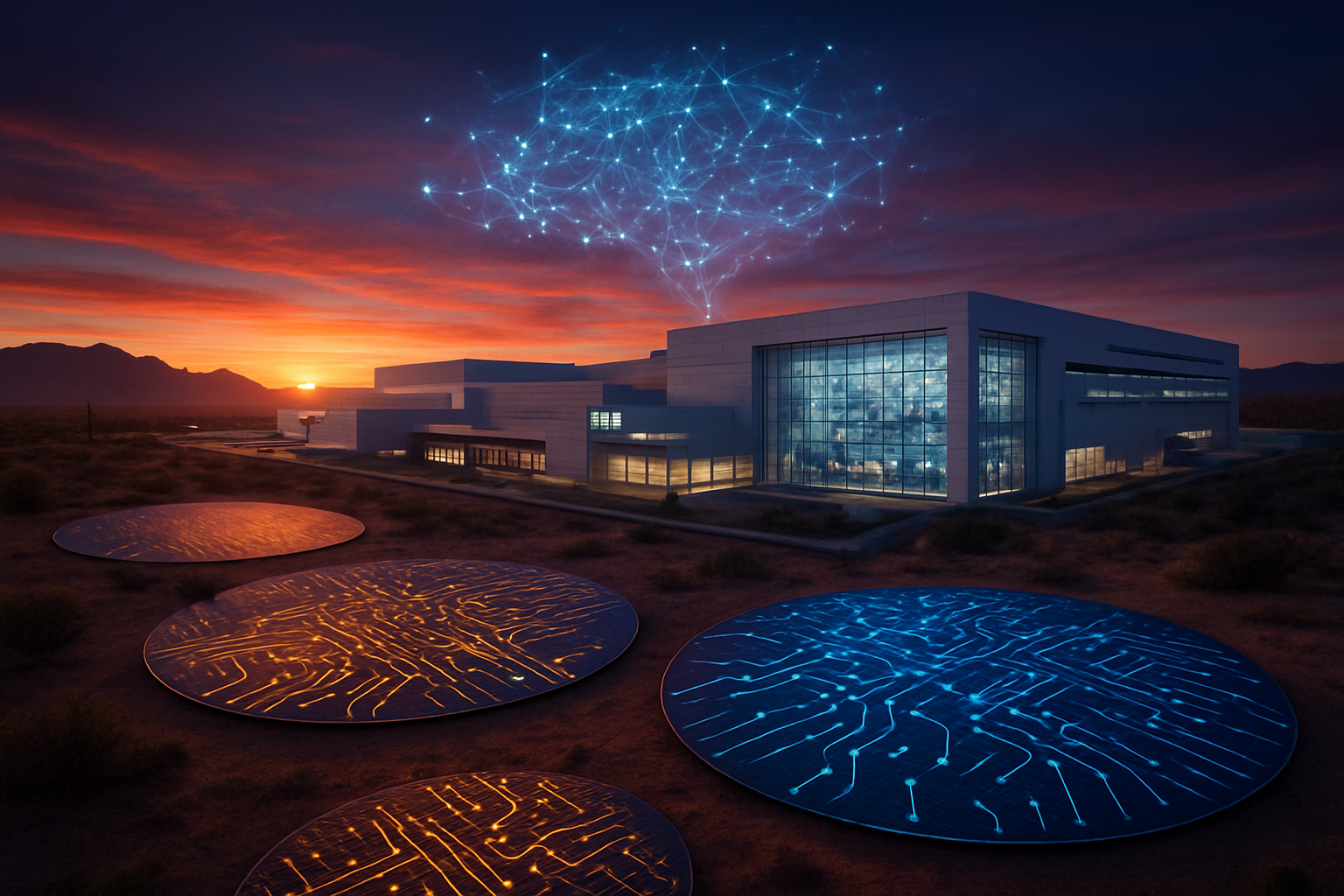
Tag: AI Hardware

  • The Great Decoupling: How Custom Silicon is Breaking NVIDIA’s Iron Grip on the AI Cloud

    The Great Decoupling: How Custom Silicon is Breaking NVIDIA’s Iron Grip on the AI Cloud

    As we close out 2025, the landscape of artificial intelligence infrastructure has undergone a seismic shift. For years, the industry’s reliance on NVIDIA Corp. (NASDAQ: NVDA) was absolute, with the company’s H100 and Blackwell GPUs serving as the undisputed currency of the AI revolution. However, the final months of 2025 have confirmed a new reality: the era of the "General Purpose GPU" monopoly is ending. Cloud hyperscalers—Alphabet Inc. (NASDAQ: GOOGL), Amazon.com Inc. (NASDAQ: AMZN), and Microsoft Corp. (NASDAQ: MSFT)—have successfully transitioned from being NVIDIA’s biggest customers to its most formidable competitors, deploying custom-built AI Application-Specific Integrated Circuits (ASICs) at a scale previously thought impossible.

    This transition is not merely about saving costs; it is a fundamental re-engineering of the AI stack. By bypassing traditional GPUs, these tech giants are gaining unprecedented control over their supply chains, energy consumption, and software ecosystems. With the recent launch of Google’s seventh-generation TPU, "Ironwood," and Amazon’s "Trainium3," the performance gap that once protected NVIDIA has all but vanished, ushering in a "Great Decoupling" that is redefining the economics of the cloud.

    The Technical Frontier: Ironwood, Trainium3, and the Push for 3nm

    The technical specifications of 2025’s custom silicon represent a quantum leap over the experimental chips of just two years ago. Google’s Ironwood (TPU v7), unveiled in late 2025, has become the new benchmark for scaling. Built on a cutting-edge 3nm process, Ironwood delivers a staggering 4.6 PetaFLOPS of FP8 performance per chip, narrowly edging out the standard NVIDIA Blackwell B200. What sets Ironwood apart is its "optical switching" fabric, which allows Google to link 9,216 chips into a single "Superpod" with 1.77 Petabytes of shared HBM3e memory. This architecture virtually eliminates the communication bottlenecks that plague traditional Ethernet-based GPU clusters, making it the preferred choice for training the next generation of trillion-parameter models.

    Amazon’s Trainium3, launched at re:Invent in December 2025, focuses on a different technical triumph: the "Total Cost of Ownership" (TCO). While its raw compute of 2.5 PetaFLOPS trails NVIDIA’s top-tier Blackwell Ultra, the Trainium3 UltraServer packs 144 chips into a single rack, delivering 0.36 ExaFLOPS of aggregate performance at a fraction of the power draw. Amazon’s dual-chiplet design allows for high yields and lower manufacturing costs, enabling AWS to offer AI training credits at prices 40% to 65% lower than equivalent NVIDIA-based instances.

    Microsoft, while facing some design hurdles with its Maia 200 (now expected in early 2026), has pivoted its technical strategy toward vertical integration. At Ignite 2025, Microsoft showcased the Azure Cobalt 200, a 3nm Arm-based CPU designed to work in tandem with the Azure Boost DPU (Data Processing Unit). This combination offloads networking and storage tasks from the AI accelerators, ensuring that even the current Maia 100 chips operate at near-peak theoretical utilization. This "system-level" approach differs from NVIDIA’s "chip-first" philosophy, focusing on how data moves through the entire data center rather than just the speed of a single processor.

    Market Disruption: The End of the "GPU Tax"

    The strategic implications of this shift are profound. For years, cloud providers were forced to pay what many called the "NVIDIA Tax"—massive premiums that resulted in 80% gross margins for the chipmaker. By 2025, the hyperscalers have reclaimed this margin. For Meta Platforms Inc. (NASDAQ: META), which recently began renting Google’s TPUs to supplement its own internal MTIA (Meta Training and Inference Accelerator) efforts, the move to custom silicon represents a multi-billion dollar saving in capital expenditure.

    This development has created a new competitive dynamic between major AI labs. Anthropic, backed heavily by Amazon and Google, now does the vast majority of its training on Trainium and TPU clusters. This gives them a significant cost advantage over OpenAI, which remains more closely tied to NVIDIA hardware via its partnership with Microsoft. However, even that is changing; Microsoft’s move to make its Azure Foundry "hardware agnostic" allows it to shift internal workloads like Microsoft 365 Copilot onto Maia silicon, freeing up its limited NVIDIA supply for high-paying external customers.

    Furthermore, the rise of custom ASICs is disrupting the startup ecosystem. New AI companies are no longer defaulting to CUDA (NVIDIA’s proprietary software platform). With the emergence of OpenXLA and PyTorch 2.5+, which provide seamless abstraction layers across different hardware types, the "software moat" that once protected NVIDIA is being drained. Amazon’s shocking announcement that its upcoming Trainium4 will natively support CUDA-compiled kernels is perhaps the final nail in the coffin for hardware lock-in, signaling a future where code can run on any silicon, anywhere.

    The Wider Significance: Power, Sovereignty, and Sustainability

    Beyond the corporate balance sheets, the rise of custom AI silicon addresses the most pressing crisis facing the tech industry: the power grid. As of late 2025, data centers are consuming an estimated 8% of total US electricity. Custom ASICs like Google’s Ironwood are designed with "inference-first" architectures that are up to 3x more energy-efficient than general-purpose GPUs. This efficiency is no longer a luxury; it is a requirement for obtaining building permits for new data centers in power-constrained regions like Northern Virginia and Dublin.

    This trend also reflects a broader move toward "Technological Sovereignty." During the supply chain crunches of 2023 and 2024, hyperscalers were "price takers," at the mercy of NVIDIA’s allocation schedules. In 2025, they are "price makers." By controlling the silicon design, Google, Amazon, and Microsoft can dictate their own roadmap, optimizing hardware for specific model architectures like Mixture-of-Experts (MoE) or State Space Models (SSM) that were not yet mainstream when NVIDIA’s Blackwell was first designed.

    However, this shift is not without concerns. The fragmentation of the hardware landscape could lead to a "two-tier" AI world: one where the "Big Three" cloud providers have access to hyper-efficient, low-cost custom silicon, while smaller cloud providers and sovereign nations are left competing for increasingly expensive, general-purpose GPUs. This could further centralize the power of AI development into the hands of a few trillion-dollar entities, raising antitrust questions that regulators in the US and EU are already beginning to probe as we head into 2026.

    The Horizon: Inference-First and the 2nm Race

    Looking ahead to 2026 and 2027, the focus of custom silicon is expected to shift from "Training" to "Massive-Scale Inference." As AI models become embedded in every aspect of computing—from operating systems to real-time video translation—the demand for chips that can run models cheaply and instantly will skyrocket. We expect to see "Edge-ASICs" from these hyperscalers that bridge the gap between the cloud and local devices, potentially challenging the dominance of Apple Inc. (NASDAQ: AAPL) in the AI-on-device space.

    The next major milestone will be the transition to 2nm process technology. Reports suggest that both Google and Amazon have already secured 2nm capacity at Taiwan Semiconductor Manufacturing Co. (NYSE: TSM) for 2026. These next-gen chips will likely integrate "Liquid-on-Chip" cooling technologies to manage the extreme heat densities of trillion-parameter processing. The challenge will remain software; while abstraction layers have improved, the "last mile" of optimization for custom silicon still requires specialized engineering talent that remains in short supply.

    A New Era of AI Infrastructure

    The rise of custom AI silicon marks the end of the "GPU Gold Rush" and the beginning of the "ASIC Integration" era. By late 2025, the hyperscalers have proven that they can not only match NVIDIA’s performance but exceed it in the areas that matter most: scale, cost, and efficiency. This development is perhaps the most significant in the history of AI hardware, as it breaks the bottleneck that threatened to stall AI progress due to high costs and limited supply.

    As we move into 2026, the industry will be watching closely to see how NVIDIA responds to this loss of market share. While NVIDIA remains the leader in raw innovation and software ecosystem depth, the "Great Decoupling" is now an irreversible reality. For enterprises and developers, this means more choice, lower costs, and a more resilient AI infrastructure. The AI revolution is no longer being fought on a single front; it is being won in the custom-built silicon foundries of the world’s largest cloud providers.


    This content is intended for informational purposes only and represents analysis of current AI developments.

    TokenRing AI delivers enterprise-grade solutions for multi-agent AI workflow orchestration, AI-powered development tools, and seamless remote collaboration platforms.
    For more information, visit https://www.tokenring.ai/.

  • Silicon Sovereignty: China’s Strategic Pivot to RISC-V Accelerates Amid US Tech Blockades

    Silicon Sovereignty: China’s Strategic Pivot to RISC-V Accelerates Amid US Tech Blockades

    As of late 2025, the global semiconductor landscape has reached a definitive tipping point. Driven by increasingly stringent US export controls that have severed access to high-end proprietary architectures, China has executed a massive, state-backed migration to RISC-V. This open-standard instruction set architecture (ISA) has transformed from a niche academic project into the backbone of China’s "Silicon Sovereignty" strategy, providing a critical loophole in the Western containment of Chinese AI and high-performance computing.

    The immediate significance of this shift cannot be overstated. By leveraging RISC-V, Chinese tech giants are no longer beholden to the licensing whims of Western firms or the jurisdictional reach of US export laws. This pivot has not only insulated the Chinese domestic market from further sanctions but has also sparked a rapid evolution in AI hardware design, where hardware-software co-optimization is now being used to bridge the performance gap left by the absence of top-tier Western GPUs.

    Technical Milestones and the Rise of High-Performance RISC-V

    The technical maturation of RISC-V in 2025 is headlined by Alibaba (NYSE: BABA) and its chip-design subsidiary, T-Head. In March 2025, the company unveiled the XuanTie C930, a server-grade 64-bit multi-core processor that represents a quantum leap for the architecture. Unlike its predecessors, the C930 is fully compatible with the RVA23 profile and features dual 512-bit vector units and an integrated 8 TOPS Matrix engine specifically designed for AI workloads. This allows the chip to compete directly with mid-range server offerings from Intel (NASDAQ: INTC) and Advanced Micro Devices (NASDAQ: AMD), achieving performance levels previously thought impossible for an open-source ISA.

    Parallel to private sector efforts, the Chinese Academy of Sciences (CAS) has reached a major milestone with Project XiangShan. The 2025 release of the "Kunminghu" architecture—often described as the "Linux of processors"—targets clock speeds of 3GHz. The Kunminghu core is designed to match the performance of the ARM (NASDAQ: ARM) Neoverse N2, providing a high-performance, royalty-free alternative for data centers and cloud infrastructure. This development is crucial because it proves that open-source hardware can achieve the same IPC (instructions per cycle) efficiency as the most advanced proprietary designs.

    What sets this new generation of RISC-V chips apart is their native support for emerging AI data formats. Following the breakthrough success of models like DeepSeek-V3 earlier this year, Chinese designers have integrated support for formats like UE8M0 FP8 directly into the silicon. This level of hardware-software synergy allows for highly efficient AI inference on domestic hardware, effectively bypassing the need for restricted NVIDIA (NASDAQ: NVDA) H100 or H200 accelerators. Industry experts have noted that while individual RISC-V cores may still lag behind the absolute peak of US silicon, the ability to customize instructions for specific AI kernels gives Chinese firms a unique "tailor-made" advantage.

    Initial reactions from the global research community have been a mix of awe and anxiety. While proponents of open-source technology celebrate the rapid advancement of the RISC-V ecosystem, industry analysts warn that the fragmentation of the hardware world is accelerating. The move of RISC-V International to Switzerland in 2020 has proven to be a masterstroke of jurisdictional engineering, ensuring that the core specifications remain beyond the reach of the US Department of Commerce, even as Chinese contributions to the standard now account for nearly 50% of the organization’s premier membership.

    Disrupting the Global Semiconductor Hierarchy

    The strategic expansion of RISC-V is sending shockwaves through the established tech hierarchy. ARM Holdings (NASDAQ: ARM) is perhaps the most vulnerable, as its primary revenue engine—licensing high-performance IP—is being directly cannibalized in one of its largest markets. With the US tightening controls on ARM’s Neoverse V-series cores due to their US-origin technology, Chinese firms like Tencent (HKG: 0700) and Baidu (NASDAQ: BIDU) are shifting their cloud-native development to RISC-V to ensure long-term supply chain security. This represents a permanent loss of market share for Western IP providers that may never be recovered.

    For the "Big Three" of US silicon—NVIDIA (NASDAQ: NVDA), Intel (NASDAQ: INTC), and AMD (NASDAQ: AMD)—the rise of RISC-V creates a two-front challenge. First, it accelerates the development of domestic Chinese AI accelerators that serve as "good enough" substitutes for export-restricted GPUs. Second, it creates a competitive pressure in the Internet of Things (IoT) and automotive sectors, where RISC-V’s modularity and lack of licensing fees make it an incredibly attractive option for global manufacturers. Companies like Qualcomm (NASDAQ: QCOM) and Western Digital (NASDAQ: WDC) are now forced to balance their participation in the open RISC-V ecosystem with the shifting political landscape in Washington.

    The disruption extends beyond hardware to the entire software stack. The aggressive optimization of the openEuler and OpenHarmony operating systems for RISC-V architecture has created a robust domestic ecosystem. As Chinese tech giants migrate their LLMs, such as Baidu’s Ernie Bot, to run on massive RISC-V clusters, the strategic advantage once held by NVIDIA’s CUDA platform is being challenged by a "software-defined hardware" approach. This allows Chinese startups to innovate at the compiler and kernel levels, potentially creating a parallel AI economy that is entirely independent of Western proprietary standards.

    Market positioning is also shifting as RISC-V becomes a symbol of "neutral" technology for the Global South. By championing an open standard, China is positioning itself as a leader in a more democratic hardware landscape, contrasting its approach with the "walled gardens" of US tech. This has significant implications for market expansion in regions like Southeast Asia and the Middle East, where countries are increasingly wary of becoming collateral damage in the US-China tech war and are seeking hardware platforms that cannot be deactivated by a foreign power.

    Geopolitics and the "Open-Source Loophole"

    The wider significance of China’s RISC-V surge lies in its challenge to the effectiveness of modern export controls. For decades, the US has controlled the tech landscape by bottlenecking key proprietary technologies. However, RISC-V represents a new paradigm: a globally collaborative, open-source standard that no single nation can truly "own" or restrict. This has led to a heated debate in Washington over the so-called "open-source loophole," where lawmakers argue that US participation in RISC-V International is inadvertently providing China with the blueprints for advanced military and AI capabilities.

    This development fits into a broader trend of "technological decoupling," where the world is splitting into two distinct hardware and software ecosystems—a "splinternet" of silicon. The concern among global tech leaders is that if the US moves to sanction the RISC-V standard itself, it would destroy the very concept of open-source collaboration, forcing a total fracture of the global semiconductor industry. Such a move would likely backfire, as it would isolate US companies from the rapid innovations occurring within the Chinese RISC-V community while failing to stop China’s progress.

    Comparisons are being drawn to previous milestones like the rise of Linux in the 1990s. Just as Linux broke the monopoly of proprietary operating systems, RISC-V is poised to break the duopoly of x86 and ARM. However, the stakes are significantly higher in 2025, as the architecture is being used to power the next generation of autonomous weapons, surveillance systems, and frontier AI models. The tension between the benefits of open innovation and the requirements of national security has never been more acute.

    Furthermore, the environmental and economic impacts of this shift are starting to emerge. RISC-V’s modular nature allows for more energy-efficient, application-specific designs. As China builds out massive "Green AI" data centers powered by custom RISC-V silicon, the global industry may be forced to adopt these open standards simply to remain competitive in power efficiency. The irony is that US export controls, intended to slow China down, may have instead forced the creation of a leaner, more efficient, and more resilient Chinese tech sector.

    The Horizon: SAFE Act and the Future of Open Silicon

    Looking ahead, the primary challenge for the RISC-V ecosystem will be the legislative response from the West. In December 2025, the US introduced the Secure and Feasible Export of Chips (SAFE) Act, which specifically targets high-performance extensions to the RISC-V standard. If passed, the act could restrict US companies from contributing advanced vector or matrix-multiplication instructions to the global standard if those contributions are deemed to benefit "adversary" nations. This could lead to a "forking" of the RISC-V ISA, with one version used in the West and another, more AI-optimized version developed in China.

    In the near term, expect to see the first wave of RISC-V-powered consumer laptops and high-end automotive cockpits hitting the Chinese market. These devices will serve as a proof-of-concept for the architecture’s versatility beyond the data center. The long-term goal for Chinese planners is clear: total vertical integration. From the instruction set up to the application layer, China aims to eliminate every single point of failure that could be exploited by foreign sanctions. The success of this endeavor depends on whether the global developer community continues to support RISC-V as a neutral, universal standard.

    Experts predict that the next major battleground will be the "software gap." While the hardware is catching up, the maturity of libraries, debuggers, and optimization tools for RISC-V still lags behind ARM and x86. However, with thousands of Chinese engineers now dedicated to the RISC-V ecosystem, this gap is closing faster than anticipated. The next 12 to 18 months will be critical in determining if RISC-V can achieve the "critical mass" necessary to become the world’s third major computing platform, potentially relegated only by the severity of future geopolitical interventions.

    A New Era of Global Computing

    The strategic expansion of RISC-V in China marks a definitive chapter in AI history. What began as an academic exercise at UC Berkeley has become the centerpiece of a geopolitical struggle for technological dominance. China’s successful pivot to RISC-V demonstrates that in an era of global connectivity, proprietary blockades are increasingly difficult to maintain. The development of the XuanTie C930 and the XiangShan project are not just technical achievements; they are declarations of independence from a Western-centric hardware order.

    The key takeaway for the industry is that the "open-source genie" is out of the bottle. Efforts to restrict RISC-V may only serve to accelerate its development in regions outside of US control, ultimately weakening the influence of American technology standards. As we move into 2026, the significance of this development will be measured by how many other nations follow China’s lead in adopting RISC-V to safeguard their own digital futures.

    In the coming weeks and months, all eyes will be on the US Congress and the final language of the SAFE Act. Simultaneously, the industry will be watching for the first benchmarks of DeepSeek’s next-generation models running natively on RISC-V clusters. These results will tell us whether the "Silicon Sovereignty" China seeks is a distant dream or a present reality. The era of the proprietary hardware monopoly is ending, and the age of open silicon has truly begun.


    This content is intended for informational purposes only and represents analysis of current AI developments.

    TokenRing AI delivers enterprise-grade solutions for multi-agent AI workflow orchestration, AI-powered development tools, and seamless remote collaboration platforms.
    For more information, visit https://www.tokenring.ai/.

  • Beyond the Chip: Nvidia’s Rubin Architecture Ushers in the Era of the Gigascale AI Factory

    Beyond the Chip: Nvidia’s Rubin Architecture Ushers in the Era of the Gigascale AI Factory

    As 2025 draws to a close, the semiconductor landscape is bracing for its most significant transformation yet. NVIDIA (NASDAQ: NVDA) has officially moved into the sampling phase for its highly anticipated Rubin architecture, the successor to the record-breaking Blackwell generation. While Blackwell focused on scaling the GPU to its physical limits, Rubin represents a fundamental pivot in silicon engineering: the transition from individual accelerators to "AI Factories"—massive, multi-die systems designed to treat an entire data center as a single, unified computer.

    This shift comes at a critical juncture as the industry moves toward "Agentic AI" and million-token context windows. The Rubin platform is not merely a faster processor; it is a holistic re-architecting of compute, memory, and networking. By integrating next-generation HBM4 memory and the new Vera CPU, Nvidia is positioning itself to maintain its near-monopoly on high-end AI infrastructure, even as competitors and cloud providers attempt to internalize their chip designs.

    The Technical Blueprint: R100, Vera, and the HBM4 Revolution

    At the heart of the Rubin platform is the R100 GPU, a marvel of 3nm engineering manufactured by Taiwan Semiconductor Manufacturing Company (NYSE: TSM). Unlike previous generations that pushed the limits of a single reticle, the R100 utilizes a sophisticated multi-die design enabled by TSMC’s CoWoS-L packaging. Each R100 package consists of two primary compute dies and dedicated I/O tiles, effectively doubling the silicon area available for logic. This allows a single Rubin package to deliver an astounding 50 PFLOPS of FP4 precision compute, roughly 2.5 times the performance of a Blackwell GPU.

    Complementing the GPU is the Vera CPU, Nvidia’s successor to the Grace processor. Vera features 88 custom Arm-based cores designed specifically for AI orchestration and data pre-processing. The interconnect between the CPU and GPU has been upgraded to NVLink-C2C, providing a staggering 1.8 TB/s of bandwidth. Perhaps most significant is the debut of HBM4 (High Bandwidth Memory 4). Supplied by partners like SK Hynix (KRX: 000660) and Micron (NASDAQ: MU), the Rubin GPU features 288GB of HBM4 capacity with a bandwidth of 13.5 TB/s, a necessity for the trillion-parameter models expected to dominate 2026.

    Beyond raw power, Nvidia has introduced a specialized component called the Rubin CPX. This "Context Accelerator" is designed specifically for the prefill stage of large language model (LLM) inference. By using high-speed GDDR7 memory and specialized hardware for attention mechanisms, the CPX addresses the "memory wall" that often bottlenecks long-context window tasks, such as analyzing entire codebases or hour-long video files.

    Market Dominance and the Competitive Moat

    The move to the Rubin architecture solidifies Nvidia’s strategic advantage over rivals like AMD (NASDAQ: AMD) and Intel (NASDAQ: INTC). By moving to an annual release cadence and a "system-level" product, Nvidia is forcing competitors to compete not just with a chip, but with an entire rack-scale ecosystem. The Vera Rubin NVL144 system, which integrates 144 GPU dies and 36 Vera CPUs into a single liquid-cooled rack, is designed to be the "unit of compute" for the next generation of cloud infrastructure.

    Major cloud service providers (CSPs) including Amazon (NASDAQ: AMZN), Microsoft (NASDAQ: MSFT), and Alphabet (NASDAQ: GOOGL) are already lining up for early Rubin shipments. While these companies have developed their own internal AI chips (such as Trainium and TPU), the sheer software ecosystem of Nvidia’s CUDA, combined with the interconnect performance of NVLink 6, makes Rubin the indispensable choice for frontier model training. This puts pressure on secondary hardware players, as the barrier to entry is no longer just silicon performance, but the ability to provide a multi-terabit networking fabric that can scale to millions of interconnected units.

    Scaling the AI Factory: Implications for the Global Landscape

    The Rubin architecture marks the official arrival of the "AI Factory" era. Nvidia’s vision is to transform the data center from a collection of servers into a production line for intelligence. This has profound implications for global energy consumption and infrastructure. A single NVL576 Rubin Ultra rack is expected to draw upwards of 600kW of power, requiring advanced 800V DC power delivery and sophisticated liquid-to-liquid cooling systems. This shift is driving a secondary boom in the industrial cooling and power management sectors.

    Furthermore, the Rubin generation highlights the growing importance of silicon photonics. To bridge the gap between racks without the latency of traditional copper wiring, Nvidia is integrating optical interconnects directly into its X1600 switches. This "Giga-scale" networking allows a cluster of 100,000 GPUs to behave as if they were on a single circuit board. While this enables unprecedented AI breakthroughs, it also raises concerns about the centralization of AI power, as only a handful of nations and corporations can afford the multi-billion-dollar price tag of a Rubin-powered factory.

    The Horizon: Rubin Ultra and the Path to AGI

    Looking ahead to 2026 and 2027, Nvidia has already teased the Rubin Ultra variant. This iteration is expected to push memory capacities toward 1TB per GPU package using 16-high HBM4e stacks. The industry predicts that this level of memory density will be the catalyst for "World Models"—AI systems capable of simulating complex physical environments in real-time for robotics and autonomous vehicles.

    The primary challenge facing the Rubin rollout remains the supply chain. The reliance on TSMC’s advanced 3nm nodes and the high-precision assembly required for CoWoS-L packaging means that supply will likely remain constrained throughout 2026. Experts also point to the "software tax," where the complexity of managing a multi-die, rack-scale system requires a new generation of orchestration software that can handle hardware failures and data sharding at an unprecedented scale.

    A New Benchmark for Artificial Intelligence

    The Rubin architecture is more than a generational leap; it is a statement of intent. By moving to a multi-die, system-centric model, Nvidia has effectively redefined what it means to build AI hardware. The integration of the Vera CPU, HBM4, and NVLink 6 creates a vertically integrated powerhouse that will likely define the state-of-the-art for the next several years.

    As we move into 2026, the industry will be watching the first deployments of the Vera Rubin NVL144 systems. If these "AI Factories" deliver on their promise of 2.5x performance gains and seamless long-context processing, the path toward Artificial General Intelligence (AGI) may be paved with Nvidia silicon. For now, the tech world remains in a state of high anticipation, as the first Rubin samples begin to land in the labs of the world’s leading AI researchers.


    This content is intended for informational purposes only and represents analysis of current AI developments.

    TokenRing AI delivers enterprise-grade solutions for multi-agent AI workflow orchestration, AI-powered development tools, and seamless remote collaboration platforms.
    For more information, visit https://www.tokenring.ai/.

  • The 2048-Bit Revolution: How the Shift to HBM4 in 2025 is Shattering AI’s Memory Wall

    The 2048-Bit Revolution: How the Shift to HBM4 in 2025 is Shattering AI’s Memory Wall

    As the calendar turns to late 2025, the artificial intelligence industry is standing at the precipice of its most significant hardware transition since the dawn of the generative AI boom. The arrival of High-Bandwidth Memory Generation 4 (HBM4) marks a fundamental redesign of how data moves between storage and processing units. For years, the "memory wall"—the bottleneck where processor speeds outpaced the ability of memory to deliver data—has been the primary constraint for scaling large language models (LLMs). With the mass production of HBM4 slated for the coming months, that wall is finally being dismantled.

    The immediate significance of this shift cannot be overstated. Leading semiconductor giants are not just increasing clock speeds; they are doubling the physical width of the data highway. By moving from the long-standing 1024-bit interface to a massive 2048-bit interface, the industry is enabling a new class of AI accelerators that can handle the trillion-parameter models of the future. This transition is expected to deliver a staggering 40% improvement in power efficiency and a nearly 20% boost in raw AI training performance, providing the necessary fuel for the next generation of "agentic" AI systems.

    The Technical Leap: Doubling the Data Highway

    The defining technical characteristic of HBM4 is the doubling of the I/O interface from 1024-bit—a standard that has persisted since the first generation of HBM—to 2048-bit. This "wider bus" approach allows for significantly higher bandwidth without requiring the extreme, heat-generating pin speeds that would be necessary to achieve similar gains on narrower interfaces. Current specifications for HBM4 target bandwidths exceeding 2.0 TB/s per stack, with some manufacturers like Micron Technology (NASDAQ: MU) aiming for as high as 2.8 TB/s.

    Beyond the interface width, HBM4 introduces a radical change in how memory stacks are built. For the first time, the "base die"—the logic layer at the bottom of the memory stack—is being manufactured using advanced foundry logic processes (such as 5nm and 12nm) rather than traditional memory processes. This shift has necessitated unprecedented collaborations, such as the "one-team" alliance between SK Hynix (KRX: 000660) and Taiwan Semiconductor Manufacturing Company (NYSE: TSM). By using a logic-based base die, manufacturers can integrate custom features directly into the memory, effectively turning the HBM stack into a semi-compute-capable unit.

    This architectural shift differs from previous generations like HBM3e, which focused primarily on incremental speed increases and layer stacking. HBM4 supports up to 16-high stacks, enabling capacities of 48GB to 64GB per stack. This means a single GPU equipped with six HBM4 stacks could boast nearly 400GB of ultra-fast VRAM. Initial reactions from the AI research community have been electric, with engineers at major labs noting that HBM4 will allow for larger "context windows" and more complex multi-modal reasoning that was previously constrained by memory capacity and latency.

    Competitive Implications: The Race for HBM Dominance

    The shift to HBM4 has rearranged the competitive landscape of the semiconductor industry. SK Hynix, the current market leader, has successfully pulled its HBM4 roadmap forward to late 2025, maintaining its lead through its proprietary Advanced MR-MUF (Mass Reflow Molded Underfill) technology. However, Samsung Electronics (KRX: 005930) is mounting a massive counter-offensive. In a historic move, Samsung has partnered with its traditional foundry rival, TSMC, to ensure its HBM4 stacks are compatible with the industry-standard CoWoS (Chip-on-Wafer-on-Substrate) packaging used by NVIDIA (NASDAQ: NVDA).

    For AI giants like NVIDIA and Advanced Micro Devices (NASDAQ: AMD), HBM4 is the cornerstone of their 2026 product cycles. NVIDIA’s upcoming "Rubin" architecture is designed specifically to leverage the 2048-bit interface, with projections suggesting a 3.3x increase in training performance over the current Blackwell generation. This development solidifies the strategic advantage of companies that can secure HBM4 supply. Reports indicate that the entire production capacity for HBM4 through 2026 is already "sold out," with hyperscalers like Google, Amazon, and Meta placing massive pre-orders to ensure their future AI clusters aren't left in the slow lane.

    Startups and smaller AI labs may find themselves at a disadvantage during this transition. The increased complexity of HBM4 is expected to drive prices up by as much as 50% compared to HBM3e. This "premiumization" of memory could widen the gap between the "compute-rich" tech giants and the rest of the industry, as the cost of building state-of-the-art AI clusters continues to skyrocket. Market analysts suggest that HBM4 will account for over 50% of all HBM revenue by 2027, making it the most lucrative segment of the memory market.

    Wider Significance: Powering the Age of Agentic AI

    The transition to HBM4 fits into a broader trend of "custom silicon" for AI. We are moving away from general-purpose hardware toward highly specialized systems where memory and logic are increasingly intertwined. The 40% improvement in power-per-bit efficiency is perhaps the most critical metric for the broader landscape. As global data centers face mounting pressure over energy consumption, the ability of HBM4 to deliver more "tokens per watt" is essential for the sustainable scaling of AI.

    Comparing this to previous milestones, the shift to HBM4 is akin to the transition from mechanical hard drives to SSDs in terms of its impact on system responsiveness. It addresses the "Memory Wall" not just by making the wall thinner, but by fundamentally changing how the processor interacts with data. This enables the training of models with tens of trillions of parameters, moving us closer to Artificial General Intelligence (AGI) by allowing models to maintain more information in "active memory" during complex tasks.

    However, the move to HBM4 also raises concerns about supply chain fragility. The deep integration between memory makers and foundries like TSMC creates a highly centralized ecosystem. Any geopolitical or logistical disruption in the Taiwan Strait or South Korea could now bring the entire global AI industry to a standstill. This has prompted increased interest in "sovereign AI" initiatives, with countries looking to secure their own domestic pipelines for high-end memory and logic manufacturing.

    Future Horizons: Beyond the Interposer

    Looking ahead, the innovations introduced with HBM4 are paving the way for even more radical designs. Experts predict that the next step will be "Direct 3D Stacking," where memory stacks are bonded directly on top of the GPU or CPU without the need for a silicon interposer. This would further reduce latency and physical footprint, potentially allowing for powerful AI capabilities to migrate from massive data centers to "edge" devices like high-end workstations and autonomous vehicles.

    In the near term, we can expect the announcement of "HBM4e" (Extended) by late 2026, which will likely push capacities toward 100GB per stack. The challenge that remains is thermal management; as stacks get taller and denser, dissipating the heat from the center of the memory stack becomes an engineering nightmare. Solutions like liquid cooling and new thermal interface materials are already being researched to address these bottlenecks.

    What experts predict next is the "commoditization of custom logic." As HBM4 allows customers to put their own logic into the base die, we may see companies like OpenAI or Anthropic designing their own proprietary memory controllers to optimize how their specific models access data. This would represent the final step in the vertical integration of the AI stack.

    Wrapping Up: A New Era of Compute

    The shift to HBM4 in 2025 represents a watershed moment for the technology industry. By doubling the interface width and embracing a logic-based architecture, memory manufacturers have provided the necessary infrastructure for the next great leap in AI capability. The "Memory Wall" that once threatened to stall the AI revolution is being replaced by a 2048-bit gateway to unprecedented performance.

    The significance of this development in AI history will likely be viewed as the moment hardware finally caught up to the ambitions of software. As we watch the first HBM4-equipped accelerators roll off the production lines in the coming months, the focus will shift from "how much data can we store" to "how fast can we use it." The "super-cycle" of AI infrastructure is far from over; in fact, with HBM4, it is just finding its second wind.

    In the coming weeks, keep a close eye on the final JEDEC standardization announcements and the first performance benchmarks from early Rubin GPU samples. These will be the definitive indicators of just how fast the AI world is about to move.


    This content is intended for informational purposes only and represents analysis of current AI developments.

    TokenRing AI delivers enterprise-grade solutions for multi-agent AI workflow orchestration, AI-powered development tools, and seamless remote collaboration platforms.
    For more information, visit https://www.tokenring.ai/.

  • The Angstrom Era Arrives: Intel and ASML Solidify Lead in High-NA EUV Commercialization

    The Angstrom Era Arrives: Intel and ASML Solidify Lead in High-NA EUV Commercialization

    As of December 18, 2025, the semiconductor industry has reached a historic inflection point. Intel Corporation (NASDAQ: INTC) has officially confirmed the successful acceptance testing and validation of the ASML Holding N.V. (NASDAQ: ASML) Twinscan EXE:5200B, the world’s first high-volume production High-NA Extreme Ultraviolet (EUV) lithography system. This milestone signals the formal beginning of the "Angstrom Era" for commercial silicon, as Intel moves its 14A (1.4nm-class) process node into the final stages of pre-production readiness.

    The partnership between Intel and ASML represents a multi-billion dollar gamble that is now beginning to pay dividends. By becoming the first mover in High-NA technology, Intel aims to reclaim its "process leadership" crown, which it lost to rivals over the last decade. The immediate significance of this development cannot be overstated: it provides the physical foundation for the next generation of AI accelerators and high-performance computing (HPC) chips that will power the increasingly complex Large Language Models (LLMs) of the late 2020s.

    Technical Mastery: 0.55 NA and the End of Multi-Patterning

    The transition from standard (Low-NA) EUV to High-NA EUV is the most significant leap in lithography in over twenty years. At the heart of this shift is the increase in the Numerical Aperture (NA) from 0.33 to 0.55. This change allows for a 1.7x increase in resolution, enabling the printing of features so small they are measured in Angstroms rather than nanometers. While standard EUV tools had begun to hit a physical limit, requiring "double-patterning" or even "quad-patterning" to achieve 2nm-class densities, the EXE:5200B allows Intel to print these critical layers in a single pass.

    Technically, the EXE:5200B is a marvel of engineering, capable of a throughput of 175 to 200 wafers per hour. It features an overlay accuracy of 0.7nm, a precision level necessary to align the dozens of microscopic layers that comprise a modern 1.4nm transistor. This reduction in patterning complexity is not just a matter of elegance; it drastically reduces manufacturing cycle times and eliminates the "stochastic" defects that often plague multi-patterning processes. Initial data from Intel’s D1X facility in Oregon suggests that the 14A node is already showing superior yield curves compared to the previous 18A node at a similar point in its development cycle.

    The industry’s reaction has been one of cautious awe. While skeptics initially pointed to the $400 million price tag per machine as a potential financial burden, the technical community has praised Intel’s "stitching" techniques. Because High-NA tools have a smaller exposure field—effectively half the size of standard EUV—Intel had to develop proprietary software and hardware solutions to "stitch" two halves of a chip design together seamlessly. By late 2025, these techniques have been proven stable, clearing the path for the mass production of massive AI "super-chips" that exceed traditional reticle limits.

    Shifting the Competitive Chessboard

    The commercialization of High-NA EUV has created a stark divergence in the strategies of the world’s leading foundries. While Intel has gone "all-in" on the new tools, Taiwan Semiconductor Manufacturing Company (NYSE: TSM), or TSMC, has taken a more conservative path. TSMC’s A14 node, scheduled for a similar timeframe, continues to rely on Low-NA EUV with advanced multi-patterning. TSMC’s leadership has argued that the cost-per-transistor remains lower with mature tools, but Intel’s early adoption of High-NA has effectively built a two-year "operational moat" in managing the complex optics and photoresist chemistries required for the 1.4nm era.

    This strategic lead is already attracting "AI-first" fabless companies. With the release of the Intel 14A PDK 0.5 (Process Design Kit) in late 2025, several major cloud service providers and AI chip startups have reportedly begun exploring Intel Foundry as a secondary or even primary source for their 2027 silicon. The ability to achieve 15% better performance-per-watt and a 20% increase in transistor density over 18A-P makes the 14A node an attractive target for those building the hardware for "Agentic AI" and trillion-parameter models.

    Samsung Electronics (KRX: 005930) finds itself in the middle ground, having recently received its first EXE:5200B modules to support its SF1.4 process. However, Intel’s head start in the Hillsboro R&D center means that Intel engineers have already spent two years "learning" the quirks of the High-NA light source and anamorphic lenses. This experience is critical; in the semiconductor world, knowing how to fix a tool when it goes down is as important as owning the tool itself. Intel’s deep integration with ASML has essentially turned the Oregon D1X fab into a co-development site for the future of lithography.

    The Broader Significance for the AI Revolution

    The move to High-NA EUV is not merely a corporate milestone; it is a vital necessity for the continued survival of Moore’s Law. As AI models grow in complexity, the demand for "compute density"—the amount of processing power packed into a square millimeter of silicon—has become the primary bottleneck for the industry. The 14A node represents the first time the industry has moved beyond the "nanometer" nomenclature into the "Angstrom" era, providing the physical density required to keep pace with the exponential growth of AI training requirements.

    This development also has significant geopolitical implications. The successful commercialization of High-NA tools within the United States (at Intel’s Oregon and upcoming Ohio sites) strengthens the domestic semiconductor supply chain. As AI becomes a core component of national security and economic infrastructure, the ability to manufacture the world’s most advanced chips on home soil using the latest lithography techniques is a major strategic advantage for the Western tech ecosystem.

    However, the transition is not without its concerns. The extreme cost of High-NA tools could lead to a further consolidation of the semiconductor industry, as only a handful of companies can afford the $400 million-per-machine entry fee. This "billionaire’s club" of chipmaking risks creating a monopoly on the most advanced AI hardware, potentially slowing down innovation in smaller labs that cannot afford the premium for 1.4nm wafers. Comparisons are already being drawn to the early days of EUV, where the high barrier to entry eventually forced several players out of the leading-edge race.

    The Road to 10A and Beyond

    Looking ahead, the roadmap for High-NA EUV is already extending into the next decade. Intel has already hinted at its "10A" node (1.0nm), which will likely utilize even more advanced versions of the High-NA platform. Experts predict that by 2028, the use of High-NA will expand beyond just the most critical metal layers to include a majority of the chip’s structure, further simplifying the manufacturing flow. We are also seeing the horizon for "Hyper-NA" lithography, which ASML is currently researching to push beyond the 0.75 NA mark in the 2030s.

    In the near term, the challenge for Intel and ASML will be scaling this technology from a few machines in Oregon to dozens of machines across Intel’s global "Smart Capital" network, including Fabs 52 and 62 in Arizona. Maintaining high yields while operating these incredibly sensitive machines in a high-volume environment will be the ultimate test of the partnership. Furthermore, the industry must develop new "High-NA ready" photoresists and masks that can withstand the higher energy density of the focused EUV light without degrading.

    A New Chapter in Computing History

    The successful acceptance of the ASML Twinscan EXE:5200B by Intel marks the end of the experimental phase for High-NA EUV and the beginning of its commercial life. It is a moment that will likely be remembered as the point when Intel reclaimed its technical momentum and redefined the limits of what is possible in silicon. The 14A node is more than just a process update; it is a statement of intent that the Angstrom era is here, and it is powered by the closest collaboration between a toolmaker and a manufacturer in the history of the industry.

    As we look toward 2026 and 2027, the focus will shift from tool installation to "wafer starts." The industry will be watching closely to see if Intel can translate its technical lead into market share gains against TSMC. For now, the message is clear: the path to the future of AI and high-performance computing runs through the High-NA lenses of ASML and the cleanrooms of Intel. The next eighteen months will be critical as the first 14A test chips begin to emerge, offering a glimpse into the hardware that will define the next decade of artificial intelligence.


    This content is intended for informational purposes only and represents analysis of current AI developments.

    TokenRing AI delivers enterprise-grade solutions for multi-agent AI workflow orchestration, AI-powered development tools, and seamless remote collaboration platforms.
    For more information, visit https://www.tokenring.ai/.

  • Beyond Silicon: A Materials Science Revolution Reshaping the Future of Chip Design

    Beyond Silicon: A Materials Science Revolution Reshaping the Future of Chip Design

    The relentless march of technological progress, particularly in artificial intelligence (AI), 5G/6G communication, electric vehicles, and the burgeoning Internet of Things (IoT), is pushing the very limits of traditional silicon-based electronics. As Moore's Law, which has guided the semiconductor industry for decades, begins to falter, a quiet yet profound revolution in materials science is taking center stage. New materials, with their extraordinary electrical, thermal, and mechanical properties, are not merely incremental improvements; they are fundamentally redefining what's possible in chip design, promising a future of faster, smaller, more energy-efficient, and functionally diverse electronic devices. This shift is critical for sustaining the pace of innovation, addressing the escalating demands of modern computing, and overcoming the inherent physical and economic constraints that silicon now presents.

    The immediate significance of this materials science revolution is multifaceted. It promises continued miniaturization and unprecedented performance enhancements, enabling denser and more powerful chips than ever before. Critically, many of these novel materials inherently consume less power and generate less heat, directly addressing the critical need for extended battery life in mobile devices and substantial energy reductions in vast data centers. Beyond traditional computing metrics, these materials are unlocking entirely new functionalities, from flexible electronics and advanced sensors to neuromorphic computing architectures and robust high-frequency communication systems, laying the groundwork for the next generation of intelligent technologies.

    The Atomic Edge: Unpacking the Technical Revolution in Chip Materials

    The core of this revolution lies in the unique properties of several advanced materials that are poised to surpass silicon in specific applications. These innovations are directly tackling silicon's limitations, such as quantum tunneling, increased leakage currents, and difficulties in maintaining gate control at sub-5nm scales.

    Wide Bandgap (WBG) Semiconductors, notably Gallium Nitride (GaN) and Silicon Carbide (SiC), stand out for their superior electrical efficiency, heat resistance, higher breakdown voltages, and improved thermal stability. GaN, with its high electron mobility, is proving indispensable for fast switching in telecommunications, radar systems, 5G base stations, and rapid-charging technologies. SiC excels in high-power applications for electric vehicles, renewable energy systems, and industrial machinery due to its robust performance at elevated voltages and temperatures, offering significantly reduced energy losses compared to silicon.

    Two-Dimensional (2D) Materials represent a paradigm shift in miniaturization. Graphene, a single layer of carbon atoms, boasts exceptional electrical conductivity, strength, and ultra-high electron mobility, allowing for electricity conduction at higher speeds with minimal heat generation. This makes it a strong candidate for ultra-high-speed transistors, flexible electronics, and advanced sensors. Other 2D materials like Transition Metal Dichalcogenides (TMDs) such as molybdenum disulfide, and hexagonal boron nitride, enable atomic-thin channel transistors and monolithic 3D integration. Their tunable bandgaps and high thermal conductivity make them suitable for next-generation transistors, flexible displays, and even foundational elements for quantum computing. These materials allow for device scaling far beyond silicon's physical limits, addressing the fundamental challenges of miniaturization.

    Ferroelectric Materials are introducing a new era of memory and logic. These materials are non-volatile, operate at low power, and offer fast switching capabilities with high endurance. Their integration into Ferroelectric Random Access Memory (FeRAM) and Ferroelectric Field-Effect Transistors (FeFETs) provides energy-efficient memory and logic devices crucial for AI chips and neuromorphic computing, which demand efficient data storage and processing close to the compute units.

    Furthermore, III-V Semiconductors like Gallium Arsenide (GaAs) and Indium Phosphide (InP) are vital for optoelectronics and high-frequency applications. Unlike silicon, their direct bandgap allows for efficient light emission and absorption, making them excellent for LEDs, lasers, photodetectors, and high-speed RF devices. Spintronic Materials, which utilize the spin of electrons rather than their charge, promise non-volatile, lower power, and faster data processing. Recent breakthroughs in materials like iron palladium are enabling spintronic devices to shrink to unprecedented sizes. Emerging contenders like Cubic Boron Arsenide are showing superior heat and electrical conductivity compared to silicon, while Indium-based materials are being developed to facilitate extreme ultraviolet (EUV) patterning for creating incredibly precise 3D circuits.

    These materials differ fundamentally from silicon by overcoming its inherent performance bottlenecks, thermal constraints, and energy efficiency limits. They offer significantly higher electron mobility, better thermal dissipation, and lower power operation, directly addressing the challenges that have begun to impede silicon's continued progress. The initial reaction from the AI research community and industry experts is one of cautious optimism, recognizing the immense potential while also acknowledging the significant manufacturing and integration challenges that lie ahead. The consensus is that a hybrid approach, combining silicon with these advanced materials, will likely define the next decade of chip innovation.

    Corporate Chessboard: The Impact on Tech Giants and Startups

    The materials science revolution in chip design is poised to redraw the competitive landscape for AI companies, tech giants, and startups alike. Companies deeply invested in semiconductor manufacturing, advanced materials research, and specialized computing stand to benefit immensely, while others may face significant disruption if they fail to adapt.

    Intel (NASDAQ: INTC), a titan in the semiconductor industry, is heavily investing in new materials research and advanced packaging techniques to maintain its competitive edge. Their focus includes integrating novel materials into future process nodes and exploring hybrid bonding technologies to stack different materials and functionalities. Similarly, Taiwan Semiconductor Manufacturing Company (TSMC) (NYSE: TSM), the world's largest dedicated independent semiconductor foundry, is at the forefront of adopting new materials and processes to enable their customers to design cutting-edge chips. Their ability to integrate these advanced materials into high-volume manufacturing will be crucial for the industry. Samsung (KRX: 005930), another major player in both memory and logic, is also actively exploring ferroelectrics, 2D materials, and advanced packaging to enhance its product portfolio, particularly for AI accelerators and mobile processors.

    The competitive implications for major AI labs and tech companies are profound. Companies like NVIDIA (NASDAQ: NVDA), which dominates the AI accelerator market, will benefit from the ability to design even more powerful and energy-efficient GPUs and custom AI chips by leveraging these new materials. Faster transistors, more efficient memory, and better thermal management directly translate to higher AI training and inference speeds. Tech giants like Google (NASDAQ: GOOGL), Amazon (NASDAQ: AMZN), and Microsoft (NASDAQ: MSFT), all heavily reliant on data centers and custom AI silicon, will gain strategic advantages through improved performance-per-watt ratios, leading to reduced operational costs and enhanced service capabilities.

    Startups focused on specific material innovations or novel chip architectures based on these materials are also poised for significant growth. Companies developing GaN or SiC power semiconductors, 2D material fabrication techniques, or spintronic memory solutions could become acquisition targets or key suppliers to the larger players. The potential disruption to existing products is considerable; for instance, traditional silicon-based power electronics may gradually be supplanted by more efficient GaN and SiC alternatives. Memory technologies could see a shift towards ferroelectric RAM (FeRAM) or spintronic memory, offering superior speed and non-volatility. Market positioning will increasingly depend on a company's ability to innovate with these materials, secure supply chains, and effectively integrate them into commercially viable products. Strategic advantages will accrue to those who can master the complex manufacturing processes and design methodologies required for these next-generation chips.

    A New Era of Computing: Wider Significance and Societal Impact

    The materials science revolution in chip design represents more than just an incremental step; it signifies a fundamental shift in how we approach computing and its potential applications. This development fits perfectly into the broader AI landscape and trends, particularly the increasing demand for specialized hardware that can handle the immense computational and data-intensive requirements of modern AI models, from large language models to complex neural networks.

    The impacts are far-reaching. On a technological level, these new materials enable the continuation of miniaturization and performance scaling, ensuring that the exponential growth in computing power can persist, albeit through different means than simply shrinking silicon transistors. This will accelerate advancements in all fields touched by AI, including healthcare (e.g., faster drug discovery, more accurate diagnostics), autonomous systems (e.g., more reliable self-driving cars, advanced robotics), and scientific research (e.g., complex simulations, climate modeling). Energy efficiency improvements, driven by materials like GaN and SiC, will have a significant environmental impact, reducing the carbon footprint of data centers and electronic devices.

    However, potential concerns also exist. The complexity of manufacturing and integrating these novel materials could lead to higher initial costs and slower adoption rates in some sectors. There are also significant challenges in scaling production to meet global demand, and the supply chain for some exotic materials may be less robust than that for silicon. Furthermore, the specialized knowledge required to work with these materials could create a talent gap in the industry.

    Comparing this to previous AI milestones and breakthroughs, this materials revolution is akin to the invention of the transistor itself or the shift from vacuum tubes to solid-state electronics. While not a direct AI algorithm breakthrough, it is an foundational enabler that will unlock the next generation of AI capabilities. Just as improved silicon technology fueled the deep learning revolution, these new materials will provide the hardware bedrock for future AI paradigms, including neuromorphic computing, in-memory computing, and potentially even quantum AI. It signifies a move beyond the silicon monoculture, embracing a diverse palette of materials to optimize specific functions, leading to heterogeneous computing architectures that are far more efficient and powerful than anything possible with silicon alone.

    The Horizon: Future Developments and Expert Predictions

    The trajectory of materials science in chip design points towards exciting near-term and long-term developments, promising a future where electronics are not only more powerful but also more integrated and adaptive. Experts predict a continued move towards heterogeneous integration, where different materials and components are optimally combined on a single chip or within advanced packaging. This means silicon will likely coexist with GaN, 2D materials, ferroelectrics, and other specialized materials, each performing the tasks it's best suited for.

    In the near term, we can expect to see wider adoption of GaN and SiC in power electronics and 5G infrastructure, driving efficiency gains in everyday devices and networks. Research into 2D materials will likely yield commercial applications in ultra-thin, flexible displays and high-performance sensors within the next few years. Ferroelectric memories are also on the cusp of broader integration into AI accelerators, offering low-power, non-volatile memory solutions essential for edge AI devices.

    Longer term, the focus will shift towards more radical transformations. Neuromorphic computing, which mimics the structure and function of the human brain, stands to benefit immensely from materials that can enable highly efficient synaptic devices and artificial neurons, such as phase-change materials and advanced ferroelectrics. The integration of spintronic devices could lead to entirely new classes of ultra-low-power, non-volatile logic and memory. Furthermore, breakthroughs in quantum materials could pave the way for practical quantum computing, moving beyond current experimental stages.

    Potential applications on the horizon include truly flexible and wearable AI devices, energy-harvesting chips that require minimal external power, and AI systems capable of learning and adapting with unprecedented efficiency. Challenges that need to be addressed include developing cost-effective and scalable manufacturing processes for these novel materials, ensuring their long-term reliability and stability, and overcoming the complex integration hurdles of combining disparate material systems. Experts predict that the next decade will be characterized by intense interdisciplinary collaboration between materials scientists, device physicists, and computer architects, driving a new era of innovation where the boundaries of hardware and software blur, ultimately leading to an explosion of new capabilities in artificial intelligence and beyond.

    Wrapping Up: A New Foundation for AI's Future

    The materials science revolution currently underway in chip design is far more than a technical footnote; it is a foundational shift that will underpin the next wave of advancements in artificial intelligence and electronics as a whole. The key takeaways are clear: traditional silicon is reaching its physical limits, and a diverse array of new materials – from wide bandgap semiconductors like GaN and SiC, to atomic-thin 2D materials, efficient ferroelectrics, and advanced spintronic compounds – are stepping in to fill the void. These materials promise not only continued miniaturization and performance scaling but also unprecedented energy efficiency and novel functionalities that were previously unattainable.

    This development's significance in AI history cannot be overstated. Just as the invention of the transistor enabled the first computers, and the refinement of silicon manufacturing powered the internet and smartphone eras, this materials revolution will provide the hardware bedrock for the next generation of AI. It will facilitate the creation of more powerful, efficient, and specialized AI accelerators, enabling breakthroughs in everything from autonomous systems to personalized medicine. The shift towards heterogeneous integration, where different materials are optimized for specific tasks, will redefine chip architecture and unlock new possibilities for in-memory and neuromorphic computing.

    In the coming weeks and months, watch for continued announcements from major semiconductor companies and research institutions regarding new material breakthroughs and integration techniques. Pay close attention to developments in extreme ultraviolet (EUV) lithography for advanced patterning, as well as progress in 3D stacking and hybrid bonding technologies that will enable the seamless integration of these diverse materials. The future of AI is intrinsically linked to the materials that power it, and the current revolution promises a future far more dynamic and capable than we can currently imagine.


    This content is intended for informational purposes only and represents analysis of current AI developments.

    TokenRing AI delivers enterprise-grade solutions for multi-agent AI workflow orchestration, AI-powered development tools, and seamless remote collaboration platforms.
    For more information, visit https://www.tokenring.ai/.

  • Texas Instruments Ignites Domestic Semiconductor Revival with Sherman Fab Production

    Texas Instruments Ignites Domestic Semiconductor Revival with Sherman Fab Production

    Sherman, Texas – December 17, 2025 – In a landmark move poised to reshape the landscape of American semiconductor manufacturing, Texas Instruments (NASDAQ: TXN) today announced the commencement of production at its first new 300mm semiconductor wafer fabrication plant, SM1, in Sherman, Texas. This pivotal moment, occurring just three and a half years after breaking ground, signifies a monumental leap forward in bolstering domestic chip production and fortifying the nation's technological independence. The multi-billion dollar investment underscores a critical commitment to supply chain resilience, promising to churn out essential analog and embedded processing chips vital for nearly every modern electronic device.

    The immediate significance of this announcement cannot be overstated. As global supply chains remain susceptible to geopolitical shifts and unforeseen disruptions, the operationalization of SM1 is a powerful statement of intent from the United States to reclaim its position as a leader in chip manufacturing. It represents a tangible outcome of national initiatives like the CHIPS and Science Act, directly addressing the urgent need for increased domestic capacity and reducing reliance on overseas production for foundational components that power everything from automobiles to artificial intelligence at the edge.

    A New Era of High-Volume, Sustainable Chip Production

    The Sherman manufacturing complex is an ambitious undertaking, with Texas Instruments projecting an investment that could swell to $30 billion, and potentially $40 billion for the entire site, making it one of the largest private-sector economic commitments in Texas history. SM1, now in production, is the vanguard of what could become a four-interconnected 300mm wafer fabrication plant complex. Construction on SM2, the second fab, is already well underway with its exterior shell completed, signaling TI's rapid expansion strategy.

    These state-of-the-art fabs are meticulously designed to produce analog and embedded processing chips—the unsung heroes found in virtually every electronic system. From the sophisticated control units in electric vehicles to industrial automation systems, personal electronics, and critical communications infrastructure, these foundational chips are indispensable. The transition to 300mm (12-inch) wafers offers a significant technical advantage, yielding approximately 2.3 times more chips per wafer compared to older 8-inch technology, thereby substantially reducing fabrication and assembly/test costs. Once fully ramped, SM1 alone is expected to produce tens of millions of chips daily, with the entire complex, at full build-out, capable of exceeding 100 million chips per day, positioning it as one of the largest manufacturing facilities in the United States.

    What sets TI's Sherman facility apart is not just its scale but also its commitment to sustainability. Designed to meet LEED Gold standards for structural efficiency, the complex plans to be entirely powered by renewable electricity. This focus on reducing waste and improving water and energy consumption per chip differentiates it from many traditional fabs, aligning with growing industry and consumer demands for environmentally responsible manufacturing. The sheer scale and advanced technology of this facility represent a critical divergence from previous approaches, emphasizing efficiency, cost-effectiveness, and environmental stewardship in high-volume production.

    Reshaping the Competitive Landscape for Tech Innovators

    The implications of TI's Sherman fab for AI companies, tech giants, and startups are profound, particularly for those relying on robust and secure supplies of foundational semiconductors. Companies operating in the automotive sector, industrial automation, and the burgeoning Internet of Things (IoT) will be among the primary beneficiaries. These industries, increasingly integrating AI and machine learning at the edge, require a stable and cost-effective supply of the analog and embedded processors that TI specializes in. A more resilient domestic supply chain means less vulnerability to global disruptions, translating into greater predictability for product development and market delivery.

    For major AI labs and tech companies, particularly those developing edge AI solutions or industrial AI applications, TI's expanded capacity provides a critical backbone. While high-end AI accelerators often grab headlines, the vast majority of AI deployments, especially in embedded systems, rely on the types of chips produced in Sherman. This domestic boost can mitigate competitive risks associated with reliance on foreign fabs, offering a strategic advantage to US-based companies in terms of lead times, intellectual property security, and overall supply chain control. It also supports the broader trend of decentralizing AI processing, bringing intelligence closer to the data source.

    Potential disruption to existing products or services is likely to be positive, as a more stable and abundant supply of chips can accelerate innovation and reduce manufacturing costs for a wide array of electronic goods. For startups in particular, access to a reliable domestic source of components can lower barriers to entry and foster a more vibrant ecosystem for hardware innovation. TI's strategic advantage lies in its enhanced control over its supply chain and improved cost efficiencies, allowing it to better serve its diverse customer base and strengthen its market positioning as a leading foundational semiconductor manufacturer.

    A Cornerstone in the Broader AI and Economic Landscape

    Texas Instruments' new Sherman fab is more than just a manufacturing plant; it's a critical piece of the broader AI landscape and a testament to the ongoing reindustrialization of America. The reliable supply of analog and embedded processing chips is fundamental to the expansion of AI into everyday devices and industrial applications. As AI moves from the cloud to the edge, the demand for efficient, low-power embedded processors will only escalate, making facilities like Sherman indispensable for powering the next generation of smart devices, autonomous systems, and advanced robotics.

    The impacts extend far beyond the tech sector. This investment significantly strengthens US supply chain resilience, a national security imperative highlighted by recent global events. It contributes substantially to economic growth and job creation, not only directly at TI with over 3,000 projected jobs but also through a ripple effect across supporting industries in North Texas. The strategic importance of this project has been recognized by the US government, with TI receiving up to $1.6 billion in direct funding from the CHIPS and Science Act, alongside anticipated Investment Tax Credits, solidifying the partnership between government and industry to secure a domestic supply of critical chips.

    This milestone compares favorably to previous AI breakthroughs and manufacturing initiatives, signaling a concerted national effort to regain leadership in semiconductor manufacturing. It stands as a tangible achievement of the CHIPS Act, demonstrating that substantial government investment, coupled with private sector commitment, can effectively drive the reshoring of vital industries. The long-term strategic advantage gained by controlling more of the semiconductor supply chain is invaluable, positioning the US for greater technological sovereignty and economic stability in an increasingly complex world.

    Charting the Course: Future Developments and Expert Predictions

    Looking ahead, the commencement of production at SM1 is just the initial phase of a much larger vision. Near-term developments will focus on the full ramp-up of SM1's production capacity and the continued construction and eventual operationalization of SM2. Texas Instruments has articulated a long-term goal of operating at least six 300mm wafer fabs by 2030 across Texas and Utah, indicating a sustained commitment to expanding its internal manufacturing capacity to over 95%. This ambitious trajectory suggests a future where a significant portion of the world's foundational chips could originate from US soil.

    The potential applications and use cases on the horizon are vast. A more robust and secure domestic supply of these chips will accelerate innovation in areas such as advanced driver-assistance systems (ADAS) for autonomous vehicles, sophisticated industrial control systems leveraging AI for predictive maintenance, and next-generation smart home and medical devices. These advancements, many of which rely heavily on embedded AI, will benefit from the increased reliability and potentially lower costs associated with localized production.

    However, challenges remain. Addressing the need for a highly skilled workforce will be crucial, requiring continued investment in STEM education and vocational training programs. Ensuring sustained government support and a favorable regulatory environment will also be key to the successful execution of TI's long-term strategy and encouraging similar investments from other industry players. Experts predict that this move by Texas Instruments will catalyze further reshoring efforts across the semiconductor industry, reinforcing the US's position in global chip manufacturing and fostering a more resilient and innovative tech ecosystem.

    A New Dawn for American Chipmaking

    The start of production at Texas Instruments' new 300mm semiconductor fab in Sherman, Texas, is a pivotal moment in the history of American manufacturing and a significant development for the global technology landscape. The key takeaway is the substantial boost to domestic semiconductor manufacturing capacity, directly addressing critical supply chain vulnerabilities and enhancing national security. This initiative represents not just a massive private investment but also a successful collaboration between industry and government, epitomized by the CHIPS and Science Act.

    This development's significance in AI history lies in its foundational support for the ubiquitous deployment of AI. By ensuring a reliable and robust supply of the embedded processors that power countless AI-enabled devices, TI is laying critical groundwork for the continued expansion and democratization of artificial intelligence across diverse sectors. It underscores the often-overlooked hardware backbone essential for AI innovation.

    In the long term, this investment positions the United States for greater technological sovereignty, reducing its reliance on foreign manufacturing for essential components. It promises to create a more stable and predictable environment for innovation, fostering economic growth and creating high-value jobs. What to watch for in the coming weeks and months includes the full ramp-up of SM1's production, further progress on SM2, and subsequent announcements regarding additional fabs. This event marks a new dawn for American chipmaking, with Texas Instruments leading the charge towards a more secure and prosperous technological future.


    This content is intended for informational purposes only and represents analysis of current AI developments.

    TokenRing AI delivers enterprise-grade solutions for multi-agent AI workflow orchestration, AI-powered development tools, and seamless remote collaboration platforms.
    For more information, visit https://www.tokenring.ai/.

  • MetaX’s Soaring Debut Signals China’s Bold Bid for Semiconductor Self-Sufficiency

    MetaX’s Soaring Debut Signals China’s Bold Bid for Semiconductor Self-Sufficiency

    Shanghai, China – December 17, 2025 – China's audacious quest for semiconductor self-sufficiency is taking center stage on the global technology landscape, underscored by the spectacular market debut of indigenous AI chipmaker MetaX Integrated Circuits (Shanghai) Co. (SHA: 688998). In a move that reverberated across financial markets, MetaX shares surged dramatically on their Shanghai listing, signaling profound investor confidence in China's capacity to cultivate domestic alternatives to global semiconductor giants. This pivotal development highlights Beijing's strategic imperative to reduce reliance on foreign technology amidst escalating geopolitical tensions and export controls, fundamentally reshaping the dynamics of global competition and innovation in AI hardware.

    The emergence of companies like MetaX is not merely a commercial venture but a critical component of China's broader national strategy to achieve technological sovereignty. With massive governmental investments and a concentrated focus on domestic production, China is aggressively building out its semiconductor ecosystem. MetaX, specializing in high-performance AI chips, exemplifies this drive, positioning itself as a key player in a market segment crucial for the future of artificial intelligence. Its recent performance offers a tangible glimpse into the nation's progress and the potential for significant shifts in the global tech sector's balance of power.

    MetaX's Technical Prowess and the Pursuit of Parity

    MetaX Integrated Circuits, founded in 2020 by former AMD employees, has rapidly ascended as a prominent force in China's AI chip landscape, directly challenging the dominance of established players like Nvidia (NASDAQ: NVDA). The company's technical advancements, while exhibiting a predictable lag behind global leaders, demonstrate significant progress in closing the performance gap.

    MetaX's flagship C500 series chips are benchmarked against Nvidia's A100, which was released in 2020. More recently, its C700 series is designed to target the performance levels of Nvidia's H100, a chip that began shipping in 2022. This typically represents a two to three-year technological lag. However, the introduction of the newer C588 generation has notably narrowed this performance disparity with Nvidia's H100, indicating an accelerated pace of innovation. A significant milestone is the C600 chip, introduced in July 2025, which incorporates advanced features such as HBM3e memory and FP8 precision. This chip is slated for mass production in the first half of 2026 and is touted as a "fully domestically produced" solution, emphasizing China's commitment to end-to-end local manufacturing.

    These developments mark a departure from previous approaches, where China's semiconductor industry primarily focused on mature nodes or relied heavily on foreign intellectual property. MetaX's efforts represent a concerted push towards developing sophisticated, high-performance computing architectures internally. While initial reactions from the global AI research community acknowledge the impressive speed of China's catch-up efforts, there remains a keen observation regarding yield rates and the ability to scale advanced chip production to match the volume and consistency of market leaders. Domestically, MetaX and its peers are lauded as national champions, essential for securing China's AI future.

    Reshaping the Competitive Landscape for AI Innovators

    The rise of MetaX and other Chinese AI chipmakers introduces a complex dynamic for AI companies, tech giants, and startups worldwide. While Nvidia currently holds a commanding lead in the global AI chip market, the increasing viability of domestic alternatives in China could significantly alter competitive strategies and market positioning.

    Chinese tech giants and AI startups within China stand to benefit immensely from MetaX's advancements. Companies like Baidu (NASDAQ: BIDU), Alibaba (NYSE: BABA), and Tencent (HKG: 0700) are under increasing pressure to integrate domestically produced hardware into their AI infrastructure, driven by government incentives and supply chain security concerns. This creates a captive market for MetaX and its peers, providing them with crucial revenue streams and opportunities to refine their technologies. Furthermore, smaller Chinese AI startups, previously reliant on imported chips, may find more accessible and secure hardware solutions, fostering a more robust domestic innovation ecosystem.

    For major global AI labs and tech companies outside China, particularly those in the United States and Europe, MetaX's progress presents both a challenge and an impetus for further innovation. While the immediate disruption to their existing products and services might be limited outside the Chinese market, the long-term competitive implications are substantial. The potential for China to develop a self-sufficient AI hardware industry could lead to a bifurcation of the global AI ecosystem, where different regions operate on distinct hardware platforms. This could impact everything from software compatibility to research collaboration, forcing global players to adapt their strategies for market access and technological development. The market positioning of companies like Nvidia, while still dominant, may see erosion in the vast Chinese market, prompting them to intensify R&D efforts and explore new markets or specialized niches.

    The Broader Implications for AI Sovereignty and Global Tech

    MetaX's ascendancy is more than just a corporate success story; it is a powerful symbol within the broader AI landscape, signifying China's relentless pursuit of AI sovereignty. This development fits squarely into the global trend of nations prioritizing independent control over their critical technological infrastructure, viewing AI as a national security and economic imperative.

    The impacts of China's aggressive semiconductor strategy, exemplified by MetaX, are far-reaching. On one hand, it fosters increased competition, which could drive down costs and accelerate innovation across the AI hardware sector globally. It also creates resilience in supply chains, as a diversified manufacturing base reduces dependence on any single region or company. On the other hand, it raises potential concerns about technological fragmentation and the possible weaponization of technology. The ongoing trade tensions and export controls imposed by the US have undeniably galvanized China's domestic efforts, creating a feedback loop where restrictions fuel self-reliance, potentially leading to a more bifurcated global tech ecosystem. This contrasts sharply with earlier periods of globalization, where technological interdependence was often seen as a unifying force.

    Comparisons to previous AI milestones underscore the current shift. While earlier breakthroughs, such as the development of deep learning algorithms or the success of AlphaGo, were primarily driven by open research and collaborative efforts, the current era is increasingly characterized by nationalistic competition in hardware development. The focus has moved beyond software innovation to the foundational silicon that powers AI, making chip manufacturing a strategic asset. The long-term implications include potential shifts in global technological leadership and a redefinition of what constitutes a "tech superpower."

    The Road Ahead: Anticipating Future AI Hardware Developments

    The trajectory of MetaX and China's semiconductor industry suggests a dynamic future, marked by continued innovation and strategic competition. In the near term, experts predict an intensified focus on improving yield rates and scaling production of advanced chips like MetaX's C600. The company's ability to transition from small-batch production to high-volume manufacturing with consistent quality will be critical for its sustained success and for China to truly achieve its self-sufficiency goals.

    Potential applications and use cases on the horizon for MetaX's chips extend across various sectors within China. Beyond national AI public computing platforms and telecom infrastructure, these chips are expected to power advancements in smart cities, autonomous vehicles, industrial automation, and cutting-edge scientific research. The emphasis on "fully domestically produced" chips also implies a deeper integration into China's defense and aerospace industries, further bolstering national security.

    However, significant challenges remain. China still lags behind global leaders in leading-edge lithography equipment, primarily supplied by companies like ASML (AMS: ASML). Overcoming this dependency, or developing viable domestic alternatives, is a formidable hurdle. Furthermore, attracting and retaining top-tier talent in chip design and manufacturing will be crucial. Experts predict that while China may not fully close the gap with the most advanced nodes (sub-7nm) in the immediate future, its robust investment and strategic focus will enable it to dominate mature nodes and achieve substantial parity in specialized AI accelerators within the next five to ten years. The global tech community will be closely watching for breakthroughs in Chinese lithography and advanced packaging technologies.

    A New Era in AI Hardware: China's Unfolding Impact

    The spectacular market debut of MetaX and China's unwavering commitment to semiconductor self-sufficiency herald a new, transformative era in AI hardware. The key takeaway is clear: China is not merely aiming to compete but to establish an independent and robust AI chip ecosystem, driven by national security and economic imperatives. This development signifies a profound shift from a largely interconnected global supply chain to one increasingly defined by regional technological blocs.

    MetaX's progress, despite a technological lag, is a testament to the immense resources and strategic focus being poured into China's semiconductor industry. Its ability to serve a significant domestic market, particularly government and enterprise customers prioritizing supply chain security, provides a crucial foundation for growth. This is not just a commercial story; it's a geopolitical one, with implications for global power dynamics, trade relations, and the future trajectory of artificial intelligence.

    In the coming weeks and months, the world will be watching for several key indicators: the actual mass production volumes and yield rates of MetaX's C600 chip, further announcements regarding China's "Big Fund III" investments, and any new export control measures from Western nations. The interplay of these factors will ultimately determine the speed and extent to which China redefines its role in the global semiconductor market and, by extension, the future of AI. The race for AI hardware supremacy has intensified, and China, with MetaX at the forefront, is making its presence undeniably felt.


    This content is intended for informational purposes only and represents analysis of current AI developments.

    TokenRing AI delivers enterprise-grade solutions for multi-agent AI workflow orchestration, AI-powered development tools, and seamless remote collaboration platforms.
    For more information, visit https://www.tokenring.ai/.

  • Intel Forges Ahead: 2D Transistors Break Through High-Volume Production Barriers, Paving Way for Future AI Chips

    Intel Forges Ahead: 2D Transistors Break Through High-Volume Production Barriers, Paving Way for Future AI Chips

    In a monumental leap forward for semiconductor technology, Intel Corporation (NASDAQ: INTC) has announced significant progress in the fabrication of 2D transistors, mere atoms thick, within standard high-volume manufacturing environments. This breakthrough, highlighted at recent International Electron Devices Meetings (IEDM) through 2023, 2024, and the most recent December 2025 event, signals a critical inflection point in the pursuit of extending Moore's Law and promises to unlock unprecedented capabilities for future chip manufacturing, particularly for next-generation AI hardware.

    The immediate significance of Intel's achievement cannot be overstated. By successfully integrating these ultra-thin materials into a 300-millimeter wafer fab process, the company is de-risking a technology once confined to academic labs and specialized research facilities. This development accelerates the timeline for evaluating and designing chips based on 2D materials, providing a clear pathway towards more powerful, energy-efficient processors essential for the escalating demands of artificial intelligence, high-performance computing, and edge AI applications.

    Atom-Scale Engineering: Unpacking Intel's 2D Transistor Breakthrough

    Intel's groundbreaking work, often in collaboration with research powerhouses like imec, centers on overcoming the formidable challenges of integrating atomically thin 2D materials into complex semiconductor manufacturing flows. The core of their innovation lies in developing fab-compatible contact and gate-stack integration schemes for 2D field-effect transistors (2DFETs). A key "world first" demonstration involved a selective oxide etch process that enables the formation of damascene-style top contacts. This sophisticated technique meticulously preserves the delicate integrity of the underlying 2D channels while allowing for low-resistance, scalable contacts using methods congruent with existing production tools. Furthermore, the development of manufacturable gate-stack modules has dismantled a significant barrier that previously hindered the industrial integration of 2D devices.

    The materials at the heart of this atomic-scale revolution are transition-metal dichalcogenides (TMDs). Specifically, Intel has leveraged molybdenum disulfide (MoS₂) and tungsten disulfide (WS₂) for n-type transistors, while tungsten diselenide (WSe₂) has been employed as the p-type channel material. These monolayer materials are not only chosen for their extraordinary thinness, which is crucial for extreme device scaling, but also for their superior electrical properties that promise enhanced performance in future computing architectures.

    Prior to these advancements, the integration of 2D materials faced numerous hurdles. The inherent fragility of these atomically thin channels made them highly susceptible to contamination and damage during processing. Moreover, early demonstrations were often limited to small wafers and custom equipment, far removed from the rigorous demands of 300-mm wafer high-volume production. Intel's latest announcements directly tackle these issues, showcasing 300-mm ready integration that addresses the complexities of low-resistance contact formation—a persistent challenge due to the lack of atomic "dangling bonds" in 2D materials.

    Initial reactions from the AI research community and industry experts have been overwhelmingly positive, albeit with a realistic understanding of the long-term productization timeline. While full commercial deployment of 2D transistors is still anticipated in the latter half of the 2030s or even the 2040s, the ability to perform early-stage process validation in a production-class environment is seen as a monumental step. Experts note that this de-risks future technology development, allowing for earlier device benchmarking, compact modeling, and design exploration, which is critical for maintaining the pace of innovation in an era where traditional silicon scaling is reaching its physical limits.

    Reshaping the AI Hardware Landscape: Implications for Tech Giants and Startups

    Intel's breakthrough in 2D transistor fabrication, particularly its RibbonFET Gate-All-Around (GAA) technology coupled with PowerVia backside power delivery, heralds a significant shift in the competitive dynamics of the artificial intelligence hardware industry. These innovations, central to Intel's aggressive 20A and 18A process nodes, promise substantial enhancements in performance-per-watt, reduced power consumption, and increased transistor density—all critical factors for the escalating demands of AI workloads, from training massive models to deploying generative AI at the edge.

    Intel (NASDAQ: INTC) itself stands to be a primary beneficiary, leveraging this technological lead to solidify its IDM 2.0 strategy and reclaim process technology leadership. The company's ambition to become a global foundry leader is gaining traction, exemplified by significant deals such as the estimated $15 billion agreement with Microsoft Corporation (NASDAQ: MSFT) for custom AI chips (Maia 2) on the 18A process. This validates Intel's foundry capabilities and advanced process technology, disrupting the traditional duopoly of Taiwan Semiconductor Manufacturing Company (NYSE: TSM), or TSMC, and Samsung Electronics Co., Ltd. (KRX: 005930) in advanced chip manufacturing. Intel's "systems foundry" approach, offering advanced process nodes alongside sophisticated packaging technologies like Foveros and EMIB, positions it as a crucial player for supply chain resilience, especially with U.S.-based manufacturing bolstered by CHIPS Act incentives.

    For other tech giants, the implications are varied. NVIDIA Corporation (NASDAQ: NVDA), currently dominant in AI hardware with its GPUs primarily fabricated by TSMC, could face intensified competition. While NVIDIA might explore diversifying its foundry partners, Intel is also a direct competitor with its Gaudi line of AI accelerators. Conversely, hyperscalers like Microsoft, Alphabet Inc. (NASDAQ: GOOGL) (Google), and Amazon.com, Inc. (NASDAQ: AMZN) stand to benefit immensely. Microsoft's commitment to Intel's 18A process for custom AI chips underscores a strategic move towards supply chain diversification and optimization. The enhanced performance and energy efficiency derived from RibbonFET and PowerVia are vital for powering their colossal, energy-intensive AI data centers and deploying increasingly complex AI models, mitigating supply bottlenecks and geopolitical risks.

    TSMC, while still a formidable leader, faces a direct challenge to its advanced offerings from Intel's 18A and 14A nodes. The "2nm race" is intense, and Intel's success could slightly erode TSMC's market concentration, especially as major customers seek to diversify their manufacturing base. Advanced Micro Devices, Inc. (NASDAQ: AMD), which has successfully leveraged TSMC's advanced nodes, might find new opportunities with Intel's expanded foundry services, potentially benefiting from increased competition among foundries. Moreover, AI hardware startups, designing specialized AI accelerators, could see lower barriers to entry. Access to leading-edge process technology like RibbonFET and PowerVia, previously dominated by a few large players, could democratize access to advanced silicon, fostering a more vibrant and competitive AI ecosystem.

    Beyond Silicon: The Broader Significance for AI and Sustainable Computing

    Intel's pioneering strides in 2D transistor technology transcend mere incremental improvements, representing a fundamental re-imagining of computing that holds profound implications for the broader AI landscape. This atomic-scale engineering is critical for addressing some of the most pressing challenges facing the industry today: the insatiable demand for energy efficiency, the relentless pursuit of performance scaling, and the burgeoning needs of edge AI and advanced neuromorphic computing.

    One of the most compelling advantages of 2D transistors lies in their potential for ultra-low power consumption. As the global Information and Communication Technology (ICT) ecosystem's carbon footprint continues to grow, technologies like 2D Tunnel Field-Effect Transistors (TFETs) promise substantially lower power per neuron fired in neuromorphic computing, potentially bringing chip energy consumption closer to that of the human brain. This quest for ultra-low voltage operation, aiming below 300 millivolts, is poised to dramatically decrease energy consumption and thermal dissipation, fostering more sustainable semiconductor manufacturing and enabling the deployment of AI in power-constrained environments.

    Furthermore, 2D materials offer a vital pathway to continued performance scaling as traditional silicon-based transistors approach their physical limits. Their atomically thin channels enable highly scaled devices, driving Intel's pursuit of Gate-All-Around (GAA) designs like RibbonFET and paving the way for future Complementary FETs (CFETs) that stack transistors vertically. This vertical integration is crucial for achieving the industry's ambitious goal of a trillion transistors on a package by 2030. The compact and energy-efficient nature of 2D transistors also makes them exceptionally well-suited for the explosive growth of Edge AI, enabling sophisticated AI capabilities directly on devices like smartphones and IoT, reducing reliance on cloud connectivity and empowering real-time applications. Moreover, this technology has strong implications for neuromorphic computing, bridging the energy efficiency gap between biological and artificial neural networks and potentially leading to AI systems that learn dynamically on-device with unprecedented efficiency.

    Despite the immense promise, significant concerns remain, primarily around manufacturing scalability and cost. Transitioning from laboratory demonstrations to high-volume manufacturing (HVM) for atomically thin materials presents nontrivial barriers, including achieving uniform, high-quality 2D channel growth, reliable layer transfer to 300mm wafers, and defect control. While Intel, in collaboration with partners like imec, is actively addressing these challenges through 300mm manufacturable integration, the initial production costs for 2D transistors are currently higher than conventional semiconductors. Furthermore, while 2D transistors aim to improve the energy efficiency of the chips themselves, the manufacturing process for advanced semiconductors remains highly resource-intensive. Intel has aggressive environmental commitments, but the complexity of new materials and processes will introduce new environmental considerations that require careful management.

    Compared to previous AI hardware milestones, Intel's 2D transistor breakthrough represents a more fundamental architectural shift. Past advancements, like FinFETs, focused on improving gate control within 3D silicon structures. RibbonFET is the next evolution, but 2D transistors offer a truly "beyond silicon" approach, pushing density and efficiency limits further than silicon alone can. This move towards 2D material-based GAA and CFETs signifies a deeper architectural change. Crucially, this technology directly addresses the "von Neumann bottleneck" by facilitating in-memory computing and neuromorphic architectures, integrating computation and memory, or adopting event-driven, brain-inspired processing. This represents a more radical re-architecture of computing, enabling orders of magnitude improvements in performance and efficiency that are critical for the continued exponential growth of AI capabilities.

    The Road Ahead: Future Horizons for 2D Transistors in AI

    Intel's advancements in 2D transistor technology are not merely a distant promise but a foundational step towards a future where computing is fundamentally more powerful and efficient. In the near term, within the next one to seven years, Intel is intensely focused on refining its Gate-All-Around (GAA) transistor designs, particularly the integration of atomically thin 2D materials like molybdenum disulfide (MoS₂) and tungsten diselenide (WSe₂) into RibbonFET channels. Recent breakthroughs have demonstrated record-breaking performance in both NMOS and PMOS GAA transistors using these 2D transition metal dichalcogenides (TMDs), indicating significant progress in overcoming integration hurdles through innovative gate oxide atomic layer deposition and low-temperature gate cleaning processes. Collaborative efforts, such as the multi-year project with CEA-Leti to develop viable layer transfer technology for high-quality 2D TMDs on 300mm wafers, are crucial for enabling large-scale manufacturing and extending transistor scaling beyond 2030. Experts anticipate early adoption in niche semiconductor and optoelectronic applications within the next few years, with broader implementation as manufacturing techniques mature.

    Looking further into the long term, beyond seven years, Intel's roadmap envisions a future where 2D materials are a standard component in high-performance and next-generation devices. The ultimate goal is to move beyond silicon entirely, stacking transistors in three dimensions and potentially replacing silicon in the distant future to achieve ultra-dense, trillion-transistor chips by 2030. This ambitious vision includes complex 3D integration of 2D semiconductors with silicon-based CMOS circuits, enhancing chip-level energy efficiency and expanding functionality. Industry roadmaps, including those from IMEC, IEEE, and ASML, indicate a significant shift towards 2D channel Complementary FETs (CFETs) beyond 2038, marking a profound evolution in chip architecture.

    The potential applications and use cases on the horizon are vast and transformative. 2D transistors, with their inherent sub-1nm channel thickness and enhanced electrostatic control, are ideally suited for next-generation high-performance computing (HPC) and AI processors, delivering both high performance and ultra-low power consumption. Their ultra-thin form factors and superior electron mobility also make them perfect candidates for flexible and wearable Internet of Things (IoT) devices, advanced sensing applications (biosensing, gas sensing, photosensing), and even novel memory and storage solutions. Crucially, these transistors are poised to contribute significantly to neuromorphic computing and in-memory computing, enabling ultra-low-power logic and non-volatile memory for AI architectures that more closely mimic the human brain.

    Despite this promising outlook, several significant scientific and technological challenges must be meticulously addressed for widespread commercialization. Material synthesis and quality remain paramount; consistently growing high-quality 2D material films over large 300mm wafers without damaging underlying silicon structures, which typically have lower temperature tolerances, is a major hurdle. Integration with existing infrastructure is another key challenge, particularly in forming reliable, low-resistance electrical contacts to 2D materials, which lack the "dangling bonds" of traditional silicon. Yield rates and manufacturability at an industrial scale, achieving consistent film quality, and developing stable doping schemes are also critical. Furthermore, current 2D semiconductor devices still lag behind silicon's performance benchmarks, especially for PMOS devices, and creating complementary logic circuits (CMOS) with 2D materials presents significant difficulties due to the different channel materials typically required for n-type and p-type transistors.

    Experts and industry roadmaps generally point to 2D transistors as a long-term solution for extending semiconductor scaling, with Intel currently anticipating productization in the second half of the 2030s or even the 2040s. The broader industry roadmap suggests a transition to 2D channel CFETs beyond 2038. However, some optimistic predictions from startups suggest that commercial-scale 2D semiconductors could be integrated into advanced chips much sooner, potentially within half a decade (around 2030) for specific applications. Intel's current focus on "de-risking" the technology by validating contact and gate integration processes in fab-compatible environments is a crucial step in this journey, signaling a gradual transition with initial implementations in niche applications leading to broader adoption as manufacturing techniques mature and costs become more favorable.

    A New Era for AI Hardware: The Dawn of Atomically Thin Transistors

    Intel's recent progress in fabricating 2D transistors within standard high-volume production environments marks a pivotal moment in the history of semiconductor technology and, by extension, the future of artificial intelligence. This breakthrough is not merely an incremental step but a foundational shift, demonstrating that the industry can move beyond the physical limitations of traditional silicon to unlock unprecedented levels of performance and energy efficiency. The ability to integrate atomically thin materials like molybdenum disulfide and tungsten diselenide into 300-millimeter wafer processes is de-risking a technology once considered futuristic, accelerating its path from the lab to potential commercialization.

    The key takeaways from this development are multifold: Intel is aggressively positioning itself as a leader in advanced foundry services, offering a viable alternative to the concentrated global manufacturing landscape. This will foster greater competition and supply chain resilience, directly benefiting hyperscalers and AI startups seeking cutting-edge, energy-efficient silicon for their demanding workloads. Furthermore, 2D transistors are essential for pushing Moore's Law further, enabling denser, more powerful chips that are crucial for the continued exponential growth of AI, from training massive generative models to deploying sophisticated AI at the edge. Their potential for ultra-low power consumption also addresses the critical need for more sustainable computing, mitigating the environmental impact of increasingly powerful AI systems.

    This development is comparable in significance to past milestones like the introduction of FinFETs, but it represents an even more radical re-architecture of computing. By facilitating advancements in neuromorphic computing and in-memory computing, 2D transistors promise to overcome the fundamental "von Neumann bottleneck," leading to orders of magnitude improvements in AI performance and efficiency. While challenges remain in areas such as material synthesis, achieving high yield rates, and seamless integration with existing infrastructure, Intel's collaborative research and strategic investments are systematically addressing these hurdles.

    In the coming weeks and months, the industry will be closely watching Intel's continued progress at research conferences and through further announcements regarding their 18A and future process nodes. The focus will be on the maturation of 2D material integration techniques and the refinement of manufacturing processes. As the timeline for widespread commercialization, currently anticipated in the latter half of the 2030s, potentially accelerates, the implications for AI hardware will only grow. This is the dawn of a new era for AI, powered by chips engineered at the atomic scale, promising a future of intelligence that is both more powerful and profoundly more efficient.


    This content is intended for informational purposes only and represents analysis of current AI developments.

    TokenRing AI delivers enterprise-grade solutions for multi-agent AI workflow orchestration, AI-powered development tools, and seamless remote collaboration platforms.
    For more information, visit https://www.tokenring.ai/.

  • AI Titans Nvidia and Broadcom: Powering the Future of Intelligence

    As of late 2025, the artificial intelligence landscape continues its unprecedented expansion, with semiconductor giants Nvidia (NASDAQ: NVDA) and Broadcom (NASDAQ: AVGO) firmly established as the "AI favorites." These companies, through distinct yet complementary strategies, are not merely supplying components; they are architecting the very infrastructure upon which the global AI revolution is being built. Nvidia dominates the general-purpose AI accelerator market with its comprehensive full-stack ecosystem, while Broadcom excels in custom AI silicon and high-speed networking solutions critical for hyperscale data centers. Their innovations are driving the rapid advancements in AI, from the largest language models to sophisticated autonomous systems, solidifying their indispensable roles in shaping the future of technology.

    The Technical Backbone: Nvidia's Full Stack vs. Broadcom's Specialized Infrastructure

    Both Nvidia and Broadcom are pushing the boundaries of what's technically possible in AI, albeit through different avenues. Their latest offerings showcase significant leaps from previous generations and carve out unique competitive advantages.

    Nvidia's approach is a full-stack ecosystem, integrating cutting-edge hardware with a robust software platform. At the heart of its hardware innovation is the Blackwell architecture, exemplified by the GB200. Unveiled at GTC 2024, Blackwell represents a revolutionary leap for generative AI, featuring 208 billion transistors and combining two large dies into a unified GPU via a 10 terabit-per-second (TB/s) NVIDIA High-Bandwidth Interface (NV-HBI). It introduces a Second-Generation Transformer Engine with FP4 support, delivering up to 30 times faster real-time trillion-parameter LLM inference and 25 times more energy efficiency than its Hopper predecessor. The Nvidia H200 GPU, an upgrade to the Hopper-architecture H100, focuses on memory and bandwidth, offering 141GB of HBM3e memory and 4.8 TB/s bandwidth, making it ideal for memory-bound AI and HPC workloads. These advancements significantly outpace previous GPU generations by integrating more transistors, higher bandwidth interconnects, and specialized AI processing units.

    Crucially, Nvidia's hardware is underpinned by its CUDA platform. The recent CUDA 13.1 release introduces the "CUDA Tile" programming model, a fundamental shift that abstracts low-level hardware details, simplifying GPU programming and potentially making future CUDA code more portable. This continuous evolution of CUDA, along with libraries like cuDNN and TensorRT, maintains Nvidia's formidable software moat, which competitors like AMD (NASDAQ: AMD) with ROCm and Intel (NASDAQ: INTC) with OpenVINO are striving to bridge. Nvidia's specialized AI software, such as NeMo for generative AI, Omniverse for industrial digital twins, BioNeMo for drug discovery, and the open-source Nemotron 3 family of models, further extends its ecosystem, offering end-to-end solutions that are often lacking in competitor offerings. Initial reactions from the AI community highlight Blackwell as revolutionary and CUDA Tile as the "most substantial advancement" to the platform in two decades, solidifying Nvidia's dominance.

    Broadcom, on the other hand, specializes in highly customized solutions and the critical networking infrastructure for AI. Its custom AI chips (XPUs), such as those co-developed with Google (NASDAQ: GOOGL) for its Tensor Processing Units (TPUs) and Meta (NASDAQ: META) for its MTIA chips, are Application-Specific Integrated Circuits (ASICs) tailored for high-efficiency, low-power AI inference and training. Broadcom's innovative 3.5D eXtreme Dimension System in Package (XDSiP™) platform integrates over 6000 mm² of silicon and up to 12 HBM stacks into a single package, utilizing Face-to-Face (F2F) 3.5D stacking for 7x signal density and 10x power reduction compared to Face-to-Back approaches. This custom silicon offers optimized performance-per-watt and lower Total Cost of Ownership (TCO) for hyperscalers, providing a compelling alternative to general-purpose GPUs for specific workloads.

    Broadcom's high-speed networking solutions are equally vital. The Tomahawk series (e.g., Tomahawk 6, the industry's first 102.4 Tbps Ethernet switch) and Jericho series (e.g., Jericho 4, offering 51.2 Tbps capacity and 3.2 Tbps HyperPort technology) provide the ultra-low-latency, high-throughput interconnects necessary for massive AI compute clusters. The Trident 5-X12 chip even incorporates an on-chip neural-network inference engine, NetGNT, for real-time traffic pattern detection and congestion control. Broadcom's leadership in optical interconnects, including VCSEL, EML, and Co-Packaged Optics (CPO) like the 51.2T Bailly, addresses the need for higher bandwidth and power efficiency over longer distances. These networking advancements are crucial for knitting together thousands of AI accelerators, often providing superior latency and scalability compared to proprietary interconnects like Nvidia's NVLink for large-scale, open Ethernet environments. The AI community recognizes Broadcom as a "foundational enabler" of AI infrastructure, with its custom solutions eroding Nvidia's pricing power and fostering a more competitive market.

    Reshaping the AI Landscape: Impact on Companies and Competitive Dynamics

    The innovations from Nvidia and Broadcom are profoundly reshaping the competitive landscape for AI companies, tech giants, and startups, creating both immense opportunities and significant strategic challenges.

    Nvidia's full-stack AI ecosystem provides a powerful strategic advantage, creating a strong ecosystem lock-in. For AI companies (general), access to Nvidia's powerful GPUs (Blackwell, H200) and comprehensive software (CUDA, NeMo, Omniverse, BioNeMo, Nemotron 3) accelerates development and deployment, lowering the initial barrier to entry for AI innovation. However, the high cost of top-tier Nvidia hardware and potential vendor lock-in remain significant challenges, especially for startups looking to scale rapidly.

    Tech giants like Google (NASDAQ: GOOGL), Microsoft (NASDAQ: MSFT), Meta (NASDAQ: META), and Amazon (NASDAQ: AMZN) are engaged in complex "build vs. buy" decisions. While they continue to rely on Nvidia's GPUs for demanding AI training due to their unmatched performance and mature ecosystem, many are increasingly pursuing a "build" strategy by developing custom AI chips (ASICs/XPUs) to optimize performance, power efficiency, and cost for their specific workloads. This is where Broadcom (NASDAQ: AVGO) becomes a critical partner, supplying components and expertise for these custom solutions, such as Google's TPUs and Meta's MTIA chips. Broadcom's estimated 70% share of the custom AI ASIC market positions it as the clear number two AI compute provider behind Nvidia. This diversification away from general-purpose GPUs can temper Nvidia's long-term pricing power and foster a more competitive market for large-scale, specialized AI deployments.

    Startups benefit from Nvidia's accessible software tools and cloud-based offerings, which can lower the initial barrier to entry for AI development. However, they face intense competition from well-funded tech giants that can afford to invest heavily in both Nvidia's and Broadcom's advanced technologies, or develop their own custom silicon. Broadcom's custom solutions could open niche opportunities for startups specializing in highly optimized, energy-efficient AI applications if they can secure partnerships with hyperscalers or leverage tailored hardware.

    The competitive implications are significant. Nvidia's (NASDAQ: NVDA) market share in AI accelerators (estimated over 80%) remains formidable, driven by its full-stack innovation and ecosystem lock-in. Its integrated platform is positioned as the essential infrastructure for "AI factories." However, Broadcom's (NASDAQ: AVGO) custom silicon offerings enable hyperscalers to reduce reliance on a single vendor and achieve greater control over their AI hardware destiny, leading to potential cost savings and performance optimization for their unique needs. The rapid expansion of the custom silicon market, propelled by Broadcom's collaborations, could challenge Nvidia's traditional GPU sales by 2026, with Broadcom's ASICs offering up to 75% cost savings and 50% lower power consumption for certain workloads. Broadcom's dominance in high-speed Ethernet switches and optical interconnects also makes it indispensable for building the underlying infrastructure of large AI data centers, enabling scalable and efficient AI operations, and benefiting from the shift towards open Ethernet standards over Nvidia's InfiniBand. This dynamic interplay fosters innovation, offers diversified solutions, and signals a future where specialized hardware and integrated, efficient systems will increasingly define success in the AI landscape.

    Broader Significance: AI as the New Industrial Revolution

    The strategies and products of Nvidia and Broadcom signify more than just technological advancements; they represent the foundational pillars of what many are calling the new industrial revolution driven by AI. Their contributions fit into a broader AI landscape characterized by unprecedented scale, specialization, and the pervasive integration of intelligent systems.

    Nvidia's (NASDAQ: NVDA) vision of AI as an "industrial infrastructure," akin to electricity or cloud computing, underscores its foundational role. By pioneering GPU-accelerated computing and establishing the CUDA platform as the industry standard, Nvidia transformed the GPU from a mere graphics processor into the indispensable engine for AI training and complex simulations. This has had a monumental impact on AI development, drastically reducing the time needed to train neural networks and process vast datasets, thereby enabling the development of larger and more complex AI models. Nvidia's full-stack approach, from hardware to software (NeMo, Omniverse), fosters an ecosystem where developers can push the boundaries of AI, leading to breakthroughs in autonomous vehicles, robotics, and medical diagnostics. This echoes the impact of early computing milestones, where foundational hardware and software platforms unlocked entirely new fields of scientific and industrial endeavor.

    Broadcom's (NASDAQ: AVGO) significance lies in enabling the hyperscale deployment and optimization of AI. Its custom ASICs allow major cloud providers to achieve superior efficiency and cost-effectiveness for their massive AI operations, particularly for inference. This specialization is a key trend in the broader AI landscape, moving beyond a "one-size-fits-all" approach with general-purpose GPUs towards workload-specific hardware. Broadcom's high-speed networking solutions are the critical "plumbing" that connect tens of thousands to millions of AI accelerators into unified, efficient computing clusters. This ensures the necessary speed and bandwidth for distributed AI workloads, a scale previously unimaginable. The shift towards specialized hardware, partly driven by Broadcom's success with custom ASICs, parallels historical shifts in computing, such as the move from general-purpose CPUs to GPUs for specific compute-intensive tasks, and even the evolution seen in cryptocurrency mining from GPUs to purpose-built ASICs.

    However, this rapid growth and dominance also raise potential concerns. The significant market concentration, with Nvidia holding an estimated 80-95% market share in AI chips, has led to antitrust investigations and raises questions about vendor lock-in and pricing power. While Broadcom provides a crucial alternative in custom silicon, the overall reliance on a few key suppliers creates supply chain vulnerabilities, exacerbated by intense demand, geopolitical tensions, and export restrictions. Furthermore, the immense energy consumption of AI clusters, powered by these advanced chips, presents a growing environmental and operational challenge. While both companies are working on more energy-efficient designs (e.g., Nvidia's Blackwell platform, Broadcom's co-packaged optics), the sheer scale of AI infrastructure means that overall energy consumption remains a significant concern for sustainability. These concerns necessitate careful consideration as AI continues its exponential growth, ensuring that the benefits of this technological revolution are realized responsibly and equitably.

    The Road Ahead: Future Developments and Expert Predictions

    The future of AI semiconductors, largely charted by Nvidia and Broadcom, promises continued rapid innovation, expanding applications, and evolving market dynamics.

    Nvidia's (NASDAQ: NVDA) near-term developments include the continued rollout of its Blackwell generation GPUs and further enhancements to its CUDA platform. The company is actively launching new AI microservices, particularly targeting vertical markets like healthcare to improve productivity workflows in diagnostics, drug discovery, and digital surgery. Long-term, Nvidia is already developing the next-generation Rubin architecture beyond Blackwell. Its strategy involves evolving beyond just chip design to a more sophisticated business, emphasizing physical AI through robotics and autonomous systems, and agentic AI capable of perceiving, reasoning, planning, and acting autonomously. Nvidia is also exploring deeper integration with advanced memory technologies and engaging in strategic partnerships for next-generation personal computing and 6G development. Experts largely predict Nvidia will remain the dominant force in AI accelerators, with Bank of America projecting significant growth in AI semiconductor sales through 2026, driven by its full-stack approach and deep ecosystem lock-in. However, challenges include potential market saturation by mid-2025 leading to cyclical downturns, intensifying competition in inference, and navigating geopolitical trade policies.

    Broadcom's (NASDAQ: AVGO) near-term focus remains on its custom AI chips (XPUs) and high-speed networking solutions for hyperscale cloud providers. It is transitioning to offering full "system sales," providing integrated racks with multiple components, and leveraging acquisitions like VMware to offer virtualization and cloud infrastructure software with new AI features. Broadcom's significant multi-billion dollar orders for custom ASICs and networking components, including a substantial collaboration with OpenAI for custom AI accelerators and networking systems (deploying from late 2026 to 2029), imply substantial future revenue visibility. Long-term, Broadcom will continue to advance its custom ASIC offerings and optical interconnect solutions (e.g., 1.6-terabit-per-second components) to meet the escalating demands of AI infrastructure. The company aims to strengthen its position as hyperscalers increasingly seek tailored solutions, and to capture a growing share of custom silicon budgets as customers diversify beyond general-purpose GPUs. J.P. Morgan anticipates explosive growth in Broadcom's AI-related semiconductor revenue, projecting it could reach $55-60 billion by fiscal year 2026 and potentially surpass $100 billion by fiscal year 2027. Some experts even predict Broadcom could outperform Nvidia by 2030, particularly as the AI market shifts more towards inference, where custom ASICs can offer greater efficiency.

    Potential applications and use cases on the horizon for both companies are vast. Nvidia's advancements will continue to power breakthroughs in generative AI, autonomous vehicles (NVIDIA DRIVE Hyperion), robotics (Isaac GR00T Blueprint), and scientific computing. Broadcom's infrastructure will be fundamental to scaling these applications in hyperscale data centers, enabling the massive LLMs and proprietary AI stacks of tech giants. The overarching challenges for both companies and the broader industry include ensuring sufficient power availability for data centers, maintaining supply chain resilience amidst geopolitical tensions, and managing the rapid pace of technological innovation. Experts predict a long "AI build-out" phase, spanning 8-10 years, as traditional IT infrastructure is upgraded for accelerated and AI workloads, with a significant shift from AI model training to broader inference becoming a key trend.

    A New Era of Intelligence: Comprehensive Wrap-up

    Nvidia (NASDAQ: NVDA) and Broadcom (NASDAQ: AVGO) stand as the twin titans of the AI semiconductor era, each indispensable in their respective domains, collectively propelling artificial intelligence into its next phase of evolution. Nvidia, with its dominant GPU architectures like Blackwell and its foundational CUDA software platform, has cemented its position as the full-stack leader for AI training and general-purpose acceleration. Its ecosystem, from specialized software like NeMo and Omniverse to open models like Nemotron 3, ensures that it remains the go-to platform for developers pushing the boundaries of AI.

    Broadcom, on the other hand, has strategically carved out a crucial niche as the backbone of hyperscale AI infrastructure. Through its highly customized AI chips (XPUs/ASICs) co-developed with tech giants and its market-leading high-speed networking solutions (Tomahawk, Jericho, optical interconnects), Broadcom enables the efficient and scalable deployment of massive AI clusters. It addresses the critical need for optimized, cost-effective, and power-efficient silicon for inference and the robust "plumbing" that connects millions of accelerators.

    The significance of their contributions cannot be overstated. They are not merely components suppliers but architects of the "AI factory," driving innovation, accelerating development, and reshaping competitive dynamics across the tech industry. While Nvidia's dominance in general-purpose AI is undeniable, Broadcom's rise signifies a crucial trend towards specialization and diversification in AI hardware, offering alternatives that mitigate vendor lock-in and optimize for specific workloads. Challenges remain, including market concentration, supply chain vulnerabilities, and the immense energy consumption of AI infrastructure.

    As we look ahead to the coming weeks and months, watch for continued rapid iteration in GPU architectures and software platforms from Nvidia, further solidifying its ecosystem. For Broadcom, anticipate more significant design wins for custom ASICs with hyperscalers and ongoing advancements in high-speed, power-efficient networking solutions that will underpin the next generation of AI data centers. The complementary strategies of these two giants will continue to define the trajectory of AI, making them essential players to watch in this transformative era.


    This content is intended for informational purposes only and represents analysis of current AI developments.

    TokenRing AI delivers enterprise-grade solutions for multi-agent AI workflow orchestration, AI-powered development tools, and seamless remote collaboration platforms.
    For more information, visit https://www.tokenring.ai/.