Tag: AI Hardware

  • Solstice Advanced Materials Breaks Ground on $200 Million Spokane Expansion to Fuel the AI Hardware Revolution

    Solstice Advanced Materials Breaks Ground on $200 Million Spokane Expansion to Fuel the AI Hardware Revolution

    As the global race for artificial intelligence supremacy shifts from software algorithms to the physical silicon that powers them, Solstice Advanced Materials (NASDAQ: SOLS) has announced a landmark $200 million expansion of its manufacturing facility in Spokane Valley, Washington. This strategic investment, coming just months after the company’s high-profile spinoff from Honeywell International Inc. (NASDAQ: HON), marks a pivotal moment in the domestic semiconductor supply chain. By doubling its production capacity for critical electronic materials, Solstice is positioning itself as a foundational pillar for the next generation of AI processors and high-performance computing (HPC) systems.

    The expansion is more than just a local economic boost; it is a significant case study in the broader trend of semiconductor "onshoring"—the movement to bring critical manufacturing back to United States soil. As the demand for AI-capable chips from industry giants like NVIDIA Corporation (NASDAQ: NVDA) and Advanced Micro Devices, Inc. (NASDAQ: AMD) continues to outpace supply, the Spokane facility will serve as a vital source of sputtering targets, the high-purity materials essential for creating the microscopic interconnects within advanced semiconductors. This move underscores the reality that the AI revolution is as much a triumph of material science as it is of computer science.

    Precision Engineering for the Nanoscale Era

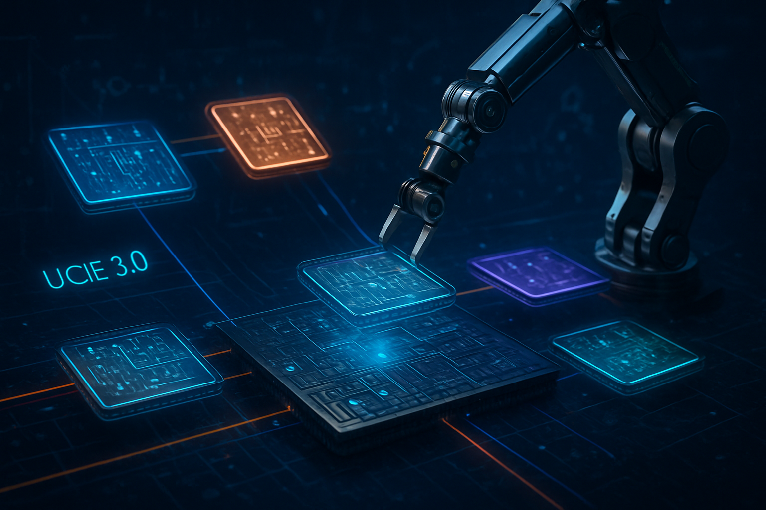
    The $200 million project involves a 110,000-square-foot expansion of the existing Spokane Valley site, specifically designed to meet the rigorous standards of sub-5nm chip fabrication. At the heart of this expansion is the production of sputtering targets—discs of ultra-pure metals and alloys used in Physical Vapor Deposition (PVD) processes. These materials are "sputtered" onto silicon wafers to form the conductive pathways that allow transistors to communicate. As AI chips become increasingly complex, requiring denser interconnects and higher thermal efficiency, the purity and consistency of these targets have become a primary bottleneck in chip yields.

    Technically, the new facility distinguishes itself through a "Digital Twin" manufacturing approach. Solstice is integrating real-time IoT monitoring and AI-driven predictive maintenance across its production lines to ensure that every target meets atomic-level specifications. Furthermore, the expansion introduces 100% laser-vision quality inspection systems, which replace traditional sampling methods. This shift allows for unprecedented traceability, ensuring that a chipmaker in Arizona or Ohio can trace the specific metallurgical profile of the material used in their most sensitive logic gates back to the Spokane floor.

    Initial reactions from the semiconductor research community have been overwhelmingly positive. Materials scientists note that Solstice’s focus on "circular production"—a system designed to reclaim and refine precious metals from spent targets—is a technical breakthrough in sustainability. By recycling used materials directly into the production loop, Solstice aims to reduce the carbon footprint of its Spokane operations by over 300 metric tons of CO2 annually, a move that aligns with the "Green Silicon" initiatives currently trending among major tech firms.

    Shifting the Competitive Landscape of Silicon

    The strategic implications of this expansion ripple across the entire tech sector. For major chip fabricators like Intel Corporation (NASDAQ: INTC) and Taiwan Semiconductor Manufacturing Company (NYSE: TSM), a robust domestic supply of sputtering targets reduces lead times and mitigates the risks associated with trans-Pacific logistics. In an era where geopolitical tensions can disrupt supply chains overnight, having a "Tier 1" materials supplier within the Pacific Northwest’s "Silicon Forest" provides a significant competitive advantage for U.S.-based manufacturing hubs.

    Solstice’s move also puts pressure on international competitors, particularly those based in Asia and Europe. By modernizing its Spokane facility with advanced automation, Solstice is effectively lowering the cost-per-unit while increasing quality, challenging the traditional dominance of overseas suppliers who have historically relied on lower labor costs. For AI startups and specialized chip designers, this expansion means more predictable access to the high-end materials needed for custom AI accelerators, potentially lowering the barrier to entry for hardware innovation.

    Furthermore, the spinoff of Solstice from Honeywell has allowed the entity to operate with the agility of a pure-play materials company. This focus is already paying dividends; the company has reportedly secured long-term supply agreements with several "Magnificent Seven" tech companies that are increasingly designing their own in-house AI silicon. By positioning itself as a neutral, high-capacity provider, Solstice is becoming the "arms dealer" for the AI hardware wars.

    A Blueprint for Regional Tech Ecosystems

    The Spokane expansion is a microcosm of the national effort to rebuild the American industrial base through the lens of high technology. Following the momentum of the CHIPS and Science Act, this project demonstrates how mid-sized cities can become integral nodes in the global AI economy. Spokane’s transformation from a traditional manufacturing town to a high-tech materials hub provides a blueprint for other regions looking to capitalize on the onshoring trend. The injection of $80 million into local Washington-based suppliers alone is expected to create a "multiplier effect," fostering a cluster of specialized logistics, maintenance, and engineering firms around the Solstice campus.

    However, the rapid growth of such facilities also brings potential concerns, primarily regarding the "war for talent." With the expansion expected to create over 80 high-tech roles and hundreds of support positions, the local educational infrastructure—including Washington State University and Eastern Washington University—is under pressure to accelerate its semiconductor engineering programs. There are also broader concerns about the environmental impact of chemical processing, though Solstice’s commitment to circular manufacturing and water reclamation has so far mitigated local opposition.

    Comparatively, this expansion mirrors the "Gigafactory" model seen in the electric vehicle industry, where vertical integration and local supply chains are prioritized to ensure stability. Just as battery materials were the focus of the 2010s, semiconductor materials are becoming the strategic frontier of the 2020s. The Spokane facility is a clear signal that the U.S. is no longer content to simply design chips; it intends to master the physical substances that make them possible.

    The Road to 2029 and Beyond

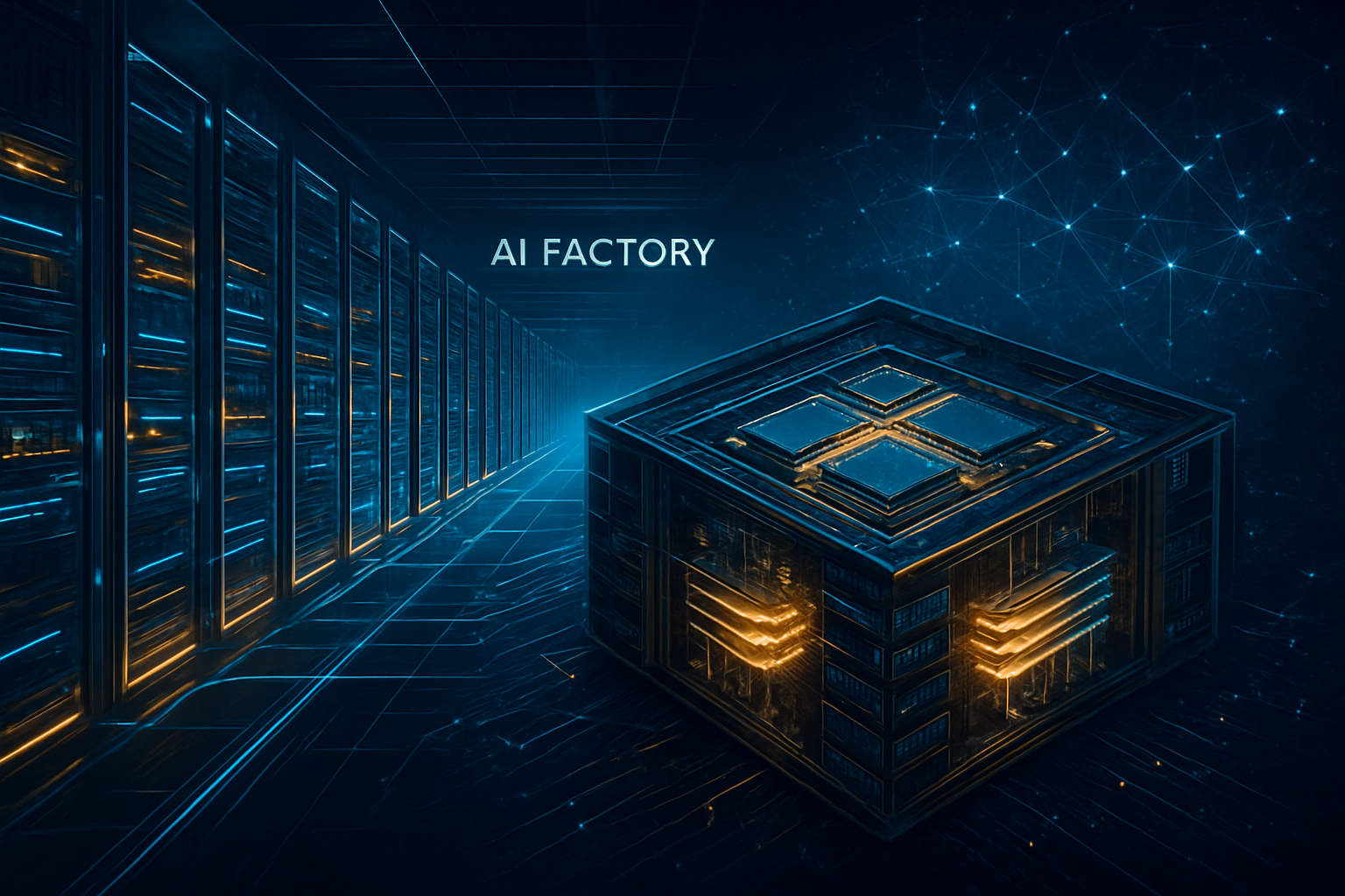
    Looking ahead, the Spokane facility is scheduled to reach full operational capacity by 2029. In the near term, the industry can expect a series of incremental rollouts as new automated lines come online. One of the most anticipated developments is the production of specialized targets for "3D-stacked" memory and logic, a technology essential for the massive bandwidth requirements of Large Language Models (LLMs). As AI models grow in size, the hardware must evolve to include more vertical layers, and Solstice’s new facility is specifically geared toward the materials required for these complex architectures.

    Experts predict that Solstice’s success in Spokane will trigger a wave of similar investments across the Inland Northwest. We may soon see a "clustering effect" where chemical suppliers and wafer testing facilities co-locate near Solstice to further minimize transit times. The ultimate challenge will be maintaining this momentum as global economic conditions fluctuate. However, given the seemingly insatiable demand for AI compute, the long-term outlook for the Spokane site remains exceptionally strong.

    A New Chapter for the Silicon Forest

    The $200 million expansion by Solstice Advanced Materials represents a definitive stake in the ground for American semiconductor independence. By bridging the gap between raw metallurgy and advanced AI logic, the Spokane facility is securing its place in the history of the current technological epoch. It is a reminder that while the "cloud" may feel ethereal, it is built on a foundation of precisely engineered physical matter.

    As we move into 2026, the industry will be watching Solstice closely to see if it can meet its ambitious production timelines and if its circular manufacturing model can truly set a new standard for the industry. For Spokane, the message is clear: the city is no longer on the periphery of the tech world; it is at the very center of the hardware that will define the next decade of human innovation.


    This content is intended for informational purposes only and represents analysis of current AI developments.

    TokenRing AI delivers enterprise-grade solutions for multi-agent AI workflow orchestration, AI-powered development tools, and seamless remote collaboration platforms.
    For more information, visit https://www.tokenring.ai/.

  • The Silicon Foundation: How Advanced Wafer Technology and Strategic Sourcing are Powering the 2026 AI Surge

    The Silicon Foundation: How Advanced Wafer Technology and Strategic Sourcing are Powering the 2026 AI Surge

    As the artificial intelligence industry moves into its "Industrialization Phase" in late 2025, the focus has shifted from high-level model architectures to the fundamental physical constraints of computing. The announcement of a comprehensive new resource from Stanford Advanced Materials (SAM), titled "Silicon Wafer Technology and Supplier Selection," marks a pivotal moment for hardware engineers and procurement teams. This guide arrives at a critical juncture where the success of next-generation AI accelerators, such as the upcoming Rubin architecture from NVIDIA (NASDAQ: NVDA), depends entirely on the microscopic perfection of the silicon substrates beneath them.

    The immediate significance of this development lies in the industry's transition to 2nm and 1.4nm process nodes. At these infinitesimal scales, the silicon wafer is no longer a passive carrier but a complex, engineered component that dictates power efficiency, thermal management, and—most importantly—manufacturing yield. As AI labs demand millions of high-performance chips, the ability to source ultra-pure, perfectly flat wafers has become the ultimate competitive moat, separating the leaders of the silicon age from those struggling with supply chain bottlenecks.

    The Technical Frontier: 11N Purity and Backside Power Delivery

    The technical specifications for silicon wafers in late 2025 have reached levels of precision previously thought impossible. According to the new SAM resources, the industry benchmark for advanced logic nodes has officially moved to 11N purity (99.999999999%). This level of decontamination is essential for the Gate-All-Around (GAA) transistor architectures used by Taiwan Semiconductor Manufacturing Company (NYSE: TSM) and Samsung Electronics (KRX: 005930). At this scale, even a single foreign atom can cause a catastrophic failure in the ultra-fine circuitry of an AI processor.

    Beyond purity, the SAM guide highlights the rise of specialized substrates like Epitaxial (Epi) wafers and Fully Depleted Silicon-on-Insulator (FD-SOI). Epi wafers are now critical for the implementation of Backside Power Delivery (BSPDN), a breakthrough technology that moves power routing to the rear of the wafer to reduce "routing congestion" on the front. This allows for more dense transistor placement, directly enabling the massive parameter counts of 2026-class Large Language Models (LLMs). Furthermore, the guide details the requirement for "ultra-flatness," where the Total Thickness Variation (TTV) must be less than 0.3 microns to accommodate the extremely shallow depth of focus in High-NA EUV lithography machines.

    Strategic Shifts: From Transactions to Foundational Partnerships

    This advancement in wafer technology is forcing a radical shift in how tech giants and startups approach their supply chains. Major players like Intel (NASDAQ: INTC) and NVIDIA are moving away from transactional purchasing toward what SAM calls "Foundational Technology Partnerships." In this model, chip designers and wafer suppliers collaborate years in advance to tailor substrate characteristics—such as resistivity and crystal orientation—to the specific needs of a chip's architecture.

    The competitive implications are profound. Companies that secure "priority capacity" for 300mm wafers with advanced Epi layers will have a significant advantage in bringing their chips to market. We are also seeing a "Shift Left" strategy, where procurement teams are prioritizing regional hubs to mitigate geopolitical risks. For instance, the expansion of GlobalWafers (TWO: 6488) in the United States, supported by the CHIPS Act, has become a strategic anchor for domestic fabrication sites in Arizona and Texas. Startups that fail to adopt these sophisticated supplier selection strategies risk being "priced out" or "waited out" as the 9.2 million wafer-per-month global capacity is increasingly pre-allocated to the industry's titans.

    Geopolitics and the Sustainability of the AI Boom

    The wider significance of these wafer advancements extends into the realms of geopolitics and environmental sustainability. The silicon wafer is the first link in the AI value chain, and its production is concentrated in a handful of high-tech facilities. The SAM guide emphasizes that "Geopolitical Resilience" is now a top-tier metric in supplier selection, reflecting the ongoing tensions over semiconductor sovereignty. As nations race to build "sovereign AI" clouds, the demand for locally sourced, high-grade silicon has turned a commodity market into a strategic battlefield.

    Furthermore, the environmental impact of wafer production is under intense scrutiny. The Czochralski (CZ) process used to grow silicon crystals is energy-intensive and requires vast amounts of ultrapure water. In response, the latest industry standards highlighted by SAM prioritize suppliers that utilize AI-driven manufacturing to reduce chemical waste and implement closed-loop water recycling. This shift ensures that the AI revolution does not come at an unsustainable environmental cost, aligning the hardware industry with global ESG (Environmental, Social, and Governance) mandates that have become mandatory for public investment in 2025.

    The Horizon: 450mm Wafers and 2D Materials

    Looking ahead, the industry is already preparing for the next set of challenges. While 300mm wafers remain the standard, research into Panel-Level Packaging—utilizing 600mm x 600mm square substrates—is gaining momentum as a way to increase the yield of massive AI die sizes. Experts predict that the next three years will see the integration of 2D materials like molybdenum disulfide (MoS2) directly onto silicon wafers, potentially allowing for "3D stacked" logic that could bypass the physical limits of current transistor scaling.

    However, these future applications face significant hurdles. The transition to larger formats or exotic materials requires a multi-billion dollar overhaul of the entire lithography and etching ecosystem. The consensus among industry analysts is that the near-term focus will remain on refining the "Advanced Packaging" interface, where the quality of the silicon interposer—the bridge between the chip and its memory—is just as critical as the processor wafer itself.

    Conclusion: The Bedrock of the Intelligence Age

    The release of the Stanford Advanced Materials resources serves as a stark reminder that the "magic" of artificial intelligence is built on a foundation of material science. As we have seen, the difference between a world-leading AI model and a failed product often comes down to the sub-micron flatness and 11N purity of a silicon disk. The advancements in wafer technology and the evolution of supplier selection strategies are not merely technical footnotes; they are the primary drivers of the AI economy.

    In the coming months, keep a close watch on the quarterly earnings of major wafer suppliers and the progress of "backside power" integration in consumer and data center chips. As the industry prepares for the 1.4nm era, the companies that master the complexities of the silicon substrate will be the ones that define the next decade of human innovation.


    This content is intended for informational purposes only and represents analysis of current AI developments.

    TokenRing AI delivers enterprise-grade solutions for multi-agent AI workflow orchestration, AI-powered development tools, and seamless remote collaboration platforms.
    For more information, visit https://www.tokenring.ai/.

  • Dismantling the Memory Wall: How HBM4 and Processing-in-Memory Are Re-Architecting the AI Era

    Dismantling the Memory Wall: How HBM4 and Processing-in-Memory Are Re-Architecting the AI Era

    As the artificial intelligence industry closes out 2025, the narrative of "bigger is better" regarding compute power has shifted toward a more fundamental physical constraint: the "Memory Wall." For years, the raw processing speed of GPUs has outpaced the rate at which data can be moved from memory to the processor, leaving the world’s most advanced AI chips idling for significant portions of their operation. However, a series of breakthroughs in late 2025—headlined by the mass production of HBM4 and the commercial debut of Processing-in-Memory (PIM) architectures—marks a pivotal moment where the industry is finally beginning to dismantle this bottleneck.

    The immediate significance of these developments cannot be overstated. As Large Language Models (LLMs) like GPT-5 and Llama 4 push toward multi-trillion parameter scales, the cost and energy required to move data between components have become the primary limiters of AI performance. By integrating compute capabilities directly into the memory stack and doubling the data bus width, the industry is moving from a "compute-centric" to a "memory-centric" architecture. This shift is expected to reduce the energy consumption of AI inference by up to 70%, effectively extending the life of current data center power grids while enabling the next generation of "Agentic AI" that requires massive, persistent memory contexts.

    The Technical Breakthrough: HBM4 and the 2,048-Bit Leap

    The technical cornerstone of this evolution is High Bandwidth Memory 4 (HBM4). Unlike its predecessor, HBM3E, which utilized a 1,024-bit interface, HBM4 doubles the width of the data highway to 2,048 bits. This change, showcased prominently at the Supercomputing Conference (SC25) in November, allows for bandwidths exceeding 2 TB/s per stack. SK Hynix (KRX: 000660) led the charge this year by demonstrating the world's first 12-layer HBM4 stacks, which utilize a base logic die manufactured on advanced foundry processes to manage the massive data flow.

    Beyond raw bandwidth, the emergence of Processing-in-Memory (PIM) represents a radical departure from the traditional Von Neumann architecture, where the CPU/GPU and memory are separate entities. Technologies like SK Hynix's AiMX and Samsung (KRX: 005930) Mach-1 are now embedding AI processing units directly into the memory chips themselves. This allows the memory to handle specific tasks—such as the "Attention" mechanisms in LLMs or Key-Value (KV) cache management—without ever sending the data back to the main GPU. By performing these operations "in-place," PIM chips eliminate the latency and energy overhead of the data bus, which has historically been the "wall" preventing real-time performance in long-context AI applications.

    Initial reactions from the research community have been overwhelmingly positive. Dr. Elena Rossi, a senior hardware analyst, noted at SC25 that "we are finally seeing the end of the 'dark silicon' era where GPUs sat waiting for data. The integration of a 4nm logic die at the base of the HBM4 stack allows for a level of customization we’ve never seen, essentially turning the memory into a co-processor." This "Custom HBM" trend allows companies like NVIDIA (NASDAQ: NVDA) to co-design the memory logic with foundries like TSMC (NYSE: TSM), ensuring that the memory architecture is perfectly tuned for the specific mathematical kernels used in modern transformer models.

    The Competitive Landscape: NVIDIA’s Rubin and the Memory Giants

    The shift toward memory-centric computing is redrawing the competitive map for tech giants. NVIDIA (NASDAQ: NVDA) remains the dominant force, but its strategy has pivoted toward a yearly release cadence to keep pace with memory advancements. The recently detailed "Rubin" R100 GPU architecture, slated for full mass production in early 2026, is designed from the ground up to leverage HBM4. With eight HBM4 stacks providing a staggering 13 TB/s of system bandwidth, NVIDIA is positioning itself not just as a chip maker, but as a system architect that controls the entire data path via its NVLink 7 interconnects.

    Meanwhile, the "Memory War" between SK Hynix, Samsung, and Micron (NASDAQ: MU) has reached a fever pitch. Samsung, which trailed in the HBM3E cycle, has signaled a massive comeback in December 2025 by reporting 90% yields on its HBM4 logic dies. Samsung is also pushing the "AI at the edge" frontier with its SOCAMM2 and LPDDR6-PIM standards, reportedly in collaboration with Apple (NASDAQ: AAPL) to bring high-performance AI memory to future mobile devices. Micron, while slightly behind in the HBM4 ramp, announced that its 2026 supply is already sold out, underscoring the insatiable demand for high-speed memory across the industry.

    This development is also a boon for specialized AI startups and cloud providers. The introduction of CXL 3.2 (Compute Express Link) allows for "Memory Pooling," where multiple GPUs can share a massive bank of external memory. This effectively disrupts the current limitation where an AI model's size is capped by the VRAM of a single GPU. Startups focusing on inference-dedicated ASICs are now using PIM to offer "LLM-in-a-box" solutions that provide the performance of a multi-million dollar cluster at a fraction of the power and cost, challenging the dominance of traditional hyperscale data centers.

    Wider Significance: Sustainability and the Rise of Agentic AI

    The broader implications of dismantling the Memory Wall extend far beyond technical benchmarks. Perhaps the most critical impact is on sustainability. In 2024, the energy consumption of AI data centers was a growing global concern. By late 2025, the 10x to 20x reduction in "Energy per Token" enabled by PIM and HBM4 has provided a much-needed reprieve. This efficiency gain allows for the "democratization" of AI, as smaller, more efficient hardware can now run models that previously required massive power-hungry clusters.

    Furthermore, solving the memory bottleneck is the primary enabler of "Agentic AI"—systems capable of long-term reasoning and multi-step task execution. Agents require a "working memory" (the KV-cache) that can span millions of tokens. Previously, the Memory Wall made maintaining such a large context window prohibitively slow and expensive. With HBM4 and CXL-based memory pooling, AI agents can now "remember" hours of conversation or thousands of pages of documentation in real-time, moving AI from a simple chatbot interface to a truly autonomous digital colleague.

    However, this breakthrough also brings concerns. The concentration of the HBM4 supply chain in the hands of three major players (SK Hynix, Samsung, and Micron) and one major foundry (TSMC) creates a significant geopolitical and economic choke point. Furthermore, as hardware becomes more efficient, the "Jevons Paradox" may take hold: the increased efficiency could lead to even greater total energy consumption as the sheer volume of AI deployment explodes across every sector of the economy.

    The Road Ahead: 3D Stacking and Optical Interconnects

    Looking toward 2026 and beyond, the industry is already eyeing the next set of hurdles. While HBM4 and PIM have provided a temporary bridge over the Memory Wall, the long-term solution likely involves true 3D integration. Experts predict that the next major milestone will be "bumpless" bonding, where memory and logic are stacked directly on top of each other with such high density that the distinction between the two virtually disappears.

    We are also seeing the early stages of optical interconnects moving from the rack-to-rack level down to the chip-to-chip level. Companies are experimenting with using light instead of electricity to move data between the memory and the processor, which could theoretically provide infinite bandwidth with zero heat generation. In the near term, expect to see the "Custom HBM" trend accelerate, with AI labs like OpenAI and Meta (NASDAQ: META) designing their own proprietary memory logic to gain a competitive edge in model performance.

    Challenges remain, particularly in the software layer. Current programming models like CUDA are optimized for moving data to the compute; re-writing these frameworks to support "computing in the memory" is a monumental task that the industry is only beginning to address. Nevertheless, the consensus among experts is clear: the architecture of the next decade of AI will be defined not by how fast we can calculate, but by how intelligently we can store and move data.

    A New Foundation for Intelligence

    The dismantling of the Memory Wall marks a transition from the "Brute Force" era of AI to the "Architectural Refinement" era. By doubling bandwidth with HBM4 and bringing compute to the data through PIM, the industry has successfully bypassed a physical limit that many feared would stall AI progress by 2025. This achievement is as significant as the transition from CPUs to GPUs was a decade ago, providing the physical foundation necessary for the next leap in machine intelligence.

    As we move into 2026, the success of these technologies will be measured by their deployment in the wild. Watch for the first HBM4-powered "Rubin" systems to hit the market and for the integration of PIM into consumer devices, which will signal the arrival of truly capable on-device AI. The Memory Wall has not been completely demolished, but for the first time in the history of modern computing, we have found a way to build a door through it.


    This content is intended for informational purposes only and represents analysis of current AI developments.

    TokenRing AI delivers enterprise-grade solutions for multi-agent AI workflow orchestration, AI-powered development tools, and seamless remote collaboration platforms.
    For more information, visit https://www.tokenring.ai/.

  • The Great Silicon Migration: Global Semiconductor Maps Redrawn as US and India Hit Key Milestones

    The Great Silicon Migration: Global Semiconductor Maps Redrawn as US and India Hit Key Milestones

    The global semiconductor landscape has reached a historic turning point. As of late 2025, the multi-year effort to diversify the world’s chip supply chain away from its heavy concentration in Taiwan has transitioned from a series of legislative promises into a tangible, operational reality. With the United States successfully bringing its first advanced "onshored" logic fabs online and India emerging as a critical hub for back-end assembly, the geographical monopoly on high-end silicon is finally beginning to fracture. This shift represents the most significant restructuring of the technology industry’s physical foundation in over four decades, driven by a combination of geopolitical de-risking and the insatiable hardware demands of the generative AI era.

    The immediate significance of this migration cannot be overstated for the AI industry. For years, the concentration of advanced node production in a single geographic region—Taiwan—posed a systemic risk to global stability and the AI revolution. Today, the successful volume production of 4nm chips at Taiwan Semiconductor Manufacturing Co. (NYSE: TSM)'s Arizona facility and the commencement of 1.8nm-class production by Intel Corporation (NASDAQ: INTC) mark the birth of a "Silicon Heartland" in the West. These developments provide a vital safety valve for AI giants like NVIDIA (NASDAQ: NVDA) and Advanced Micro Devices (NASDAQ: AMD), ensuring that the next generation of AI accelerators will have a diversified manufacturing base.

    Advanced Logic Moves West: The Technical Frontier

    The technical achievements of 2025 have silenced many skeptics who doubted the feasibility of migrating ultra-advanced manufacturing processes to U.S. soil. TSMC’s Fab 21 in Arizona is now in full volume production of 4nm (N4P) chips, achieving yields that are reportedly identical to those in its Hsinchu headquarters. This facility is currently supplying the high-performance silicon required for the latest mobile processors and AI edge devices. Meanwhile, Intel has reached a critical milestone with its 18A (1.8nm) node in Oregon and Arizona. By utilizing revolutionary RibbonFET gate-all-around (GAA) transistors and PowerVia backside power delivery, Intel has managed to leapfrog traditional scaling limits, positioning its foundry services as a direct competitor to TSMC for the most demanding AI workloads.

    In contrast to the U.S. focus on leading-edge logic, the diversification effort in Europe and India has taken a more specialized technical path. In Europe, the European Chips Act has fostered a stronghold in "foundational" nodes. The ESMC project in Dresden—a joint venture between TSMC, Infineon Technologies (OTCMKTS: IFNNY), NXP Semiconductors (NASDAQ: NXPI), and Robert Bosch GmbH—is currently installing equipment for 28nm and 16nm FinFET production. These nodes are technically optimized for the high-reliability requirements of the automotive and industrial sectors, ensuring that the European AI-driven automotive industry is not paralyzed by future supply shocks.

    India has carved out a unique position by focusing on the "back-end" of the supply chain and foundational logic. The Tata Group's first commercial-scale fab in Dholera, Gujarat, is currently under construction with a focus on 28nm nodes, which are essential for power management and communication chips. More importantly, Micron Technology (NASDAQ: MU) has successfully operationalized its $2.7 billion assembly, testing, marking, and packaging (ATMP) facility in Sanand, Gujarat. This facility is the first of its kind in India, handling the complex final stages of memory production that are critical for High Bandwidth Memory (HBM) used in AI data centers.

    Strategic Advantages for the AI Ecosystem

    This geographic redistribution of manufacturing capacity creates a new competitive dynamic for AI companies and tech giants. For companies like Apple (NASDAQ: AAPL) and Nvidia, the ability to source chips from multiple jurisdictions provides a powerful strategic hedge. It reduces the "single-source" risk that has long been a vulnerability in their SEC filings. By having access to TSMC’s Arizona fabs and Intel’s 18A capacity, these companies can better negotiate pricing and ensure a steady supply of silicon even in the event of regional instability in East Asia.

    The competitive implications are particularly stark for the foundry market. Intel’s successful rollout of its 18A node has transformed it into a credible "Western Foundry" alternative, attracting interest from AI startups and established labs that prioritize domestic security and IP protection. Conversely, Samsung Electronics (OTCMKTS: SSNLF) has made a strategic pivot at its Taylor, Texas facility, delaying 4nm production to move directly to 2nm (SF2) nodes by 2026. This "leapfrog" strategy is designed to capture the next wave of AI accelerator contracts, as the industry moves beyond current-generation architectures toward more energy-efficient 2nm designs.

    Geopolitics and the New Silicon Map

    The wider significance of these developments lies in the decoupling of the technology supply chain from geopolitical flashpoints. For decades, the "Silicon Shield" of Taiwan was seen as a deterrent to conflict, but the AI boom has made chip supply a matter of national security. The diversification into the U.S., Europe, and India represents a shift toward "friend-shoring," where manufacturing is concentrated in allied nations. This trend, however, has not been without its setbacks. The mid-2025 cancellation of Intel’s planned mega-fabs in Germany and Poland served as a sobering reminder that economic reality and corporate restructuring can still derail even the most ambitious government-backed plans.

    Despite these hurdles, the broader trend is clear: the era of extreme concentration is ending. This fits into a larger pattern of "resilience over efficiency" that has characterized the post-pandemic global economy. While building chips in Arizona or Dresden is undeniably more expensive than in Taiwan or South Korea, the industry has collectively decided that the cost of a total supply chain collapse is infinitely higher. This mirrors previous shifts in other critical industries, such as energy and aerospace, where geographic redundancy is considered a baseline requirement for survival.

    The Road Ahead: 1.4nm and Beyond

    Looking toward 2026 and 2027, the focus will shift from building "shells" to installing the next generation of lithography equipment. The deployment of ASML (NASDAQ: ASML)'s High-NA EUV (Extreme Ultraviolet) scanners will be the next major battleground. Intel’s Ohio "Silicon Heartland" site, though facing structural delays, is being prepared as a primary hub for 14A (1.4nm) production using these advanced tools. Experts predict that the next three years will see a "capacity war" as regions compete to prove they can not only build the chips but also sustain the complex ecosystem of chemicals, gases, and specialized labor required to keep the fabs running.

    One of the most significant challenges remaining is the talent gap. Both the U.S. and India are racing to train tens of thousands of specialized engineers required to operate these facilities. The success of the India Semiconductor Mission (ISM) will depend heavily on its ability to transition from assembly and testing into high-end wafer fabrication. If India can successfully bring the Tata-PSMC fab online by 2027, it will cement its place as the third major pillar of the global semiconductor supply chain, alongside East Asia and the West.

    A New Era of Hardware Sovereignty

    The events of 2025 mark the end of the first chapter of the "Great Silicon Migration." The key takeaway is that the global semiconductor map has been successfully redrawn. While Taiwan remains the undisputed leader in volume and advanced node expertise, it is no longer the world’s only option. The operational status of TSMC Arizona and the emergence of India’s assembly ecosystem have created a more resilient, albeit more expensive, foundation for the future of artificial intelligence.

    In the coming months, industry watchers should keep a close eye on the yield rates of Samsung’s 2nm pivot in Texas and the progress of the ESMC project in Germany. These will be the litmus tests for whether the diversification effort can maintain its momentum without the massive government subsidies that characterized its early years. For now, the AI industry can breathe a sigh of relief: the physical infrastructure of the digital age is finally starting to look as global as the code that runs upon it.


    This content is intended for informational purposes only and represents analysis of current AI developments.

    TokenRing AI delivers enterprise-grade solutions for multi-agent AI workflow orchestration, AI-powered development tools, and seamless remote collaboration platforms.
    For more information, visit https://www.tokenring.ai/.

  • The Memory Wall: Why HBM4 is the New Frontier in the Global AI Arms Race

    The Memory Wall: Why HBM4 is the New Frontier in the Global AI Arms Race

    As of late 2025, the artificial intelligence revolution has reached a critical inflection point where the speed of silicon is no longer the primary constraint. Instead, the industry’s gaze has shifted to the "Memory Wall"—the physical limit of how fast data can move between a processor and its memory. High Bandwidth Memory (HBM) has emerged as the most precious commodity in the tech world, serving as the essential fuel for the massive Large Language Models (LLMs) and generative AI systems that now define the global economy.

    The announcement of Nvidia’s (NASDAQ: NVDA) upcoming "Rubin" architecture, which utilizes the next-generation HBM4 standard, has sent shockwaves through the semiconductor industry. With HBM supply already sold out through most of 2026, the competition between the world’s three primary producers—SK Hynix, Micron, and Samsung—has escalated into a high-stakes battle for dominance in a market that is fundamentally reshaping the hardware landscape.

    The Technical Leap: From HBM3e to the 2048-bit HBM4 Era

    The technical specifications of HBM in late 2025 reveal a staggering jump in capability. While HBM3e was the workhorse of the Blackwell GPU generation, offering roughly 1.2 TB/s of bandwidth per stack, the new HBM4 standard represents a paradigm shift. The most significant advancement is the doubling of the memory interface width from 1024-bit to 2048-bit. This allows HBM4 to achieve bandwidths exceeding 2.0 TB/s per stack while maintaining lower clock speeds, a crucial factor in managing the extreme heat generated by 12-layer and 16-layer 3D-stacked dies.

    This generational shift is not just about speed; it is about capacity and physical integration. As of December 2025, the industry has transitioned to "1c" DRAM nodes (approximately 10nm), enabling capacities of up to 64GB per stack. Furthermore, the integration process has evolved. Using TSMC’s (NYSE: TSM) System on Integrated Chips (SoIC) and "bumpless" hybrid bonding, HBM4 stacks are now placed within microns of the GPU logic die. This proximity drastically reduces electrical impedance and power consumption, which had become a major barrier to scaling AI clusters.

    Industry experts note that this transition is technically grueling. The shift to HBM4 requires a total redesign of the base logic die—the foundation upon which memory layers are stacked. Unlike previous generations where the logic die was relatively simple, HBM4 logic dies are increasingly being manufactured on advanced 5nm or 3nm foundry processes to handle the complex routing required for the 2048-bit interface. This has turned HBM from a "commodity" component into a semi-custom processor in its own right.

    The Titan Triumvirate: SK Hynix, Micron, and Samsung’s Power Struggle

    The competitive landscape of late 2025 is dominated by an intense three-way rivalry. SK Hynix (KRX: 000660) currently holds the throne with an estimated 55–60% market share. Their early bet on Mass Reflow Molded Underfill (MR-MUF) packaging technology has paid off, providing superior thermal dissipation that has made them the preferred partner for Nvidia’s Blackwell Ultra (B300) systems. In December 2025, SK Hynix became the first to ship verified HBM4 samples for the Rubin platform, solidifying its lead.

    Micron (NASDAQ: MU) has successfully cemented itself as the primary challenger, holding approximately 20–25% of the market. Micron’s 12-layer HBM3e stacks gained widespread acclaim in early 2025 for their industry-leading power efficiency, which allowed data center operators to squeeze more performance out of existing power envelopes. However, as the industry moves toward HBM4, Micron faces the challenge of scaling its "1c" node yields to match the aggressive production schedules of major cloud providers like Microsoft (NASDAQ: MSFT) and Google (NASDAQ: GOOGL).

    Samsung (KRX: 005930), after a period of qualification delays in 2024, has mounted a massive comeback in late 2025. Samsung is playing a unique strategic card: the "One-Stop Shop." As the only company that possesses both world-class DRAM manufacturing and a leading-edge logic foundry, Samsung is offering "Custom HBM" solutions. By manufacturing both the memory layers and the specialized logic die in-house, Samsung aims to bypass the complex supply chain coordination required between memory makers and external foundries like TSMC, a move that is gaining traction with hyperscalers looking for bespoke AI silicon.

    The Critical Link: Why LLMs Live and Die by Memory Bandwidth

    The criticality of HBM for generative AI cannot be overstated. In late 2025, the AI industry has bifurcated its needs into two distinct categories: training and inference. For training trillion-parameter models, bandwidth is the absolute priority. Without the 13.5 TB/s aggregate bandwidth provided by HBM4-equipped GPUs, the thousands of processing cores inside an AI chip would spend a significant portion of their cycles "starving" for data, leading to massive inefficiencies in multi-billion dollar training runs.

    For inference, the focus has shifted toward capacity. The rise of "Agentic AI" and long-context windows—where models can remember and process up to 2 million tokens of information—requires massive amounts of VRAM to store the "KV Cache" (the model's short-term memory). A single GPU now needs upwards of 288GB of HBM to handle high-concurrency requests for complex agents. This demand has led to a persistent supply shortage, with lead times for HBM-equipped hardware exceeding 40 weeks for smaller firms.

    Furthermore, the HBM boom is having a "cannibalization" effect on the broader tech industry. Because HBM requires roughly three times the wafer area of standard DDR5 memory, the surge in AI demand has restricted the supply of PC and server RAM. As of December 2025, commodity DRAM prices have surged by over 60% year-over-year, impacting everything from consumer laptops to enterprise cloud storage. This "AI tax" is now a standard consideration for IT departments worldwide.

    Future Horizons: Custom Logic and the Road to HBM5

    Looking ahead to 2026 and beyond, the roadmap for HBM is moving toward even deeper integration. The next phase, often referred to as HBM4e, is expected to push capacities toward 80GB per stack. However, the more profound change will be the "logic-on-memory" trend. Experts predict that future HBM stacks will incorporate specialized AI accelerators directly into the base logic die, allowing for "near-memory computing" where simple data processing tasks are handled within the memory stack itself, further reducing the need to move data back and forth to the main GPU.

    Challenges remain, particularly regarding yield and cost. Producing HBM4 at the "1c" node is proving to be one of the most difficult manufacturing feats in semiconductor history. Current yields for 16-layer stacks are reportedly hovering around 60%, meaning nearly half of the highly expensive wafers are discarded. Addressing these yield issues will be the primary focus for engineers in the coming months, as any improvement directly translates to millions of dollars in additional revenue for the manufacturers.

    The Final Verdict on the HBM Revolution

    High Bandwidth Memory has transitioned from a niche hardware specification to the geopolitical and economic linchpin of the AI era. As we close out 2025, it is clear that the companies that control the memory supply—SK Hynix, Micron, and Samsung—hold as much power over the future of AI as the companies designing the chips or the models themselves. The shift to HBM4 marks a new chapter where memory is no longer just a storage medium, but a sophisticated, high-performance compute platform.

    In the coming months, the industry should watch for the first production benchmarks of Nvidia’s Rubin GPUs and the success of Samsung’s integrated foundry-memory model. As AI models continue to grow in complexity and context, the "Memory Wall" will either be the barrier that slows progress or, through the continued evolution of HBM, the foundation upon which the next generation of digital intelligence is built.


    This content is intended for informational purposes only and represents analysis of current AI developments.

    TokenRing AI delivers enterprise-grade solutions for multi-agent AI workflow orchestration, AI-powered development tools, and seamless remote collaboration platforms.
    For more information, visit https://www.tokenring.ai/.

  • The Great Unbundling of Silicon: How UCIe 3.0 is Powering a New Era of ‘Mix-and-Match’ AI Hardware

    The Great Unbundling of Silicon: How UCIe 3.0 is Powering a New Era of ‘Mix-and-Match’ AI Hardware

    The semiconductor industry has reached a pivotal turning point as the Universal Chiplet Interconnect Express (UCIe) standard enters full commercial maturity. As of late 2025, the release of the UCIe 3.0 specification has effectively dismantled the era of monolithic, "black box" processors, replacing it with a modular "mix and match" ecosystem. This development allows specialized silicon components—known as chiplets—from different manufacturers to be housed within a single package, communicating at speeds that were previously only possible within a single piece of silicon. For the artificial intelligence sector, this represents a massive leap forward, enabling the construction of hyper-specialized AI accelerators that can scale to meet the insatiable compute demands of next-generation large language models (LLMs).

    The immediate significance of this transition cannot be overstated. By standardizing how these chiplets communicate, the industry is moving away from proprietary, vendor-locked architectures toward an open marketplace. This shift is expected to slash development costs for custom AI silicon by up to 40% and reduce time-to-market by nearly a year for many fabless design firms. As the AI hardware race intensifies, UCIe 3.0 provides the "lingua franca" that ensures an I/O die from one vendor can work seamlessly with a compute engine from another, all while maintaining the ultra-low latency required for real-time AI inference and training.

    The Technical Backbone: From UCIe 1.1 to the 64 GT/s Breakthrough

    The technical evolution of the UCIe standard has been rapid, culminating in the August 2025 release of the UCIe 3.0 specification. While UCIe 1.1 focused on basic reliability and health monitoring for automotive and data center applications, and UCIe 2.0 introduced standardized manageability and 3D packaging support, the 3.0 update is a game-changer for high-performance computing. It doubles the data rate to 64 GT/s per lane, providing the massive throughput necessary for the "XPU-to-memory" bottlenecks that have plagued AI clusters. A key innovation in the 3.0 spec is "Runtime Recalibration," which allows links to dynamically adjust power and performance without requiring a system reboot—a critical feature for massive AI data centers that must remain operational 24/7.

    This new standard differs fundamentally from previous approaches like Intel Corporation (NASDAQ: INTC)’s proprietary Advanced Interface Bus (AIB) or Advanced Micro Devices, Inc. (NASDAQ: AMD)’s early Infinity Fabric. While those technologies proved the viability of chiplets, they were "closed loops" that prevented cross-vendor interoperability. UCIe 3.0, by contrast, defines everything from the physical layer (the actual wires and bumps) to the protocol layer, ensuring that a chiplet designed by a startup can be integrated into a larger system-on-chip (SoC) manufactured by a giant like NVIDIA Corporation (NASDAQ: NVDA). Initial reactions from the research community have been overwhelmingly positive, with engineers at the Open Compute Project (OCP) hailing it as the "PCIe moment" for internal chip communication.

    The Competitive Landscape: Giants and Challengers Align

    The shift toward a standardized chiplet ecosystem is creating a new hierarchy among tech giants. Intel Corporation (NASDAQ: INTC) has been the most aggressive proponent, having donated the initial specification to the consortium. Their recent launch of the Granite Rapids-D (Xeon 6 SoC) in early 2025 stands as one of the first high-volume products to fully leverage UCIe for modularity at the edge. Meanwhile, NVIDIA Corporation (NASDAQ: NVDA) has adapted its strategy; while it still champions its proprietary NVLink for high-end GPU clusters, it recently released "UCIe-ready" silicon bridges. These bridges allow customers to build custom AI accelerators that can talk directly to NVIDIA’s Blackwell and upcoming Rubin architectures, effectively turning NVIDIA’s hardware into a platform for third-party innovation.

    Taiwan Semiconductor Manufacturing Company (NYSE: TSM) and Samsung Electronics (KRX: 005930) are currently locked in a "foundry race" to provide the packaging technology that makes UCIe possible. TSMC’s 3DFabric and Samsung’s I-Cube/X-Cube technologies are the physical stages where these mix-and-match chiplets perform. In mid-2025, Samsung successfully demonstrated a 4nm chiplet prototype using IP from Synopsys, Inc. (NASDAQ: SNPS), proving that the "mix and match" dream is now a physical reality. This benefits smaller AI startups and fabless companies, who can now purchase "silicon-proven" UCIe blocks from providers like Cadence Design Systems, Inc. (NASDAQ: CDNS) instead of spending millions to design proprietary interconnect logic from scratch.

    Scaling AI: Efficiency, Cost, and the End of the "Reticle Limit"

    The broader significance of UCIe 3.0 lies in its ability to bypass the "reticle limit"—the physical size limit of a single silicon wafer die. As AI models grow, the chips needed to train them have become so large they are physically impossible to manufacture as a single piece of silicon without massive defects. By breaking the processor into smaller chiplets, manufacturers can achieve much higher yields and lower costs. This fits into the broader AI trend of "heterogeneous computing," where different parts of an AI task are handled by specialized hardware—such as a dedicated matrix multiplication die paired with a high-bandwidth memory (HBM) die and a low-power I/O die.

    However, this transition is not without concerns. The primary challenge remains "Standardized Manageability"—the difficulty of debugging a system when the components come from five different companies. If an AI server fails, determining which vendor’s chiplet caused the error becomes a complex legal and technical nightmare. Furthermore, while UCIe 3.0 provides the physical connection, the software stack required to manage these disparate components is still in its infancy. Despite these hurdles, the move toward UCIe is being compared to the transition from mainframe computers to modular PCs; it is an "unbundling" that democratizes high-performance silicon.

    The Horizon: Optical I/O and the 'Chiplet Store'

    Looking ahead, the near-term focus will be on the integration of Optical Compute Interconnects (OCI). Intel has already demonstrated a fully integrated optical I/O chiplet using UCIe that allows chiplets to communicate via fiber optics at 4TBps over distances up to 100 meters. This effectively turns an entire data center rack into a single, giant "virtual chip." In the long term, experts predict the rise of the "Chiplet Store"—a commercial marketplace where companies can buy pre-manufactured, specialized AI chiplets (like a dedicated "Transformer Engine" or a "Security Enclave") and have them assembled by a third-party packaging house.

    The challenges that remain are primarily thermal and structural. Stacking chiplets in 3D (as supported by UCIe 2.0 and 3.0) creates intense heat pockets that require advanced liquid cooling or new materials like glass substrates. Industry analysts predict that by 2027, more than 80% of all high-end AI processors will be UCIe-compliant, as the cost of maintaining proprietary interconnects becomes unsustainable even for the largest tech companies.

    A New Blueprint for the AI Age

    The maturation of the UCIe standard represents one of the most significant architectural shifts in the history of computing. By providing a standardized, high-speed interface for chiplets, the industry has unlocked a modular future that balances the need for extreme performance with the economic realities of semiconductor manufacturing. The "mix and match" ecosystem is no longer a theoretical concept; it is the foundation upon which the next decade of AI progress will be built.

    As we move into 2026, the industry will be watching for the first "multi-vendor" AI chips to hit the market—processors where the compute, memory, and I/O are sourced from entirely different companies. This development marks the end of the monolithic era and the beginning of a more collaborative, efficient, and innovative period in silicon design. For AI companies and investors alike, the message is clear: the future of hardware is no longer about who can build the biggest chip, but who can best orchestrate the most efficient ecosystem of chiplets.


    This content is intended for informational purposes only and represents analysis of current AI developments.

    TokenRing AI delivers enterprise-grade solutions for multi-agent AI workflow orchestration, AI-powered development tools, and seamless remote collaboration platforms.
    For more information, visit https://www.tokenring.ai/.

  • The Silicon Renaissance: US Mega-Fabs Enter Operational Phase as CHIPS Act Reshapes Global AI Power

    The Silicon Renaissance: US Mega-Fabs Enter Operational Phase as CHIPS Act Reshapes Global AI Power

    As of December 18, 2025, the landscape of global technology has reached a historic inflection point. What began three years ago as a legislative ambition to reshore semiconductor manufacturing has manifested into a sprawling industrial reality across the American Sun Belt and Midwest. The implementation of the CHIPS and Science Act has moved beyond the era of press releases and groundbreaking ceremonies into a high-stakes operational phase, defined by the rise of "Mega-Fabs"—massive, multi-billion dollar complexes designed to secure the hardware foundation of the artificial intelligence revolution.

    This transition marks a fundamental shift in the geopolitical order of technology. For the first time in decades, the most advanced logic chips required for generative AI and autonomous systems are being etched onto silicon in Arizona and Ohio. However, the road to "Silicon Sovereignty" has been paved with unexpected policy pivots, including a controversial move by the U.S. government to take equity stakes in domestic champions, and a fierce race between Intel, TSMC, and Samsung to dominate the 2-nanometer (2nm) frontier on American soil.

    The Technical Frontier: 2nm Targets and High-NA EUV Integration

    The technical execution of these Mega-Fabs has become a litmus test for the next generation of computing. Intel (NASDAQ: INTC) has achieved a significant milestone at its Fab 52 in Arizona, which has officially commenced limited mass production of its 18A node (approximately 1.8nm equivalent). This node utilizes RibbonFET gate-all-around (GAA) architecture and PowerVia backside power delivery—technologies that Intel claims will provide a definitive lead over competitors in power efficiency. Meanwhile, Intel’s "Silicon Heartland" project in New Albany, Ohio, has faced structural delays, pushing its full operational status to 2030. To compensate, the Ohio site is now being outfitted with "High-NA" (High Numerical Aperture) Extreme Ultraviolet (EUV) lithography machines from ASML, skipping older generations to debut with post-14A nodes.

    TSMC (NYSE: TSM) continues to set the gold standard for operational efficiency in the U.S. Their Phoenix, Arizona, Fab 1 is currently in full high-volume production of 4nm chips, with yields reportedly matching those of its Taiwanese facilities—a feat many analysts thought impossible two years ago. In response to insatiable demand from AI giants, TSMC has accelerated the timeline for its third Arizona fab. Originally slated for the end of the decade, Fab 3 is now being fast-tracked to produce 2nm (N2) and A16 nodes by late 2028. This facility will be the first in the U.S. to utilize TSMC’s sophisticated nanosheet transistor structures at scale.

    Samsung (KRX: 005930) has taken a high-risk, high-reward approach in Taylor, Texas. After facing initial delays due to a lack of "anchor customers" for 4nm production, the South Korean giant recalibrated its strategy to skip directly to 2nm production for the site's 2026 opening. By focusing on 2nm from day one, Samsung aims to undercut TSMC on wafer pricing, targeting a cost of $20,000 per wafer compared to TSMC’s projected $30,000. This aggressive technical pivot is designed to lure AI chip designers who are looking for a domestic alternative to the TSMC monopoly.

    Market Disruptions and the New "Equity for Subsidies" Model

    The business of semiconductors has been transformed by a new "America First" industrial policy. In a landmark move in August 2025, the U.S. Department of Commerce finalized a deal to take a 9.9% equity stake in Intel (NASDAQ: INTC) in exchange for $8.9 billion in combined CHIPS Act grants and "Secure Enclave" funding. This "Equity for Subsidies" model has sent ripples through Wall Street, signaling that the U.S. government is no longer just a regulator or a customer, but a shareholder in the nation's foundry future. This move has stabilized Intel’s balance sheet during its massive Ohio expansion but has raised questions about long-term government interference in corporate strategy.

    For the primary consumers of these chips—NVIDIA (NASDAQ: NVDA), Apple (NASDAQ: AAPL), and AMD (NASDAQ: AMD)—the rise of domestic Mega-Fabs offers a strategic hedge against geopolitical instability in the Taiwan Strait. However, the transition is not without cost. While domestic production reduces the risk of supply chain decapitation, the "Silicon Renaissance" is proving expensive. Analysts estimate that chips produced in U.S. Mega-Fabs carry a 20% to 30% "reshoring premium" due to higher labor and energy costs. NVIDIA and Apple have already begun signaling that these costs will likely be passed down to enterprise customers in the form of higher prices for AI accelerators and high-end consumer hardware.

    The competitive landscape is also being reshaped by the "Trump Royalty"—a policy involving government-managed cuts on high-end AI chip exports. This has forced companies like NVIDIA to navigate a complex web of "managed access" for international sales, further incentivizing the use of U.S.-based fabs to ensure compliance with tightening national security mandates. The result is a bifurcated market where "Made in USA" silicon becomes the premium standard for security-cleared and high-performance AI applications.

    Sovereignty, Bottlenecks, and the Global AI Landscape

    The broader significance of the Mega-Fab era lies in the pursuit of AI sovereignty. As AI models become the primary engine of economic growth, the physical infrastructure that powers them has become a matter of national survival. The CHIPS Act implementation has successfully broken the 100% reliance on East Asian foundries for leading-edge logic. However, a critical vulnerability remains: the "Packaging Bottleneck." Despite the progress in fabrication, the majority of U.S.-made wafers must still be shipped to Taiwan or Southeast Asia for advanced packaging (CoWoS), which is essential for binding logic and memory into a single AI super-chip.

    Furthermore, the industry has identified a secondary crisis in High-Bandwidth Memory (HBM). While Intel and TSMC are building the "brains" of AI in the U.S., the "short-term memory"—HBM—remains concentrated in the hands of SK Hynix and Samsung’s Korean plants. Micron (NASDAQ: MU) is working to bridge this gap with its Idaho and New York expansions, but industry experts warn that HBM will remain the #1 supply chain risk for AI scaling through 2026.

    Potential concerns regarding the environmental and local impact of these Mega-Fabs have also surfaced. In Arizona and Texas, the sheer scale of water and electricity required to run these facilities is straining local infrastructure. A December 2025 report indicated that nearly 35% of semiconductor executives are concerned that the current U.S. power grid cannot sustain the projected energy needs of these sites as they reach full capacity. This has sparked a secondary boom in "SMRs" (Small Modular Reactors) and dedicated green energy projects specifically designed to power the "Silicon Heartland."

    The Road to 2030: Challenges and Future Applications

    Looking ahead, the next 24 months will focus on the "Talent War" and the integration of advanced packaging on U.S. soil. The Department of Commerce estimates a gap of 20,000 specialized cleanroom engineers needed to staff the Mega-Fabs currently under construction. Educational partnerships between chipmakers and universities in Ohio, Arizona, and Texas are being fast-tracked, but the labor shortage remains the most significant threat to the 2028-2030 production targets.

    In terms of applications, the availability of domestic 2nm and 18A silicon will enable a new class of "Edge AI" devices. We expect to see the emergence of highly autonomous robotics and localized LLM (Large Language Model) hardware that does not require cloud connectivity, powered by the low-latency, high-efficiency chips coming out of the Arizona and Texas clusters. The goal is no longer just to build chips for data centers, but to embed AI into the very fabric of American industrial and consumer infrastructure.

    Experts predict that the next phase of the CHIPS Act (often referred to in policy circles as "CHIPS 2.0") will focus heavily on these "missing links"—specifically advanced packaging and HBM manufacturing. Without these components, the Mega-Fabs remain powerful engines without a transmission, capable of producing the world's best silicon but unable to finalize the product within domestic borders.

    A New Era of Industrial Power

    The implementation of the CHIPS Act and the rise of U.S. Mega-Fabs represent the most significant shift in American industrial policy since the mid-20th century. By December 2025, the vision of a domestic "Silicon Renaissance" has moved from the halls of Congress to the cleanrooms of the Southwest. Intel, TSMC, and Samsung are now locked in a generational struggle for dominance, not just over nanometers, but over the future of the AI economy.

    The key takeaways for the coming year are clear: watch the yields at TSMC’s Arizona Fab 2, monitor the progress of Intel’s High-NA EUV installation in Ohio, and observe how Samsung’s 2nm price war impacts the broader market. While the challenges of energy, talent, and packaging remain formidable, the physical foundation for a new era of AI has been laid. The "Silicon Heartland" is no longer a slogan—it is an operational reality that will define the trajectory of technology for decades to come.


    This content is intended for informational purposes only and represents analysis of current AI developments.

    TokenRing AI delivers enterprise-grade solutions for multi-agent AI workflow orchestration, AI-powered development tools, and seamless remote collaboration platforms.
    For more information, visit https://www.tokenring.ai/.

  • The Great Decoupling: How Custom Silicon is Breaking NVIDIA’s Iron Grip on the AI Cloud

    The Great Decoupling: How Custom Silicon is Breaking NVIDIA’s Iron Grip on the AI Cloud

    As we close out 2025, the landscape of artificial intelligence infrastructure has undergone a seismic shift. For years, the industry’s reliance on NVIDIA Corp. (NASDAQ: NVDA) was absolute, with the company’s H100 and Blackwell GPUs serving as the undisputed currency of the AI revolution. However, the final months of 2025 have confirmed a new reality: the era of the "General Purpose GPU" monopoly is ending. Cloud hyperscalers—Alphabet Inc. (NASDAQ: GOOGL), Amazon.com Inc. (NASDAQ: AMZN), and Microsoft Corp. (NASDAQ: MSFT)—have successfully transitioned from being NVIDIA’s biggest customers to its most formidable competitors, deploying custom-built AI Application-Specific Integrated Circuits (ASICs) at a scale previously thought impossible.

    This transition is not merely about saving costs; it is a fundamental re-engineering of the AI stack. By bypassing traditional GPUs, these tech giants are gaining unprecedented control over their supply chains, energy consumption, and software ecosystems. With the recent launch of Google’s seventh-generation TPU, "Ironwood," and Amazon’s "Trainium3," the performance gap that once protected NVIDIA has all but vanished, ushering in a "Great Decoupling" that is redefining the economics of the cloud.

    The Technical Frontier: Ironwood, Trainium3, and the Push for 3nm

    The technical specifications of 2025’s custom silicon represent a quantum leap over the experimental chips of just two years ago. Google’s Ironwood (TPU v7), unveiled in late 2025, has become the new benchmark for scaling. Built on a cutting-edge 3nm process, Ironwood delivers a staggering 4.6 PetaFLOPS of FP8 performance per chip, narrowly edging out the standard NVIDIA Blackwell B200. What sets Ironwood apart is its "optical switching" fabric, which allows Google to link 9,216 chips into a single "Superpod" with 1.77 Petabytes of shared HBM3e memory. This architecture virtually eliminates the communication bottlenecks that plague traditional Ethernet-based GPU clusters, making it the preferred choice for training the next generation of trillion-parameter models.

    Amazon’s Trainium3, launched at re:Invent in December 2025, focuses on a different technical triumph: the "Total Cost of Ownership" (TCO). While its raw compute of 2.5 PetaFLOPS trails NVIDIA’s top-tier Blackwell Ultra, the Trainium3 UltraServer packs 144 chips into a single rack, delivering 0.36 ExaFLOPS of aggregate performance at a fraction of the power draw. Amazon’s dual-chiplet design allows for high yields and lower manufacturing costs, enabling AWS to offer AI training credits at prices 40% to 65% lower than equivalent NVIDIA-based instances.

    Microsoft, while facing some design hurdles with its Maia 200 (now expected in early 2026), has pivoted its technical strategy toward vertical integration. At Ignite 2025, Microsoft showcased the Azure Cobalt 200, a 3nm Arm-based CPU designed to work in tandem with the Azure Boost DPU (Data Processing Unit). This combination offloads networking and storage tasks from the AI accelerators, ensuring that even the current Maia 100 chips operate at near-peak theoretical utilization. This "system-level" approach differs from NVIDIA’s "chip-first" philosophy, focusing on how data moves through the entire data center rather than just the speed of a single processor.

    Market Disruption: The End of the "GPU Tax"

    The strategic implications of this shift are profound. For years, cloud providers were forced to pay what many called the "NVIDIA Tax"—massive premiums that resulted in 80% gross margins for the chipmaker. By 2025, the hyperscalers have reclaimed this margin. For Meta Platforms Inc. (NASDAQ: META), which recently began renting Google’s TPUs to supplement its own internal MTIA (Meta Training and Inference Accelerator) efforts, the move to custom silicon represents a multi-billion dollar saving in capital expenditure.

    This development has created a new competitive dynamic between major AI labs. Anthropic, backed heavily by Amazon and Google, now does the vast majority of its training on Trainium and TPU clusters. This gives them a significant cost advantage over OpenAI, which remains more closely tied to NVIDIA hardware via its partnership with Microsoft. However, even that is changing; Microsoft’s move to make its Azure Foundry "hardware agnostic" allows it to shift internal workloads like Microsoft 365 Copilot onto Maia silicon, freeing up its limited NVIDIA supply for high-paying external customers.

    Furthermore, the rise of custom ASICs is disrupting the startup ecosystem. New AI companies are no longer defaulting to CUDA (NVIDIA’s proprietary software platform). With the emergence of OpenXLA and PyTorch 2.5+, which provide seamless abstraction layers across different hardware types, the "software moat" that once protected NVIDIA is being drained. Amazon’s shocking announcement that its upcoming Trainium4 will natively support CUDA-compiled kernels is perhaps the final nail in the coffin for hardware lock-in, signaling a future where code can run on any silicon, anywhere.

    The Wider Significance: Power, Sovereignty, and Sustainability

    Beyond the corporate balance sheets, the rise of custom AI silicon addresses the most pressing crisis facing the tech industry: the power grid. As of late 2025, data centers are consuming an estimated 8% of total US electricity. Custom ASICs like Google’s Ironwood are designed with "inference-first" architectures that are up to 3x more energy-efficient than general-purpose GPUs. This efficiency is no longer a luxury; it is a requirement for obtaining building permits for new data centers in power-constrained regions like Northern Virginia and Dublin.

    This trend also reflects a broader move toward "Technological Sovereignty." During the supply chain crunches of 2023 and 2024, hyperscalers were "price takers," at the mercy of NVIDIA’s allocation schedules. In 2025, they are "price makers." By controlling the silicon design, Google, Amazon, and Microsoft can dictate their own roadmap, optimizing hardware for specific model architectures like Mixture-of-Experts (MoE) or State Space Models (SSM) that were not yet mainstream when NVIDIA’s Blackwell was first designed.

    However, this shift is not without concerns. The fragmentation of the hardware landscape could lead to a "two-tier" AI world: one where the "Big Three" cloud providers have access to hyper-efficient, low-cost custom silicon, while smaller cloud providers and sovereign nations are left competing for increasingly expensive, general-purpose GPUs. This could further centralize the power of AI development into the hands of a few trillion-dollar entities, raising antitrust questions that regulators in the US and EU are already beginning to probe as we head into 2026.

    The Horizon: Inference-First and the 2nm Race

    Looking ahead to 2026 and 2027, the focus of custom silicon is expected to shift from "Training" to "Massive-Scale Inference." As AI models become embedded in every aspect of computing—from operating systems to real-time video translation—the demand for chips that can run models cheaply and instantly will skyrocket. We expect to see "Edge-ASICs" from these hyperscalers that bridge the gap between the cloud and local devices, potentially challenging the dominance of Apple Inc. (NASDAQ: AAPL) in the AI-on-device space.

    The next major milestone will be the transition to 2nm process technology. Reports suggest that both Google and Amazon have already secured 2nm capacity at Taiwan Semiconductor Manufacturing Co. (NYSE: TSM) for 2026. These next-gen chips will likely integrate "Liquid-on-Chip" cooling technologies to manage the extreme heat densities of trillion-parameter processing. The challenge will remain software; while abstraction layers have improved, the "last mile" of optimization for custom silicon still requires specialized engineering talent that remains in short supply.

    A New Era of AI Infrastructure

    The rise of custom AI silicon marks the end of the "GPU Gold Rush" and the beginning of the "ASIC Integration" era. By late 2025, the hyperscalers have proven that they can not only match NVIDIA’s performance but exceed it in the areas that matter most: scale, cost, and efficiency. This development is perhaps the most significant in the history of AI hardware, as it breaks the bottleneck that threatened to stall AI progress due to high costs and limited supply.

    As we move into 2026, the industry will be watching closely to see how NVIDIA responds to this loss of market share. While NVIDIA remains the leader in raw innovation and software ecosystem depth, the "Great Decoupling" is now an irreversible reality. For enterprises and developers, this means more choice, lower costs, and a more resilient AI infrastructure. The AI revolution is no longer being fought on a single front; it is being won in the custom-built silicon foundries of the world’s largest cloud providers.


    This content is intended for informational purposes only and represents analysis of current AI developments.

    TokenRing AI delivers enterprise-grade solutions for multi-agent AI workflow orchestration, AI-powered development tools, and seamless remote collaboration platforms.
    For more information, visit https://www.tokenring.ai/.

  • Silicon Sovereignty: China’s Strategic Pivot to RISC-V Accelerates Amid US Tech Blockades

    Silicon Sovereignty: China’s Strategic Pivot to RISC-V Accelerates Amid US Tech Blockades

    As of late 2025, the global semiconductor landscape has reached a definitive tipping point. Driven by increasingly stringent US export controls that have severed access to high-end proprietary architectures, China has executed a massive, state-backed migration to RISC-V. This open-standard instruction set architecture (ISA) has transformed from a niche academic project into the backbone of China’s "Silicon Sovereignty" strategy, providing a critical loophole in the Western containment of Chinese AI and high-performance computing.

    The immediate significance of this shift cannot be overstated. By leveraging RISC-V, Chinese tech giants are no longer beholden to the licensing whims of Western firms or the jurisdictional reach of US export laws. This pivot has not only insulated the Chinese domestic market from further sanctions but has also sparked a rapid evolution in AI hardware design, where hardware-software co-optimization is now being used to bridge the performance gap left by the absence of top-tier Western GPUs.

    Technical Milestones and the Rise of High-Performance RISC-V

    The technical maturation of RISC-V in 2025 is headlined by Alibaba (NYSE: BABA) and its chip-design subsidiary, T-Head. In March 2025, the company unveiled the XuanTie C930, a server-grade 64-bit multi-core processor that represents a quantum leap for the architecture. Unlike its predecessors, the C930 is fully compatible with the RVA23 profile and features dual 512-bit vector units and an integrated 8 TOPS Matrix engine specifically designed for AI workloads. This allows the chip to compete directly with mid-range server offerings from Intel (NASDAQ: INTC) and Advanced Micro Devices (NASDAQ: AMD), achieving performance levels previously thought impossible for an open-source ISA.

    Parallel to private sector efforts, the Chinese Academy of Sciences (CAS) has reached a major milestone with Project XiangShan. The 2025 release of the "Kunminghu" architecture—often described as the "Linux of processors"—targets clock speeds of 3GHz. The Kunminghu core is designed to match the performance of the ARM (NASDAQ: ARM) Neoverse N2, providing a high-performance, royalty-free alternative for data centers and cloud infrastructure. This development is crucial because it proves that open-source hardware can achieve the same IPC (instructions per cycle) efficiency as the most advanced proprietary designs.

    What sets this new generation of RISC-V chips apart is their native support for emerging AI data formats. Following the breakthrough success of models like DeepSeek-V3 earlier this year, Chinese designers have integrated support for formats like UE8M0 FP8 directly into the silicon. This level of hardware-software synergy allows for highly efficient AI inference on domestic hardware, effectively bypassing the need for restricted NVIDIA (NASDAQ: NVDA) H100 or H200 accelerators. Industry experts have noted that while individual RISC-V cores may still lag behind the absolute peak of US silicon, the ability to customize instructions for specific AI kernels gives Chinese firms a unique "tailor-made" advantage.

    Initial reactions from the global research community have been a mix of awe and anxiety. While proponents of open-source technology celebrate the rapid advancement of the RISC-V ecosystem, industry analysts warn that the fragmentation of the hardware world is accelerating. The move of RISC-V International to Switzerland in 2020 has proven to be a masterstroke of jurisdictional engineering, ensuring that the core specifications remain beyond the reach of the US Department of Commerce, even as Chinese contributions to the standard now account for nearly 50% of the organization’s premier membership.

    Disrupting the Global Semiconductor Hierarchy

    The strategic expansion of RISC-V is sending shockwaves through the established tech hierarchy. ARM Holdings (NASDAQ: ARM) is perhaps the most vulnerable, as its primary revenue engine—licensing high-performance IP—is being directly cannibalized in one of its largest markets. With the US tightening controls on ARM’s Neoverse V-series cores due to their US-origin technology, Chinese firms like Tencent (HKG: 0700) and Baidu (NASDAQ: BIDU) are shifting their cloud-native development to RISC-V to ensure long-term supply chain security. This represents a permanent loss of market share for Western IP providers that may never be recovered.

    For the "Big Three" of US silicon—NVIDIA (NASDAQ: NVDA), Intel (NASDAQ: INTC), and AMD (NASDAQ: AMD)—the rise of RISC-V creates a two-front challenge. First, it accelerates the development of domestic Chinese AI accelerators that serve as "good enough" substitutes for export-restricted GPUs. Second, it creates a competitive pressure in the Internet of Things (IoT) and automotive sectors, where RISC-V’s modularity and lack of licensing fees make it an incredibly attractive option for global manufacturers. Companies like Qualcomm (NASDAQ: QCOM) and Western Digital (NASDAQ: WDC) are now forced to balance their participation in the open RISC-V ecosystem with the shifting political landscape in Washington.

    The disruption extends beyond hardware to the entire software stack. The aggressive optimization of the openEuler and OpenHarmony operating systems for RISC-V architecture has created a robust domestic ecosystem. As Chinese tech giants migrate their LLMs, such as Baidu’s Ernie Bot, to run on massive RISC-V clusters, the strategic advantage once held by NVIDIA’s CUDA platform is being challenged by a "software-defined hardware" approach. This allows Chinese startups to innovate at the compiler and kernel levels, potentially creating a parallel AI economy that is entirely independent of Western proprietary standards.

    Market positioning is also shifting as RISC-V becomes a symbol of "neutral" technology for the Global South. By championing an open standard, China is positioning itself as a leader in a more democratic hardware landscape, contrasting its approach with the "walled gardens" of US tech. This has significant implications for market expansion in regions like Southeast Asia and the Middle East, where countries are increasingly wary of becoming collateral damage in the US-China tech war and are seeking hardware platforms that cannot be deactivated by a foreign power.

    Geopolitics and the "Open-Source Loophole"

    The wider significance of China’s RISC-V surge lies in its challenge to the effectiveness of modern export controls. For decades, the US has controlled the tech landscape by bottlenecking key proprietary technologies. However, RISC-V represents a new paradigm: a globally collaborative, open-source standard that no single nation can truly "own" or restrict. This has led to a heated debate in Washington over the so-called "open-source loophole," where lawmakers argue that US participation in RISC-V International is inadvertently providing China with the blueprints for advanced military and AI capabilities.

    This development fits into a broader trend of "technological decoupling," where the world is splitting into two distinct hardware and software ecosystems—a "splinternet" of silicon. The concern among global tech leaders is that if the US moves to sanction the RISC-V standard itself, it would destroy the very concept of open-source collaboration, forcing a total fracture of the global semiconductor industry. Such a move would likely backfire, as it would isolate US companies from the rapid innovations occurring within the Chinese RISC-V community while failing to stop China’s progress.

    Comparisons are being drawn to previous milestones like the rise of Linux in the 1990s. Just as Linux broke the monopoly of proprietary operating systems, RISC-V is poised to break the duopoly of x86 and ARM. However, the stakes are significantly higher in 2025, as the architecture is being used to power the next generation of autonomous weapons, surveillance systems, and frontier AI models. The tension between the benefits of open innovation and the requirements of national security has never been more acute.

    Furthermore, the environmental and economic impacts of this shift are starting to emerge. RISC-V’s modular nature allows for more energy-efficient, application-specific designs. As China builds out massive "Green AI" data centers powered by custom RISC-V silicon, the global industry may be forced to adopt these open standards simply to remain competitive in power efficiency. The irony is that US export controls, intended to slow China down, may have instead forced the creation of a leaner, more efficient, and more resilient Chinese tech sector.

    The Horizon: SAFE Act and the Future of Open Silicon

    Looking ahead, the primary challenge for the RISC-V ecosystem will be the legislative response from the West. In December 2025, the US introduced the Secure and Feasible Export of Chips (SAFE) Act, which specifically targets high-performance extensions to the RISC-V standard. If passed, the act could restrict US companies from contributing advanced vector or matrix-multiplication instructions to the global standard if those contributions are deemed to benefit "adversary" nations. This could lead to a "forking" of the RISC-V ISA, with one version used in the West and another, more AI-optimized version developed in China.

    In the near term, expect to see the first wave of RISC-V-powered consumer laptops and high-end automotive cockpits hitting the Chinese market. These devices will serve as a proof-of-concept for the architecture’s versatility beyond the data center. The long-term goal for Chinese planners is clear: total vertical integration. From the instruction set up to the application layer, China aims to eliminate every single point of failure that could be exploited by foreign sanctions. The success of this endeavor depends on whether the global developer community continues to support RISC-V as a neutral, universal standard.

    Experts predict that the next major battleground will be the "software gap." While the hardware is catching up, the maturity of libraries, debuggers, and optimization tools for RISC-V still lags behind ARM and x86. However, with thousands of Chinese engineers now dedicated to the RISC-V ecosystem, this gap is closing faster than anticipated. The next 12 to 18 months will be critical in determining if RISC-V can achieve the "critical mass" necessary to become the world’s third major computing platform, potentially relegated only by the severity of future geopolitical interventions.

    A New Era of Global Computing

    The strategic expansion of RISC-V in China marks a definitive chapter in AI history. What began as an academic exercise at UC Berkeley has become the centerpiece of a geopolitical struggle for technological dominance. China’s successful pivot to RISC-V demonstrates that in an era of global connectivity, proprietary blockades are increasingly difficult to maintain. The development of the XuanTie C930 and the XiangShan project are not just technical achievements; they are declarations of independence from a Western-centric hardware order.

    The key takeaway for the industry is that the "open-source genie" is out of the bottle. Efforts to restrict RISC-V may only serve to accelerate its development in regions outside of US control, ultimately weakening the influence of American technology standards. As we move into 2026, the significance of this development will be measured by how many other nations follow China’s lead in adopting RISC-V to safeguard their own digital futures.

    In the coming weeks and months, all eyes will be on the US Congress and the final language of the SAFE Act. Simultaneously, the industry will be watching for the first benchmarks of DeepSeek’s next-generation models running natively on RISC-V clusters. These results will tell us whether the "Silicon Sovereignty" China seeks is a distant dream or a present reality. The era of the proprietary hardware monopoly is ending, and the age of open silicon has truly begun.


    This content is intended for informational purposes only and represents analysis of current AI developments.

    TokenRing AI delivers enterprise-grade solutions for multi-agent AI workflow orchestration, AI-powered development tools, and seamless remote collaboration platforms.
    For more information, visit https://www.tokenring.ai/.

  • Beyond the Chip: Nvidia’s Rubin Architecture Ushers in the Era of the Gigascale AI Factory

    Beyond the Chip: Nvidia’s Rubin Architecture Ushers in the Era of the Gigascale AI Factory

    As 2025 draws to a close, the semiconductor landscape is bracing for its most significant transformation yet. NVIDIA (NASDAQ: NVDA) has officially moved into the sampling phase for its highly anticipated Rubin architecture, the successor to the record-breaking Blackwell generation. While Blackwell focused on scaling the GPU to its physical limits, Rubin represents a fundamental pivot in silicon engineering: the transition from individual accelerators to "AI Factories"—massive, multi-die systems designed to treat an entire data center as a single, unified computer.

    This shift comes at a critical juncture as the industry moves toward "Agentic AI" and million-token context windows. The Rubin platform is not merely a faster processor; it is a holistic re-architecting of compute, memory, and networking. By integrating next-generation HBM4 memory and the new Vera CPU, Nvidia is positioning itself to maintain its near-monopoly on high-end AI infrastructure, even as competitors and cloud providers attempt to internalize their chip designs.

    The Technical Blueprint: R100, Vera, and the HBM4 Revolution

    At the heart of the Rubin platform is the R100 GPU, a marvel of 3nm engineering manufactured by Taiwan Semiconductor Manufacturing Company (NYSE: TSM). Unlike previous generations that pushed the limits of a single reticle, the R100 utilizes a sophisticated multi-die design enabled by TSMC’s CoWoS-L packaging. Each R100 package consists of two primary compute dies and dedicated I/O tiles, effectively doubling the silicon area available for logic. This allows a single Rubin package to deliver an astounding 50 PFLOPS of FP4 precision compute, roughly 2.5 times the performance of a Blackwell GPU.

    Complementing the GPU is the Vera CPU, Nvidia’s successor to the Grace processor. Vera features 88 custom Arm-based cores designed specifically for AI orchestration and data pre-processing. The interconnect between the CPU and GPU has been upgraded to NVLink-C2C, providing a staggering 1.8 TB/s of bandwidth. Perhaps most significant is the debut of HBM4 (High Bandwidth Memory 4). Supplied by partners like SK Hynix (KRX: 000660) and Micron (NASDAQ: MU), the Rubin GPU features 288GB of HBM4 capacity with a bandwidth of 13.5 TB/s, a necessity for the trillion-parameter models expected to dominate 2026.

    Beyond raw power, Nvidia has introduced a specialized component called the Rubin CPX. This "Context Accelerator" is designed specifically for the prefill stage of large language model (LLM) inference. By using high-speed GDDR7 memory and specialized hardware for attention mechanisms, the CPX addresses the "memory wall" that often bottlenecks long-context window tasks, such as analyzing entire codebases or hour-long video files.

    Market Dominance and the Competitive Moat

    The move to the Rubin architecture solidifies Nvidia’s strategic advantage over rivals like AMD (NASDAQ: AMD) and Intel (NASDAQ: INTC). By moving to an annual release cadence and a "system-level" product, Nvidia is forcing competitors to compete not just with a chip, but with an entire rack-scale ecosystem. The Vera Rubin NVL144 system, which integrates 144 GPU dies and 36 Vera CPUs into a single liquid-cooled rack, is designed to be the "unit of compute" for the next generation of cloud infrastructure.

    Major cloud service providers (CSPs) including Amazon (NASDAQ: AMZN), Microsoft (NASDAQ: MSFT), and Alphabet (NASDAQ: GOOGL) are already lining up for early Rubin shipments. While these companies have developed their own internal AI chips (such as Trainium and TPU), the sheer software ecosystem of Nvidia’s CUDA, combined with the interconnect performance of NVLink 6, makes Rubin the indispensable choice for frontier model training. This puts pressure on secondary hardware players, as the barrier to entry is no longer just silicon performance, but the ability to provide a multi-terabit networking fabric that can scale to millions of interconnected units.

    Scaling the AI Factory: Implications for the Global Landscape

    The Rubin architecture marks the official arrival of the "AI Factory" era. Nvidia’s vision is to transform the data center from a collection of servers into a production line for intelligence. This has profound implications for global energy consumption and infrastructure. A single NVL576 Rubin Ultra rack is expected to draw upwards of 600kW of power, requiring advanced 800V DC power delivery and sophisticated liquid-to-liquid cooling systems. This shift is driving a secondary boom in the industrial cooling and power management sectors.

    Furthermore, the Rubin generation highlights the growing importance of silicon photonics. To bridge the gap between racks without the latency of traditional copper wiring, Nvidia is integrating optical interconnects directly into its X1600 switches. This "Giga-scale" networking allows a cluster of 100,000 GPUs to behave as if they were on a single circuit board. While this enables unprecedented AI breakthroughs, it also raises concerns about the centralization of AI power, as only a handful of nations and corporations can afford the multi-billion-dollar price tag of a Rubin-powered factory.

    The Horizon: Rubin Ultra and the Path to AGI

    Looking ahead to 2026 and 2027, Nvidia has already teased the Rubin Ultra variant. This iteration is expected to push memory capacities toward 1TB per GPU package using 16-high HBM4e stacks. The industry predicts that this level of memory density will be the catalyst for "World Models"—AI systems capable of simulating complex physical environments in real-time for robotics and autonomous vehicles.

    The primary challenge facing the Rubin rollout remains the supply chain. The reliance on TSMC’s advanced 3nm nodes and the high-precision assembly required for CoWoS-L packaging means that supply will likely remain constrained throughout 2026. Experts also point to the "software tax," where the complexity of managing a multi-die, rack-scale system requires a new generation of orchestration software that can handle hardware failures and data sharding at an unprecedented scale.

    A New Benchmark for Artificial Intelligence

    The Rubin architecture is more than a generational leap; it is a statement of intent. By moving to a multi-die, system-centric model, Nvidia has effectively redefined what it means to build AI hardware. The integration of the Vera CPU, HBM4, and NVLink 6 creates a vertically integrated powerhouse that will likely define the state-of-the-art for the next several years.

    As we move into 2026, the industry will be watching the first deployments of the Vera Rubin NVL144 systems. If these "AI Factories" deliver on their promise of 2.5x performance gains and seamless long-context processing, the path toward Artificial General Intelligence (AGI) may be paved with Nvidia silicon. For now, the tech world remains in a state of high anticipation, as the first Rubin samples begin to land in the labs of the world’s leading AI researchers.


    This content is intended for informational purposes only and represents analysis of current AI developments.

    TokenRing AI delivers enterprise-grade solutions for multi-agent AI workflow orchestration, AI-powered development tools, and seamless remote collaboration platforms.
    For more information, visit https://www.tokenring.ai/.