Tag: AI Hardware

  • The 2048-Bit Revolution: How the Shift to HBM4 in 2025 is Shattering AI’s Memory Wall

    The 2048-Bit Revolution: How the Shift to HBM4 in 2025 is Shattering AI’s Memory Wall

    As the calendar turns to late 2025, the artificial intelligence industry is standing at the precipice of its most significant hardware transition since the dawn of the generative AI boom. The arrival of High-Bandwidth Memory Generation 4 (HBM4) marks a fundamental redesign of how data moves between storage and processing units. For years, the "memory wall"—the bottleneck where processor speeds outpaced the ability of memory to deliver data—has been the primary constraint for scaling large language models (LLMs). With the mass production of HBM4 slated for the coming months, that wall is finally being dismantled.

    The immediate significance of this shift cannot be overstated. Leading semiconductor giants are not just increasing clock speeds; they are doubling the physical width of the data highway. By moving from the long-standing 1024-bit interface to a massive 2048-bit interface, the industry is enabling a new class of AI accelerators that can handle the trillion-parameter models of the future. This transition is expected to deliver a staggering 40% improvement in power efficiency and a nearly 20% boost in raw AI training performance, providing the necessary fuel for the next generation of "agentic" AI systems.

    The Technical Leap: Doubling the Data Highway

    The defining technical characteristic of HBM4 is the doubling of the I/O interface from 1024-bit—a standard that has persisted since the first generation of HBM—to 2048-bit. This "wider bus" approach allows for significantly higher bandwidth without requiring the extreme, heat-generating pin speeds that would be necessary to achieve similar gains on narrower interfaces. Current specifications for HBM4 target bandwidths exceeding 2.0 TB/s per stack, with some manufacturers like Micron Technology (NASDAQ: MU) aiming for as high as 2.8 TB/s.

    Beyond the interface width, HBM4 introduces a radical change in how memory stacks are built. For the first time, the "base die"—the logic layer at the bottom of the memory stack—is being manufactured using advanced foundry logic processes (such as 5nm and 12nm) rather than traditional memory processes. This shift has necessitated unprecedented collaborations, such as the "one-team" alliance between SK Hynix (KRX: 000660) and Taiwan Semiconductor Manufacturing Company (NYSE: TSM). By using a logic-based base die, manufacturers can integrate custom features directly into the memory, effectively turning the HBM stack into a semi-compute-capable unit.

    This architectural shift differs from previous generations like HBM3e, which focused primarily on incremental speed increases and layer stacking. HBM4 supports up to 16-high stacks, enabling capacities of 48GB to 64GB per stack. This means a single GPU equipped with six HBM4 stacks could boast nearly 400GB of ultra-fast VRAM. Initial reactions from the AI research community have been electric, with engineers at major labs noting that HBM4 will allow for larger "context windows" and more complex multi-modal reasoning that was previously constrained by memory capacity and latency.

    Competitive Implications: The Race for HBM Dominance

    The shift to HBM4 has rearranged the competitive landscape of the semiconductor industry. SK Hynix, the current market leader, has successfully pulled its HBM4 roadmap forward to late 2025, maintaining its lead through its proprietary Advanced MR-MUF (Mass Reflow Molded Underfill) technology. However, Samsung Electronics (KRX: 005930) is mounting a massive counter-offensive. In a historic move, Samsung has partnered with its traditional foundry rival, TSMC, to ensure its HBM4 stacks are compatible with the industry-standard CoWoS (Chip-on-Wafer-on-Substrate) packaging used by NVIDIA (NASDAQ: NVDA).

    For AI giants like NVIDIA and Advanced Micro Devices (NASDAQ: AMD), HBM4 is the cornerstone of their 2026 product cycles. NVIDIA’s upcoming "Rubin" architecture is designed specifically to leverage the 2048-bit interface, with projections suggesting a 3.3x increase in training performance over the current Blackwell generation. This development solidifies the strategic advantage of companies that can secure HBM4 supply. Reports indicate that the entire production capacity for HBM4 through 2026 is already "sold out," with hyperscalers like Google, Amazon, and Meta placing massive pre-orders to ensure their future AI clusters aren't left in the slow lane.

    Startups and smaller AI labs may find themselves at a disadvantage during this transition. The increased complexity of HBM4 is expected to drive prices up by as much as 50% compared to HBM3e. This "premiumization" of memory could widen the gap between the "compute-rich" tech giants and the rest of the industry, as the cost of building state-of-the-art AI clusters continues to skyrocket. Market analysts suggest that HBM4 will account for over 50% of all HBM revenue by 2027, making it the most lucrative segment of the memory market.

    Wider Significance: Powering the Age of Agentic AI

    The transition to HBM4 fits into a broader trend of "custom silicon" for AI. We are moving away from general-purpose hardware toward highly specialized systems where memory and logic are increasingly intertwined. The 40% improvement in power-per-bit efficiency is perhaps the most critical metric for the broader landscape. As global data centers face mounting pressure over energy consumption, the ability of HBM4 to deliver more "tokens per watt" is essential for the sustainable scaling of AI.

    Comparing this to previous milestones, the shift to HBM4 is akin to the transition from mechanical hard drives to SSDs in terms of its impact on system responsiveness. It addresses the "Memory Wall" not just by making the wall thinner, but by fundamentally changing how the processor interacts with data. This enables the training of models with tens of trillions of parameters, moving us closer to Artificial General Intelligence (AGI) by allowing models to maintain more information in "active memory" during complex tasks.

    However, the move to HBM4 also raises concerns about supply chain fragility. The deep integration between memory makers and foundries like TSMC creates a highly centralized ecosystem. Any geopolitical or logistical disruption in the Taiwan Strait or South Korea could now bring the entire global AI industry to a standstill. This has prompted increased interest in "sovereign AI" initiatives, with countries looking to secure their own domestic pipelines for high-end memory and logic manufacturing.

    Future Horizons: Beyond the Interposer

    Looking ahead, the innovations introduced with HBM4 are paving the way for even more radical designs. Experts predict that the next step will be "Direct 3D Stacking," where memory stacks are bonded directly on top of the GPU or CPU without the need for a silicon interposer. This would further reduce latency and physical footprint, potentially allowing for powerful AI capabilities to migrate from massive data centers to "edge" devices like high-end workstations and autonomous vehicles.

    In the near term, we can expect the announcement of "HBM4e" (Extended) by late 2026, which will likely push capacities toward 100GB per stack. The challenge that remains is thermal management; as stacks get taller and denser, dissipating the heat from the center of the memory stack becomes an engineering nightmare. Solutions like liquid cooling and new thermal interface materials are already being researched to address these bottlenecks.

    What experts predict next is the "commoditization of custom logic." As HBM4 allows customers to put their own logic into the base die, we may see companies like OpenAI or Anthropic designing their own proprietary memory controllers to optimize how their specific models access data. This would represent the final step in the vertical integration of the AI stack.

    Wrapping Up: A New Era of Compute

    The shift to HBM4 in 2025 represents a watershed moment for the technology industry. By doubling the interface width and embracing a logic-based architecture, memory manufacturers have provided the necessary infrastructure for the next great leap in AI capability. The "Memory Wall" that once threatened to stall the AI revolution is being replaced by a 2048-bit gateway to unprecedented performance.

    The significance of this development in AI history will likely be viewed as the moment hardware finally caught up to the ambitions of software. As we watch the first HBM4-equipped accelerators roll off the production lines in the coming months, the focus will shift from "how much data can we store" to "how fast can we use it." The "super-cycle" of AI infrastructure is far from over; in fact, with HBM4, it is just finding its second wind.

    In the coming weeks, keep a close eye on the final JEDEC standardization announcements and the first performance benchmarks from early Rubin GPU samples. These will be the definitive indicators of just how fast the AI world is about to move.


    This content is intended for informational purposes only and represents analysis of current AI developments.

    TokenRing AI delivers enterprise-grade solutions for multi-agent AI workflow orchestration, AI-powered development tools, and seamless remote collaboration platforms.
    For more information, visit https://www.tokenring.ai/.

  • The Angstrom Era Arrives: Intel and ASML Solidify Lead in High-NA EUV Commercialization

    The Angstrom Era Arrives: Intel and ASML Solidify Lead in High-NA EUV Commercialization

    As of December 18, 2025, the semiconductor industry has reached a historic inflection point. Intel Corporation (NASDAQ: INTC) has officially confirmed the successful acceptance testing and validation of the ASML Holding N.V. (NASDAQ: ASML) Twinscan EXE:5200B, the world’s first high-volume production High-NA Extreme Ultraviolet (EUV) lithography system. This milestone signals the formal beginning of the "Angstrom Era" for commercial silicon, as Intel moves its 14A (1.4nm-class) process node into the final stages of pre-production readiness.

    The partnership between Intel and ASML represents a multi-billion dollar gamble that is now beginning to pay dividends. By becoming the first mover in High-NA technology, Intel aims to reclaim its "process leadership" crown, which it lost to rivals over the last decade. The immediate significance of this development cannot be overstated: it provides the physical foundation for the next generation of AI accelerators and high-performance computing (HPC) chips that will power the increasingly complex Large Language Models (LLMs) of the late 2020s.

    Technical Mastery: 0.55 NA and the End of Multi-Patterning

    The transition from standard (Low-NA) EUV to High-NA EUV is the most significant leap in lithography in over twenty years. At the heart of this shift is the increase in the Numerical Aperture (NA) from 0.33 to 0.55. This change allows for a 1.7x increase in resolution, enabling the printing of features so small they are measured in Angstroms rather than nanometers. While standard EUV tools had begun to hit a physical limit, requiring "double-patterning" or even "quad-patterning" to achieve 2nm-class densities, the EXE:5200B allows Intel to print these critical layers in a single pass.

    Technically, the EXE:5200B is a marvel of engineering, capable of a throughput of 175 to 200 wafers per hour. It features an overlay accuracy of 0.7nm, a precision level necessary to align the dozens of microscopic layers that comprise a modern 1.4nm transistor. This reduction in patterning complexity is not just a matter of elegance; it drastically reduces manufacturing cycle times and eliminates the "stochastic" defects that often plague multi-patterning processes. Initial data from Intel’s D1X facility in Oregon suggests that the 14A node is already showing superior yield curves compared to the previous 18A node at a similar point in its development cycle.

    The industry’s reaction has been one of cautious awe. While skeptics initially pointed to the $400 million price tag per machine as a potential financial burden, the technical community has praised Intel’s "stitching" techniques. Because High-NA tools have a smaller exposure field—effectively half the size of standard EUV—Intel had to develop proprietary software and hardware solutions to "stitch" two halves of a chip design together seamlessly. By late 2025, these techniques have been proven stable, clearing the path for the mass production of massive AI "super-chips" that exceed traditional reticle limits.

    Shifting the Competitive Chessboard

    The commercialization of High-NA EUV has created a stark divergence in the strategies of the world’s leading foundries. While Intel has gone "all-in" on the new tools, Taiwan Semiconductor Manufacturing Company (NYSE: TSM), or TSMC, has taken a more conservative path. TSMC’s A14 node, scheduled for a similar timeframe, continues to rely on Low-NA EUV with advanced multi-patterning. TSMC’s leadership has argued that the cost-per-transistor remains lower with mature tools, but Intel’s early adoption of High-NA has effectively built a two-year "operational moat" in managing the complex optics and photoresist chemistries required for the 1.4nm era.

    This strategic lead is already attracting "AI-first" fabless companies. With the release of the Intel 14A PDK 0.5 (Process Design Kit) in late 2025, several major cloud service providers and AI chip startups have reportedly begun exploring Intel Foundry as a secondary or even primary source for their 2027 silicon. The ability to achieve 15% better performance-per-watt and a 20% increase in transistor density over 18A-P makes the 14A node an attractive target for those building the hardware for "Agentic AI" and trillion-parameter models.

    Samsung Electronics (KRX: 005930) finds itself in the middle ground, having recently received its first EXE:5200B modules to support its SF1.4 process. However, Intel’s head start in the Hillsboro R&D center means that Intel engineers have already spent two years "learning" the quirks of the High-NA light source and anamorphic lenses. This experience is critical; in the semiconductor world, knowing how to fix a tool when it goes down is as important as owning the tool itself. Intel’s deep integration with ASML has essentially turned the Oregon D1X fab into a co-development site for the future of lithography.

    The Broader Significance for the AI Revolution

    The move to High-NA EUV is not merely a corporate milestone; it is a vital necessity for the continued survival of Moore’s Law. As AI models grow in complexity, the demand for "compute density"—the amount of processing power packed into a square millimeter of silicon—has become the primary bottleneck for the industry. The 14A node represents the first time the industry has moved beyond the "nanometer" nomenclature into the "Angstrom" era, providing the physical density required to keep pace with the exponential growth of AI training requirements.

    This development also has significant geopolitical implications. The successful commercialization of High-NA tools within the United States (at Intel’s Oregon and upcoming Ohio sites) strengthens the domestic semiconductor supply chain. As AI becomes a core component of national security and economic infrastructure, the ability to manufacture the world’s most advanced chips on home soil using the latest lithography techniques is a major strategic advantage for the Western tech ecosystem.

    However, the transition is not without its concerns. The extreme cost of High-NA tools could lead to a further consolidation of the semiconductor industry, as only a handful of companies can afford the $400 million-per-machine entry fee. This "billionaire’s club" of chipmaking risks creating a monopoly on the most advanced AI hardware, potentially slowing down innovation in smaller labs that cannot afford the premium for 1.4nm wafers. Comparisons are already being drawn to the early days of EUV, where the high barrier to entry eventually forced several players out of the leading-edge race.

    The Road to 10A and Beyond

    Looking ahead, the roadmap for High-NA EUV is already extending into the next decade. Intel has already hinted at its "10A" node (1.0nm), which will likely utilize even more advanced versions of the High-NA platform. Experts predict that by 2028, the use of High-NA will expand beyond just the most critical metal layers to include a majority of the chip’s structure, further simplifying the manufacturing flow. We are also seeing the horizon for "Hyper-NA" lithography, which ASML is currently researching to push beyond the 0.75 NA mark in the 2030s.

    In the near term, the challenge for Intel and ASML will be scaling this technology from a few machines in Oregon to dozens of machines across Intel’s global "Smart Capital" network, including Fabs 52 and 62 in Arizona. Maintaining high yields while operating these incredibly sensitive machines in a high-volume environment will be the ultimate test of the partnership. Furthermore, the industry must develop new "High-NA ready" photoresists and masks that can withstand the higher energy density of the focused EUV light without degrading.

    A New Chapter in Computing History

    The successful acceptance of the ASML Twinscan EXE:5200B by Intel marks the end of the experimental phase for High-NA EUV and the beginning of its commercial life. It is a moment that will likely be remembered as the point when Intel reclaimed its technical momentum and redefined the limits of what is possible in silicon. The 14A node is more than just a process update; it is a statement of intent that the Angstrom era is here, and it is powered by the closest collaboration between a toolmaker and a manufacturer in the history of the industry.

    As we look toward 2026 and 2027, the focus will shift from tool installation to "wafer starts." The industry will be watching closely to see if Intel can translate its technical lead into market share gains against TSMC. For now, the message is clear: the path to the future of AI and high-performance computing runs through the High-NA lenses of ASML and the cleanrooms of Intel. The next eighteen months will be critical as the first 14A test chips begin to emerge, offering a glimpse into the hardware that will define the next decade of artificial intelligence.


    This content is intended for informational purposes only and represents analysis of current AI developments.

    TokenRing AI delivers enterprise-grade solutions for multi-agent AI workflow orchestration, AI-powered development tools, and seamless remote collaboration platforms.
    For more information, visit https://www.tokenring.ai/.

  • Beyond Silicon: A Materials Science Revolution Reshaping the Future of Chip Design

    Beyond Silicon: A Materials Science Revolution Reshaping the Future of Chip Design

    The relentless march of technological progress, particularly in artificial intelligence (AI), 5G/6G communication, electric vehicles, and the burgeoning Internet of Things (IoT), is pushing the very limits of traditional silicon-based electronics. As Moore's Law, which has guided the semiconductor industry for decades, begins to falter, a quiet yet profound revolution in materials science is taking center stage. New materials, with their extraordinary electrical, thermal, and mechanical properties, are not merely incremental improvements; they are fundamentally redefining what's possible in chip design, promising a future of faster, smaller, more energy-efficient, and functionally diverse electronic devices. This shift is critical for sustaining the pace of innovation, addressing the escalating demands of modern computing, and overcoming the inherent physical and economic constraints that silicon now presents.

    The immediate significance of this materials science revolution is multifaceted. It promises continued miniaturization and unprecedented performance enhancements, enabling denser and more powerful chips than ever before. Critically, many of these novel materials inherently consume less power and generate less heat, directly addressing the critical need for extended battery life in mobile devices and substantial energy reductions in vast data centers. Beyond traditional computing metrics, these materials are unlocking entirely new functionalities, from flexible electronics and advanced sensors to neuromorphic computing architectures and robust high-frequency communication systems, laying the groundwork for the next generation of intelligent technologies.

    The Atomic Edge: Unpacking the Technical Revolution in Chip Materials

    The core of this revolution lies in the unique properties of several advanced materials that are poised to surpass silicon in specific applications. These innovations are directly tackling silicon's limitations, such as quantum tunneling, increased leakage currents, and difficulties in maintaining gate control at sub-5nm scales.

    Wide Bandgap (WBG) Semiconductors, notably Gallium Nitride (GaN) and Silicon Carbide (SiC), stand out for their superior electrical efficiency, heat resistance, higher breakdown voltages, and improved thermal stability. GaN, with its high electron mobility, is proving indispensable for fast switching in telecommunications, radar systems, 5G base stations, and rapid-charging technologies. SiC excels in high-power applications for electric vehicles, renewable energy systems, and industrial machinery due to its robust performance at elevated voltages and temperatures, offering significantly reduced energy losses compared to silicon.

    Two-Dimensional (2D) Materials represent a paradigm shift in miniaturization. Graphene, a single layer of carbon atoms, boasts exceptional electrical conductivity, strength, and ultra-high electron mobility, allowing for electricity conduction at higher speeds with minimal heat generation. This makes it a strong candidate for ultra-high-speed transistors, flexible electronics, and advanced sensors. Other 2D materials like Transition Metal Dichalcogenides (TMDs) such as molybdenum disulfide, and hexagonal boron nitride, enable atomic-thin channel transistors and monolithic 3D integration. Their tunable bandgaps and high thermal conductivity make them suitable for next-generation transistors, flexible displays, and even foundational elements for quantum computing. These materials allow for device scaling far beyond silicon's physical limits, addressing the fundamental challenges of miniaturization.

    Ferroelectric Materials are introducing a new era of memory and logic. These materials are non-volatile, operate at low power, and offer fast switching capabilities with high endurance. Their integration into Ferroelectric Random Access Memory (FeRAM) and Ferroelectric Field-Effect Transistors (FeFETs) provides energy-efficient memory and logic devices crucial for AI chips and neuromorphic computing, which demand efficient data storage and processing close to the compute units.

    Furthermore, III-V Semiconductors like Gallium Arsenide (GaAs) and Indium Phosphide (InP) are vital for optoelectronics and high-frequency applications. Unlike silicon, their direct bandgap allows for efficient light emission and absorption, making them excellent for LEDs, lasers, photodetectors, and high-speed RF devices. Spintronic Materials, which utilize the spin of electrons rather than their charge, promise non-volatile, lower power, and faster data processing. Recent breakthroughs in materials like iron palladium are enabling spintronic devices to shrink to unprecedented sizes. Emerging contenders like Cubic Boron Arsenide are showing superior heat and electrical conductivity compared to silicon, while Indium-based materials are being developed to facilitate extreme ultraviolet (EUV) patterning for creating incredibly precise 3D circuits.

    These materials differ fundamentally from silicon by overcoming its inherent performance bottlenecks, thermal constraints, and energy efficiency limits. They offer significantly higher electron mobility, better thermal dissipation, and lower power operation, directly addressing the challenges that have begun to impede silicon's continued progress. The initial reaction from the AI research community and industry experts is one of cautious optimism, recognizing the immense potential while also acknowledging the significant manufacturing and integration challenges that lie ahead. The consensus is that a hybrid approach, combining silicon with these advanced materials, will likely define the next decade of chip innovation.

    Corporate Chessboard: The Impact on Tech Giants and Startups

    The materials science revolution in chip design is poised to redraw the competitive landscape for AI companies, tech giants, and startups alike. Companies deeply invested in semiconductor manufacturing, advanced materials research, and specialized computing stand to benefit immensely, while others may face significant disruption if they fail to adapt.

    Intel (NASDAQ: INTC), a titan in the semiconductor industry, is heavily investing in new materials research and advanced packaging techniques to maintain its competitive edge. Their focus includes integrating novel materials into future process nodes and exploring hybrid bonding technologies to stack different materials and functionalities. Similarly, Taiwan Semiconductor Manufacturing Company (TSMC) (NYSE: TSM), the world's largest dedicated independent semiconductor foundry, is at the forefront of adopting new materials and processes to enable their customers to design cutting-edge chips. Their ability to integrate these advanced materials into high-volume manufacturing will be crucial for the industry. Samsung (KRX: 005930), another major player in both memory and logic, is also actively exploring ferroelectrics, 2D materials, and advanced packaging to enhance its product portfolio, particularly for AI accelerators and mobile processors.

    The competitive implications for major AI labs and tech companies are profound. Companies like NVIDIA (NASDAQ: NVDA), which dominates the AI accelerator market, will benefit from the ability to design even more powerful and energy-efficient GPUs and custom AI chips by leveraging these new materials. Faster transistors, more efficient memory, and better thermal management directly translate to higher AI training and inference speeds. Tech giants like Google (NASDAQ: GOOGL), Amazon (NASDAQ: AMZN), and Microsoft (NASDAQ: MSFT), all heavily reliant on data centers and custom AI silicon, will gain strategic advantages through improved performance-per-watt ratios, leading to reduced operational costs and enhanced service capabilities.

    Startups focused on specific material innovations or novel chip architectures based on these materials are also poised for significant growth. Companies developing GaN or SiC power semiconductors, 2D material fabrication techniques, or spintronic memory solutions could become acquisition targets or key suppliers to the larger players. The potential disruption to existing products is considerable; for instance, traditional silicon-based power electronics may gradually be supplanted by more efficient GaN and SiC alternatives. Memory technologies could see a shift towards ferroelectric RAM (FeRAM) or spintronic memory, offering superior speed and non-volatility. Market positioning will increasingly depend on a company's ability to innovate with these materials, secure supply chains, and effectively integrate them into commercially viable products. Strategic advantages will accrue to those who can master the complex manufacturing processes and design methodologies required for these next-generation chips.

    A New Era of Computing: Wider Significance and Societal Impact

    The materials science revolution in chip design represents more than just an incremental step; it signifies a fundamental shift in how we approach computing and its potential applications. This development fits perfectly into the broader AI landscape and trends, particularly the increasing demand for specialized hardware that can handle the immense computational and data-intensive requirements of modern AI models, from large language models to complex neural networks.

    The impacts are far-reaching. On a technological level, these new materials enable the continuation of miniaturization and performance scaling, ensuring that the exponential growth in computing power can persist, albeit through different means than simply shrinking silicon transistors. This will accelerate advancements in all fields touched by AI, including healthcare (e.g., faster drug discovery, more accurate diagnostics), autonomous systems (e.g., more reliable self-driving cars, advanced robotics), and scientific research (e.g., complex simulations, climate modeling). Energy efficiency improvements, driven by materials like GaN and SiC, will have a significant environmental impact, reducing the carbon footprint of data centers and electronic devices.

    However, potential concerns also exist. The complexity of manufacturing and integrating these novel materials could lead to higher initial costs and slower adoption rates in some sectors. There are also significant challenges in scaling production to meet global demand, and the supply chain for some exotic materials may be less robust than that for silicon. Furthermore, the specialized knowledge required to work with these materials could create a talent gap in the industry.

    Comparing this to previous AI milestones and breakthroughs, this materials revolution is akin to the invention of the transistor itself or the shift from vacuum tubes to solid-state electronics. While not a direct AI algorithm breakthrough, it is an foundational enabler that will unlock the next generation of AI capabilities. Just as improved silicon technology fueled the deep learning revolution, these new materials will provide the hardware bedrock for future AI paradigms, including neuromorphic computing, in-memory computing, and potentially even quantum AI. It signifies a move beyond the silicon monoculture, embracing a diverse palette of materials to optimize specific functions, leading to heterogeneous computing architectures that are far more efficient and powerful than anything possible with silicon alone.

    The Horizon: Future Developments and Expert Predictions

    The trajectory of materials science in chip design points towards exciting near-term and long-term developments, promising a future where electronics are not only more powerful but also more integrated and adaptive. Experts predict a continued move towards heterogeneous integration, where different materials and components are optimally combined on a single chip or within advanced packaging. This means silicon will likely coexist with GaN, 2D materials, ferroelectrics, and other specialized materials, each performing the tasks it's best suited for.

    In the near term, we can expect to see wider adoption of GaN and SiC in power electronics and 5G infrastructure, driving efficiency gains in everyday devices and networks. Research into 2D materials will likely yield commercial applications in ultra-thin, flexible displays and high-performance sensors within the next few years. Ferroelectric memories are also on the cusp of broader integration into AI accelerators, offering low-power, non-volatile memory solutions essential for edge AI devices.

    Longer term, the focus will shift towards more radical transformations. Neuromorphic computing, which mimics the structure and function of the human brain, stands to benefit immensely from materials that can enable highly efficient synaptic devices and artificial neurons, such as phase-change materials and advanced ferroelectrics. The integration of spintronic devices could lead to entirely new classes of ultra-low-power, non-volatile logic and memory. Furthermore, breakthroughs in quantum materials could pave the way for practical quantum computing, moving beyond current experimental stages.

    Potential applications on the horizon include truly flexible and wearable AI devices, energy-harvesting chips that require minimal external power, and AI systems capable of learning and adapting with unprecedented efficiency. Challenges that need to be addressed include developing cost-effective and scalable manufacturing processes for these novel materials, ensuring their long-term reliability and stability, and overcoming the complex integration hurdles of combining disparate material systems. Experts predict that the next decade will be characterized by intense interdisciplinary collaboration between materials scientists, device physicists, and computer architects, driving a new era of innovation where the boundaries of hardware and software blur, ultimately leading to an explosion of new capabilities in artificial intelligence and beyond.

    Wrapping Up: A New Foundation for AI's Future

    The materials science revolution currently underway in chip design is far more than a technical footnote; it is a foundational shift that will underpin the next wave of advancements in artificial intelligence and electronics as a whole. The key takeaways are clear: traditional silicon is reaching its physical limits, and a diverse array of new materials – from wide bandgap semiconductors like GaN and SiC, to atomic-thin 2D materials, efficient ferroelectrics, and advanced spintronic compounds – are stepping in to fill the void. These materials promise not only continued miniaturization and performance scaling but also unprecedented energy efficiency and novel functionalities that were previously unattainable.

    This development's significance in AI history cannot be overstated. Just as the invention of the transistor enabled the first computers, and the refinement of silicon manufacturing powered the internet and smartphone eras, this materials revolution will provide the hardware bedrock for the next generation of AI. It will facilitate the creation of more powerful, efficient, and specialized AI accelerators, enabling breakthroughs in everything from autonomous systems to personalized medicine. The shift towards heterogeneous integration, where different materials are optimized for specific tasks, will redefine chip architecture and unlock new possibilities for in-memory and neuromorphic computing.

    In the coming weeks and months, watch for continued announcements from major semiconductor companies and research institutions regarding new material breakthroughs and integration techniques. Pay close attention to developments in extreme ultraviolet (EUV) lithography for advanced patterning, as well as progress in 3D stacking and hybrid bonding technologies that will enable the seamless integration of these diverse materials. The future of AI is intrinsically linked to the materials that power it, and the current revolution promises a future far more dynamic and capable than we can currently imagine.


    This content is intended for informational purposes only and represents analysis of current AI developments.

    TokenRing AI delivers enterprise-grade solutions for multi-agent AI workflow orchestration, AI-powered development tools, and seamless remote collaboration platforms.
    For more information, visit https://www.tokenring.ai/.

  • Texas Instruments Ignites Domestic Semiconductor Revival with Sherman Fab Production

    Texas Instruments Ignites Domestic Semiconductor Revival with Sherman Fab Production

    Sherman, Texas – December 17, 2025 – In a landmark move poised to reshape the landscape of American semiconductor manufacturing, Texas Instruments (NASDAQ: TXN) today announced the commencement of production at its first new 300mm semiconductor wafer fabrication plant, SM1, in Sherman, Texas. This pivotal moment, occurring just three and a half years after breaking ground, signifies a monumental leap forward in bolstering domestic chip production and fortifying the nation's technological independence. The multi-billion dollar investment underscores a critical commitment to supply chain resilience, promising to churn out essential analog and embedded processing chips vital for nearly every modern electronic device.

    The immediate significance of this announcement cannot be overstated. As global supply chains remain susceptible to geopolitical shifts and unforeseen disruptions, the operationalization of SM1 is a powerful statement of intent from the United States to reclaim its position as a leader in chip manufacturing. It represents a tangible outcome of national initiatives like the CHIPS and Science Act, directly addressing the urgent need for increased domestic capacity and reducing reliance on overseas production for foundational components that power everything from automobiles to artificial intelligence at the edge.

    A New Era of High-Volume, Sustainable Chip Production

    The Sherman manufacturing complex is an ambitious undertaking, with Texas Instruments projecting an investment that could swell to $30 billion, and potentially $40 billion for the entire site, making it one of the largest private-sector economic commitments in Texas history. SM1, now in production, is the vanguard of what could become a four-interconnected 300mm wafer fabrication plant complex. Construction on SM2, the second fab, is already well underway with its exterior shell completed, signaling TI's rapid expansion strategy.

    These state-of-the-art fabs are meticulously designed to produce analog and embedded processing chips—the unsung heroes found in virtually every electronic system. From the sophisticated control units in electric vehicles to industrial automation systems, personal electronics, and critical communications infrastructure, these foundational chips are indispensable. The transition to 300mm (12-inch) wafers offers a significant technical advantage, yielding approximately 2.3 times more chips per wafer compared to older 8-inch technology, thereby substantially reducing fabrication and assembly/test costs. Once fully ramped, SM1 alone is expected to produce tens of millions of chips daily, with the entire complex, at full build-out, capable of exceeding 100 million chips per day, positioning it as one of the largest manufacturing facilities in the United States.

    What sets TI's Sherman facility apart is not just its scale but also its commitment to sustainability. Designed to meet LEED Gold standards for structural efficiency, the complex plans to be entirely powered by renewable electricity. This focus on reducing waste and improving water and energy consumption per chip differentiates it from many traditional fabs, aligning with growing industry and consumer demands for environmentally responsible manufacturing. The sheer scale and advanced technology of this facility represent a critical divergence from previous approaches, emphasizing efficiency, cost-effectiveness, and environmental stewardship in high-volume production.

    Reshaping the Competitive Landscape for Tech Innovators

    The implications of TI's Sherman fab for AI companies, tech giants, and startups are profound, particularly for those relying on robust and secure supplies of foundational semiconductors. Companies operating in the automotive sector, industrial automation, and the burgeoning Internet of Things (IoT) will be among the primary beneficiaries. These industries, increasingly integrating AI and machine learning at the edge, require a stable and cost-effective supply of the analog and embedded processors that TI specializes in. A more resilient domestic supply chain means less vulnerability to global disruptions, translating into greater predictability for product development and market delivery.

    For major AI labs and tech companies, particularly those developing edge AI solutions or industrial AI applications, TI's expanded capacity provides a critical backbone. While high-end AI accelerators often grab headlines, the vast majority of AI deployments, especially in embedded systems, rely on the types of chips produced in Sherman. This domestic boost can mitigate competitive risks associated with reliance on foreign fabs, offering a strategic advantage to US-based companies in terms of lead times, intellectual property security, and overall supply chain control. It also supports the broader trend of decentralizing AI processing, bringing intelligence closer to the data source.

    Potential disruption to existing products or services is likely to be positive, as a more stable and abundant supply of chips can accelerate innovation and reduce manufacturing costs for a wide array of electronic goods. For startups in particular, access to a reliable domestic source of components can lower barriers to entry and foster a more vibrant ecosystem for hardware innovation. TI's strategic advantage lies in its enhanced control over its supply chain and improved cost efficiencies, allowing it to better serve its diverse customer base and strengthen its market positioning as a leading foundational semiconductor manufacturer.

    A Cornerstone in the Broader AI and Economic Landscape

    Texas Instruments' new Sherman fab is more than just a manufacturing plant; it's a critical piece of the broader AI landscape and a testament to the ongoing reindustrialization of America. The reliable supply of analog and embedded processing chips is fundamental to the expansion of AI into everyday devices and industrial applications. As AI moves from the cloud to the edge, the demand for efficient, low-power embedded processors will only escalate, making facilities like Sherman indispensable for powering the next generation of smart devices, autonomous systems, and advanced robotics.

    The impacts extend far beyond the tech sector. This investment significantly strengthens US supply chain resilience, a national security imperative highlighted by recent global events. It contributes substantially to economic growth and job creation, not only directly at TI with over 3,000 projected jobs but also through a ripple effect across supporting industries in North Texas. The strategic importance of this project has been recognized by the US government, with TI receiving up to $1.6 billion in direct funding from the CHIPS and Science Act, alongside anticipated Investment Tax Credits, solidifying the partnership between government and industry to secure a domestic supply of critical chips.

    This milestone compares favorably to previous AI breakthroughs and manufacturing initiatives, signaling a concerted national effort to regain leadership in semiconductor manufacturing. It stands as a tangible achievement of the CHIPS Act, demonstrating that substantial government investment, coupled with private sector commitment, can effectively drive the reshoring of vital industries. The long-term strategic advantage gained by controlling more of the semiconductor supply chain is invaluable, positioning the US for greater technological sovereignty and economic stability in an increasingly complex world.

    Charting the Course: Future Developments and Expert Predictions

    Looking ahead, the commencement of production at SM1 is just the initial phase of a much larger vision. Near-term developments will focus on the full ramp-up of SM1's production capacity and the continued construction and eventual operationalization of SM2. Texas Instruments has articulated a long-term goal of operating at least six 300mm wafer fabs by 2030 across Texas and Utah, indicating a sustained commitment to expanding its internal manufacturing capacity to over 95%. This ambitious trajectory suggests a future where a significant portion of the world's foundational chips could originate from US soil.

    The potential applications and use cases on the horizon are vast. A more robust and secure domestic supply of these chips will accelerate innovation in areas such as advanced driver-assistance systems (ADAS) for autonomous vehicles, sophisticated industrial control systems leveraging AI for predictive maintenance, and next-generation smart home and medical devices. These advancements, many of which rely heavily on embedded AI, will benefit from the increased reliability and potentially lower costs associated with localized production.

    However, challenges remain. Addressing the need for a highly skilled workforce will be crucial, requiring continued investment in STEM education and vocational training programs. Ensuring sustained government support and a favorable regulatory environment will also be key to the successful execution of TI's long-term strategy and encouraging similar investments from other industry players. Experts predict that this move by Texas Instruments will catalyze further reshoring efforts across the semiconductor industry, reinforcing the US's position in global chip manufacturing and fostering a more resilient and innovative tech ecosystem.

    A New Dawn for American Chipmaking

    The start of production at Texas Instruments' new 300mm semiconductor fab in Sherman, Texas, is a pivotal moment in the history of American manufacturing and a significant development for the global technology landscape. The key takeaway is the substantial boost to domestic semiconductor manufacturing capacity, directly addressing critical supply chain vulnerabilities and enhancing national security. This initiative represents not just a massive private investment but also a successful collaboration between industry and government, epitomized by the CHIPS and Science Act.

    This development's significance in AI history lies in its foundational support for the ubiquitous deployment of AI. By ensuring a reliable and robust supply of the embedded processors that power countless AI-enabled devices, TI is laying critical groundwork for the continued expansion and democratization of artificial intelligence across diverse sectors. It underscores the often-overlooked hardware backbone essential for AI innovation.

    In the long term, this investment positions the United States for greater technological sovereignty, reducing its reliance on foreign manufacturing for essential components. It promises to create a more stable and predictable environment for innovation, fostering economic growth and creating high-value jobs. What to watch for in the coming weeks and months includes the full ramp-up of SM1's production, further progress on SM2, and subsequent announcements regarding additional fabs. This event marks a new dawn for American chipmaking, with Texas Instruments leading the charge towards a more secure and prosperous technological future.


    This content is intended for informational purposes only and represents analysis of current AI developments.

    TokenRing AI delivers enterprise-grade solutions for multi-agent AI workflow orchestration, AI-powered development tools, and seamless remote collaboration platforms.
    For more information, visit https://www.tokenring.ai/.

  • MetaX’s Soaring Debut Signals China’s Bold Bid for Semiconductor Self-Sufficiency

    MetaX’s Soaring Debut Signals China’s Bold Bid for Semiconductor Self-Sufficiency

    Shanghai, China – December 17, 2025 – China's audacious quest for semiconductor self-sufficiency is taking center stage on the global technology landscape, underscored by the spectacular market debut of indigenous AI chipmaker MetaX Integrated Circuits (Shanghai) Co. (SHA: 688998). In a move that reverberated across financial markets, MetaX shares surged dramatically on their Shanghai listing, signaling profound investor confidence in China's capacity to cultivate domestic alternatives to global semiconductor giants. This pivotal development highlights Beijing's strategic imperative to reduce reliance on foreign technology amidst escalating geopolitical tensions and export controls, fundamentally reshaping the dynamics of global competition and innovation in AI hardware.

    The emergence of companies like MetaX is not merely a commercial venture but a critical component of China's broader national strategy to achieve technological sovereignty. With massive governmental investments and a concentrated focus on domestic production, China is aggressively building out its semiconductor ecosystem. MetaX, specializing in high-performance AI chips, exemplifies this drive, positioning itself as a key player in a market segment crucial for the future of artificial intelligence. Its recent performance offers a tangible glimpse into the nation's progress and the potential for significant shifts in the global tech sector's balance of power.

    MetaX's Technical Prowess and the Pursuit of Parity

    MetaX Integrated Circuits, founded in 2020 by former AMD employees, has rapidly ascended as a prominent force in China's AI chip landscape, directly challenging the dominance of established players like Nvidia (NASDAQ: NVDA). The company's technical advancements, while exhibiting a predictable lag behind global leaders, demonstrate significant progress in closing the performance gap.

    MetaX's flagship C500 series chips are benchmarked against Nvidia's A100, which was released in 2020. More recently, its C700 series is designed to target the performance levels of Nvidia's H100, a chip that began shipping in 2022. This typically represents a two to three-year technological lag. However, the introduction of the newer C588 generation has notably narrowed this performance disparity with Nvidia's H100, indicating an accelerated pace of innovation. A significant milestone is the C600 chip, introduced in July 2025, which incorporates advanced features such as HBM3e memory and FP8 precision. This chip is slated for mass production in the first half of 2026 and is touted as a "fully domestically produced" solution, emphasizing China's commitment to end-to-end local manufacturing.

    These developments mark a departure from previous approaches, where China's semiconductor industry primarily focused on mature nodes or relied heavily on foreign intellectual property. MetaX's efforts represent a concerted push towards developing sophisticated, high-performance computing architectures internally. While initial reactions from the global AI research community acknowledge the impressive speed of China's catch-up efforts, there remains a keen observation regarding yield rates and the ability to scale advanced chip production to match the volume and consistency of market leaders. Domestically, MetaX and its peers are lauded as national champions, essential for securing China's AI future.

    Reshaping the Competitive Landscape for AI Innovators

    The rise of MetaX and other Chinese AI chipmakers introduces a complex dynamic for AI companies, tech giants, and startups worldwide. While Nvidia currently holds a commanding lead in the global AI chip market, the increasing viability of domestic alternatives in China could significantly alter competitive strategies and market positioning.

    Chinese tech giants and AI startups within China stand to benefit immensely from MetaX's advancements. Companies like Baidu (NASDAQ: BIDU), Alibaba (NYSE: BABA), and Tencent (HKG: 0700) are under increasing pressure to integrate domestically produced hardware into their AI infrastructure, driven by government incentives and supply chain security concerns. This creates a captive market for MetaX and its peers, providing them with crucial revenue streams and opportunities to refine their technologies. Furthermore, smaller Chinese AI startups, previously reliant on imported chips, may find more accessible and secure hardware solutions, fostering a more robust domestic innovation ecosystem.

    For major global AI labs and tech companies outside China, particularly those in the United States and Europe, MetaX's progress presents both a challenge and an impetus for further innovation. While the immediate disruption to their existing products and services might be limited outside the Chinese market, the long-term competitive implications are substantial. The potential for China to develop a self-sufficient AI hardware industry could lead to a bifurcation of the global AI ecosystem, where different regions operate on distinct hardware platforms. This could impact everything from software compatibility to research collaboration, forcing global players to adapt their strategies for market access and technological development. The market positioning of companies like Nvidia, while still dominant, may see erosion in the vast Chinese market, prompting them to intensify R&D efforts and explore new markets or specialized niches.

    The Broader Implications for AI Sovereignty and Global Tech

    MetaX's ascendancy is more than just a corporate success story; it is a powerful symbol within the broader AI landscape, signifying China's relentless pursuit of AI sovereignty. This development fits squarely into the global trend of nations prioritizing independent control over their critical technological infrastructure, viewing AI as a national security and economic imperative.

    The impacts of China's aggressive semiconductor strategy, exemplified by MetaX, are far-reaching. On one hand, it fosters increased competition, which could drive down costs and accelerate innovation across the AI hardware sector globally. It also creates resilience in supply chains, as a diversified manufacturing base reduces dependence on any single region or company. On the other hand, it raises potential concerns about technological fragmentation and the possible weaponization of technology. The ongoing trade tensions and export controls imposed by the US have undeniably galvanized China's domestic efforts, creating a feedback loop where restrictions fuel self-reliance, potentially leading to a more bifurcated global tech ecosystem. This contrasts sharply with earlier periods of globalization, where technological interdependence was often seen as a unifying force.

    Comparisons to previous AI milestones underscore the current shift. While earlier breakthroughs, such as the development of deep learning algorithms or the success of AlphaGo, were primarily driven by open research and collaborative efforts, the current era is increasingly characterized by nationalistic competition in hardware development. The focus has moved beyond software innovation to the foundational silicon that powers AI, making chip manufacturing a strategic asset. The long-term implications include potential shifts in global technological leadership and a redefinition of what constitutes a "tech superpower."

    The Road Ahead: Anticipating Future AI Hardware Developments

    The trajectory of MetaX and China's semiconductor industry suggests a dynamic future, marked by continued innovation and strategic competition. In the near term, experts predict an intensified focus on improving yield rates and scaling production of advanced chips like MetaX's C600. The company's ability to transition from small-batch production to high-volume manufacturing with consistent quality will be critical for its sustained success and for China to truly achieve its self-sufficiency goals.

    Potential applications and use cases on the horizon for MetaX's chips extend across various sectors within China. Beyond national AI public computing platforms and telecom infrastructure, these chips are expected to power advancements in smart cities, autonomous vehicles, industrial automation, and cutting-edge scientific research. The emphasis on "fully domestically produced" chips also implies a deeper integration into China's defense and aerospace industries, further bolstering national security.

    However, significant challenges remain. China still lags behind global leaders in leading-edge lithography equipment, primarily supplied by companies like ASML (AMS: ASML). Overcoming this dependency, or developing viable domestic alternatives, is a formidable hurdle. Furthermore, attracting and retaining top-tier talent in chip design and manufacturing will be crucial. Experts predict that while China may not fully close the gap with the most advanced nodes (sub-7nm) in the immediate future, its robust investment and strategic focus will enable it to dominate mature nodes and achieve substantial parity in specialized AI accelerators within the next five to ten years. The global tech community will be closely watching for breakthroughs in Chinese lithography and advanced packaging technologies.

    A New Era in AI Hardware: China's Unfolding Impact

    The spectacular market debut of MetaX and China's unwavering commitment to semiconductor self-sufficiency herald a new, transformative era in AI hardware. The key takeaway is clear: China is not merely aiming to compete but to establish an independent and robust AI chip ecosystem, driven by national security and economic imperatives. This development signifies a profound shift from a largely interconnected global supply chain to one increasingly defined by regional technological blocs.

    MetaX's progress, despite a technological lag, is a testament to the immense resources and strategic focus being poured into China's semiconductor industry. Its ability to serve a significant domestic market, particularly government and enterprise customers prioritizing supply chain security, provides a crucial foundation for growth. This is not just a commercial story; it's a geopolitical one, with implications for global power dynamics, trade relations, and the future trajectory of artificial intelligence.

    In the coming weeks and months, the world will be watching for several key indicators: the actual mass production volumes and yield rates of MetaX's C600 chip, further announcements regarding China's "Big Fund III" investments, and any new export control measures from Western nations. The interplay of these factors will ultimately determine the speed and extent to which China redefines its role in the global semiconductor market and, by extension, the future of AI. The race for AI hardware supremacy has intensified, and China, with MetaX at the forefront, is making its presence undeniably felt.


    This content is intended for informational purposes only and represents analysis of current AI developments.

    TokenRing AI delivers enterprise-grade solutions for multi-agent AI workflow orchestration, AI-powered development tools, and seamless remote collaboration platforms.
    For more information, visit https://www.tokenring.ai/.

  • Intel Forges Ahead: 2D Transistors Break Through High-Volume Production Barriers, Paving Way for Future AI Chips

    Intel Forges Ahead: 2D Transistors Break Through High-Volume Production Barriers, Paving Way for Future AI Chips

    In a monumental leap forward for semiconductor technology, Intel Corporation (NASDAQ: INTC) has announced significant progress in the fabrication of 2D transistors, mere atoms thick, within standard high-volume manufacturing environments. This breakthrough, highlighted at recent International Electron Devices Meetings (IEDM) through 2023, 2024, and the most recent December 2025 event, signals a critical inflection point in the pursuit of extending Moore's Law and promises to unlock unprecedented capabilities for future chip manufacturing, particularly for next-generation AI hardware.

    The immediate significance of Intel's achievement cannot be overstated. By successfully integrating these ultra-thin materials into a 300-millimeter wafer fab process, the company is de-risking a technology once confined to academic labs and specialized research facilities. This development accelerates the timeline for evaluating and designing chips based on 2D materials, providing a clear pathway towards more powerful, energy-efficient processors essential for the escalating demands of artificial intelligence, high-performance computing, and edge AI applications.

    Atom-Scale Engineering: Unpacking Intel's 2D Transistor Breakthrough

    Intel's groundbreaking work, often in collaboration with research powerhouses like imec, centers on overcoming the formidable challenges of integrating atomically thin 2D materials into complex semiconductor manufacturing flows. The core of their innovation lies in developing fab-compatible contact and gate-stack integration schemes for 2D field-effect transistors (2DFETs). A key "world first" demonstration involved a selective oxide etch process that enables the formation of damascene-style top contacts. This sophisticated technique meticulously preserves the delicate integrity of the underlying 2D channels while allowing for low-resistance, scalable contacts using methods congruent with existing production tools. Furthermore, the development of manufacturable gate-stack modules has dismantled a significant barrier that previously hindered the industrial integration of 2D devices.

    The materials at the heart of this atomic-scale revolution are transition-metal dichalcogenides (TMDs). Specifically, Intel has leveraged molybdenum disulfide (MoS₂) and tungsten disulfide (WS₂) for n-type transistors, while tungsten diselenide (WSe₂) has been employed as the p-type channel material. These monolayer materials are not only chosen for their extraordinary thinness, which is crucial for extreme device scaling, but also for their superior electrical properties that promise enhanced performance in future computing architectures.

    Prior to these advancements, the integration of 2D materials faced numerous hurdles. The inherent fragility of these atomically thin channels made them highly susceptible to contamination and damage during processing. Moreover, early demonstrations were often limited to small wafers and custom equipment, far removed from the rigorous demands of 300-mm wafer high-volume production. Intel's latest announcements directly tackle these issues, showcasing 300-mm ready integration that addresses the complexities of low-resistance contact formation—a persistent challenge due to the lack of atomic "dangling bonds" in 2D materials.

    Initial reactions from the AI research community and industry experts have been overwhelmingly positive, albeit with a realistic understanding of the long-term productization timeline. While full commercial deployment of 2D transistors is still anticipated in the latter half of the 2030s or even the 2040s, the ability to perform early-stage process validation in a production-class environment is seen as a monumental step. Experts note that this de-risks future technology development, allowing for earlier device benchmarking, compact modeling, and design exploration, which is critical for maintaining the pace of innovation in an era where traditional silicon scaling is reaching its physical limits.

    Reshaping the AI Hardware Landscape: Implications for Tech Giants and Startups

    Intel's breakthrough in 2D transistor fabrication, particularly its RibbonFET Gate-All-Around (GAA) technology coupled with PowerVia backside power delivery, heralds a significant shift in the competitive dynamics of the artificial intelligence hardware industry. These innovations, central to Intel's aggressive 20A and 18A process nodes, promise substantial enhancements in performance-per-watt, reduced power consumption, and increased transistor density—all critical factors for the escalating demands of AI workloads, from training massive models to deploying generative AI at the edge.

    Intel (NASDAQ: INTC) itself stands to be a primary beneficiary, leveraging this technological lead to solidify its IDM 2.0 strategy and reclaim process technology leadership. The company's ambition to become a global foundry leader is gaining traction, exemplified by significant deals such as the estimated $15 billion agreement with Microsoft Corporation (NASDAQ: MSFT) for custom AI chips (Maia 2) on the 18A process. This validates Intel's foundry capabilities and advanced process technology, disrupting the traditional duopoly of Taiwan Semiconductor Manufacturing Company (NYSE: TSM), or TSMC, and Samsung Electronics Co., Ltd. (KRX: 005930) in advanced chip manufacturing. Intel's "systems foundry" approach, offering advanced process nodes alongside sophisticated packaging technologies like Foveros and EMIB, positions it as a crucial player for supply chain resilience, especially with U.S.-based manufacturing bolstered by CHIPS Act incentives.

    For other tech giants, the implications are varied. NVIDIA Corporation (NASDAQ: NVDA), currently dominant in AI hardware with its GPUs primarily fabricated by TSMC, could face intensified competition. While NVIDIA might explore diversifying its foundry partners, Intel is also a direct competitor with its Gaudi line of AI accelerators. Conversely, hyperscalers like Microsoft, Alphabet Inc. (NASDAQ: GOOGL) (Google), and Amazon.com, Inc. (NASDAQ: AMZN) stand to benefit immensely. Microsoft's commitment to Intel's 18A process for custom AI chips underscores a strategic move towards supply chain diversification and optimization. The enhanced performance and energy efficiency derived from RibbonFET and PowerVia are vital for powering their colossal, energy-intensive AI data centers and deploying increasingly complex AI models, mitigating supply bottlenecks and geopolitical risks.

    TSMC, while still a formidable leader, faces a direct challenge to its advanced offerings from Intel's 18A and 14A nodes. The "2nm race" is intense, and Intel's success could slightly erode TSMC's market concentration, especially as major customers seek to diversify their manufacturing base. Advanced Micro Devices, Inc. (NASDAQ: AMD), which has successfully leveraged TSMC's advanced nodes, might find new opportunities with Intel's expanded foundry services, potentially benefiting from increased competition among foundries. Moreover, AI hardware startups, designing specialized AI accelerators, could see lower barriers to entry. Access to leading-edge process technology like RibbonFET and PowerVia, previously dominated by a few large players, could democratize access to advanced silicon, fostering a more vibrant and competitive AI ecosystem.

    Beyond Silicon: The Broader Significance for AI and Sustainable Computing

    Intel's pioneering strides in 2D transistor technology transcend mere incremental improvements, representing a fundamental re-imagining of computing that holds profound implications for the broader AI landscape. This atomic-scale engineering is critical for addressing some of the most pressing challenges facing the industry today: the insatiable demand for energy efficiency, the relentless pursuit of performance scaling, and the burgeoning needs of edge AI and advanced neuromorphic computing.

    One of the most compelling advantages of 2D transistors lies in their potential for ultra-low power consumption. As the global Information and Communication Technology (ICT) ecosystem's carbon footprint continues to grow, technologies like 2D Tunnel Field-Effect Transistors (TFETs) promise substantially lower power per neuron fired in neuromorphic computing, potentially bringing chip energy consumption closer to that of the human brain. This quest for ultra-low voltage operation, aiming below 300 millivolts, is poised to dramatically decrease energy consumption and thermal dissipation, fostering more sustainable semiconductor manufacturing and enabling the deployment of AI in power-constrained environments.

    Furthermore, 2D materials offer a vital pathway to continued performance scaling as traditional silicon-based transistors approach their physical limits. Their atomically thin channels enable highly scaled devices, driving Intel's pursuit of Gate-All-Around (GAA) designs like RibbonFET and paving the way for future Complementary FETs (CFETs) that stack transistors vertically. This vertical integration is crucial for achieving the industry's ambitious goal of a trillion transistors on a package by 2030. The compact and energy-efficient nature of 2D transistors also makes them exceptionally well-suited for the explosive growth of Edge AI, enabling sophisticated AI capabilities directly on devices like smartphones and IoT, reducing reliance on cloud connectivity and empowering real-time applications. Moreover, this technology has strong implications for neuromorphic computing, bridging the energy efficiency gap between biological and artificial neural networks and potentially leading to AI systems that learn dynamically on-device with unprecedented efficiency.

    Despite the immense promise, significant concerns remain, primarily around manufacturing scalability and cost. Transitioning from laboratory demonstrations to high-volume manufacturing (HVM) for atomically thin materials presents nontrivial barriers, including achieving uniform, high-quality 2D channel growth, reliable layer transfer to 300mm wafers, and defect control. While Intel, in collaboration with partners like imec, is actively addressing these challenges through 300mm manufacturable integration, the initial production costs for 2D transistors are currently higher than conventional semiconductors. Furthermore, while 2D transistors aim to improve the energy efficiency of the chips themselves, the manufacturing process for advanced semiconductors remains highly resource-intensive. Intel has aggressive environmental commitments, but the complexity of new materials and processes will introduce new environmental considerations that require careful management.

    Compared to previous AI hardware milestones, Intel's 2D transistor breakthrough represents a more fundamental architectural shift. Past advancements, like FinFETs, focused on improving gate control within 3D silicon structures. RibbonFET is the next evolution, but 2D transistors offer a truly "beyond silicon" approach, pushing density and efficiency limits further than silicon alone can. This move towards 2D material-based GAA and CFETs signifies a deeper architectural change. Crucially, this technology directly addresses the "von Neumann bottleneck" by facilitating in-memory computing and neuromorphic architectures, integrating computation and memory, or adopting event-driven, brain-inspired processing. This represents a more radical re-architecture of computing, enabling orders of magnitude improvements in performance and efficiency that are critical for the continued exponential growth of AI capabilities.

    The Road Ahead: Future Horizons for 2D Transistors in AI

    Intel's advancements in 2D transistor technology are not merely a distant promise but a foundational step towards a future where computing is fundamentally more powerful and efficient. In the near term, within the next one to seven years, Intel is intensely focused on refining its Gate-All-Around (GAA) transistor designs, particularly the integration of atomically thin 2D materials like molybdenum disulfide (MoS₂) and tungsten diselenide (WSe₂) into RibbonFET channels. Recent breakthroughs have demonstrated record-breaking performance in both NMOS and PMOS GAA transistors using these 2D transition metal dichalcogenides (TMDs), indicating significant progress in overcoming integration hurdles through innovative gate oxide atomic layer deposition and low-temperature gate cleaning processes. Collaborative efforts, such as the multi-year project with CEA-Leti to develop viable layer transfer technology for high-quality 2D TMDs on 300mm wafers, are crucial for enabling large-scale manufacturing and extending transistor scaling beyond 2030. Experts anticipate early adoption in niche semiconductor and optoelectronic applications within the next few years, with broader implementation as manufacturing techniques mature.

    Looking further into the long term, beyond seven years, Intel's roadmap envisions a future where 2D materials are a standard component in high-performance and next-generation devices. The ultimate goal is to move beyond silicon entirely, stacking transistors in three dimensions and potentially replacing silicon in the distant future to achieve ultra-dense, trillion-transistor chips by 2030. This ambitious vision includes complex 3D integration of 2D semiconductors with silicon-based CMOS circuits, enhancing chip-level energy efficiency and expanding functionality. Industry roadmaps, including those from IMEC, IEEE, and ASML, indicate a significant shift towards 2D channel Complementary FETs (CFETs) beyond 2038, marking a profound evolution in chip architecture.

    The potential applications and use cases on the horizon are vast and transformative. 2D transistors, with their inherent sub-1nm channel thickness and enhanced electrostatic control, are ideally suited for next-generation high-performance computing (HPC) and AI processors, delivering both high performance and ultra-low power consumption. Their ultra-thin form factors and superior electron mobility also make them perfect candidates for flexible and wearable Internet of Things (IoT) devices, advanced sensing applications (biosensing, gas sensing, photosensing), and even novel memory and storage solutions. Crucially, these transistors are poised to contribute significantly to neuromorphic computing and in-memory computing, enabling ultra-low-power logic and non-volatile memory for AI architectures that more closely mimic the human brain.

    Despite this promising outlook, several significant scientific and technological challenges must be meticulously addressed for widespread commercialization. Material synthesis and quality remain paramount; consistently growing high-quality 2D material films over large 300mm wafers without damaging underlying silicon structures, which typically have lower temperature tolerances, is a major hurdle. Integration with existing infrastructure is another key challenge, particularly in forming reliable, low-resistance electrical contacts to 2D materials, which lack the "dangling bonds" of traditional silicon. Yield rates and manufacturability at an industrial scale, achieving consistent film quality, and developing stable doping schemes are also critical. Furthermore, current 2D semiconductor devices still lag behind silicon's performance benchmarks, especially for PMOS devices, and creating complementary logic circuits (CMOS) with 2D materials presents significant difficulties due to the different channel materials typically required for n-type and p-type transistors.

    Experts and industry roadmaps generally point to 2D transistors as a long-term solution for extending semiconductor scaling, with Intel currently anticipating productization in the second half of the 2030s or even the 2040s. The broader industry roadmap suggests a transition to 2D channel CFETs beyond 2038. However, some optimistic predictions from startups suggest that commercial-scale 2D semiconductors could be integrated into advanced chips much sooner, potentially within half a decade (around 2030) for specific applications. Intel's current focus on "de-risking" the technology by validating contact and gate integration processes in fab-compatible environments is a crucial step in this journey, signaling a gradual transition with initial implementations in niche applications leading to broader adoption as manufacturing techniques mature and costs become more favorable.

    A New Era for AI Hardware: The Dawn of Atomically Thin Transistors

    Intel's recent progress in fabricating 2D transistors within standard high-volume production environments marks a pivotal moment in the history of semiconductor technology and, by extension, the future of artificial intelligence. This breakthrough is not merely an incremental step but a foundational shift, demonstrating that the industry can move beyond the physical limitations of traditional silicon to unlock unprecedented levels of performance and energy efficiency. The ability to integrate atomically thin materials like molybdenum disulfide and tungsten diselenide into 300-millimeter wafer processes is de-risking a technology once considered futuristic, accelerating its path from the lab to potential commercialization.

    The key takeaways from this development are multifold: Intel is aggressively positioning itself as a leader in advanced foundry services, offering a viable alternative to the concentrated global manufacturing landscape. This will foster greater competition and supply chain resilience, directly benefiting hyperscalers and AI startups seeking cutting-edge, energy-efficient silicon for their demanding workloads. Furthermore, 2D transistors are essential for pushing Moore's Law further, enabling denser, more powerful chips that are crucial for the continued exponential growth of AI, from training massive generative models to deploying sophisticated AI at the edge. Their potential for ultra-low power consumption also addresses the critical need for more sustainable computing, mitigating the environmental impact of increasingly powerful AI systems.

    This development is comparable in significance to past milestones like the introduction of FinFETs, but it represents an even more radical re-architecture of computing. By facilitating advancements in neuromorphic computing and in-memory computing, 2D transistors promise to overcome the fundamental "von Neumann bottleneck," leading to orders of magnitude improvements in AI performance and efficiency. While challenges remain in areas such as material synthesis, achieving high yield rates, and seamless integration with existing infrastructure, Intel's collaborative research and strategic investments are systematically addressing these hurdles.

    In the coming weeks and months, the industry will be closely watching Intel's continued progress at research conferences and through further announcements regarding their 18A and future process nodes. The focus will be on the maturation of 2D material integration techniques and the refinement of manufacturing processes. As the timeline for widespread commercialization, currently anticipated in the latter half of the 2030s, potentially accelerates, the implications for AI hardware will only grow. This is the dawn of a new era for AI, powered by chips engineered at the atomic scale, promising a future of intelligence that is both more powerful and profoundly more efficient.


    This content is intended for informational purposes only and represents analysis of current AI developments.

    TokenRing AI delivers enterprise-grade solutions for multi-agent AI workflow orchestration, AI-powered development tools, and seamless remote collaboration platforms.
    For more information, visit https://www.tokenring.ai/.

  • AI Titans Nvidia and Broadcom: Powering the Future of Intelligence

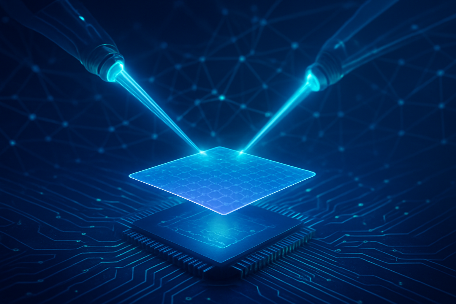
    As of late 2025, the artificial intelligence landscape continues its unprecedented expansion, with semiconductor giants Nvidia (NASDAQ: NVDA) and Broadcom (NASDAQ: AVGO) firmly established as the "AI favorites." These companies, through distinct yet complementary strategies, are not merely supplying components; they are architecting the very infrastructure upon which the global AI revolution is being built. Nvidia dominates the general-purpose AI accelerator market with its comprehensive full-stack ecosystem, while Broadcom excels in custom AI silicon and high-speed networking solutions critical for hyperscale data centers. Their innovations are driving the rapid advancements in AI, from the largest language models to sophisticated autonomous systems, solidifying their indispensable roles in shaping the future of technology.

    The Technical Backbone: Nvidia's Full Stack vs. Broadcom's Specialized Infrastructure

    Both Nvidia and Broadcom are pushing the boundaries of what's technically possible in AI, albeit through different avenues. Their latest offerings showcase significant leaps from previous generations and carve out unique competitive advantages.

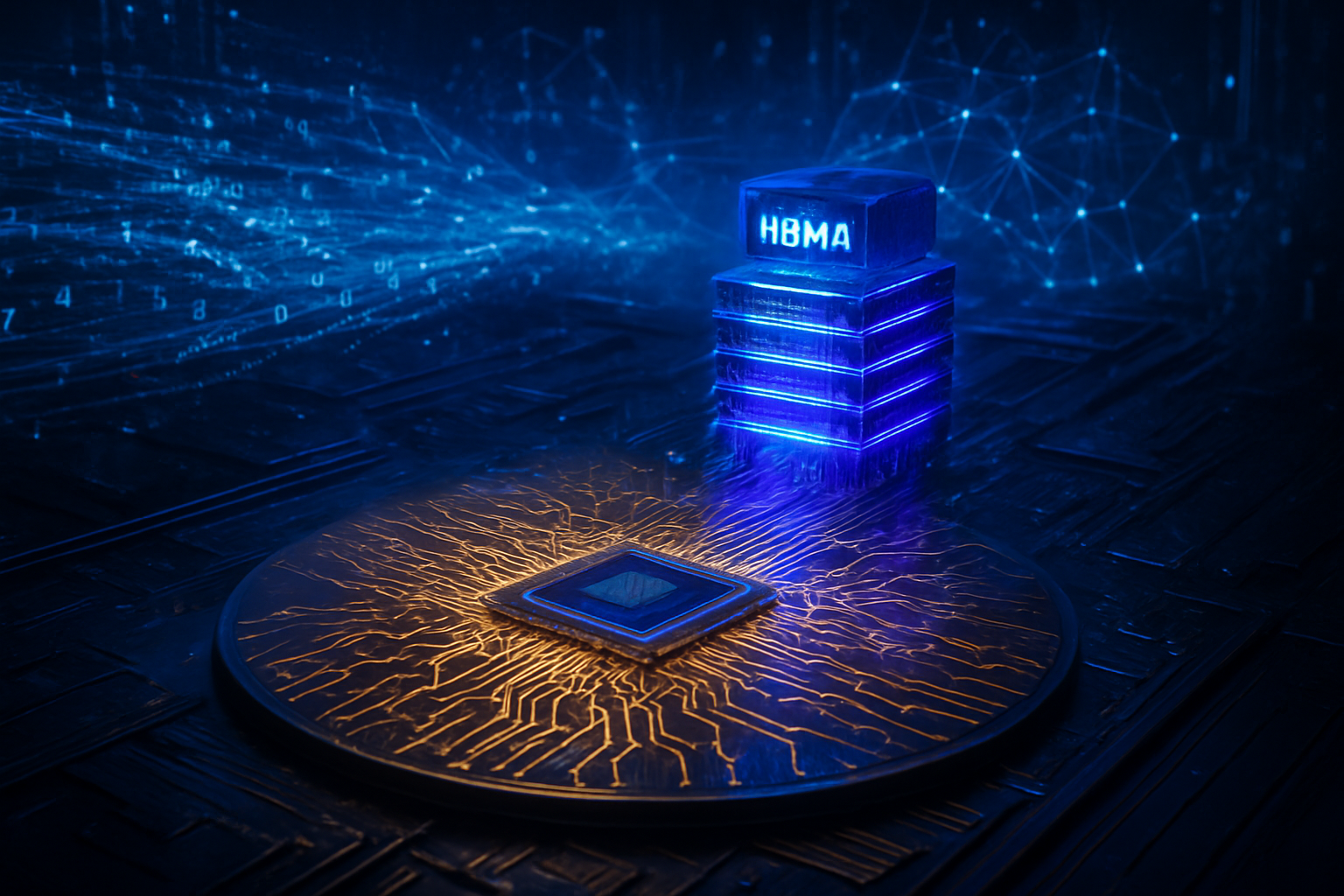
    Nvidia's approach is a full-stack ecosystem, integrating cutting-edge hardware with a robust software platform. At the heart of its hardware innovation is the Blackwell architecture, exemplified by the GB200. Unveiled at GTC 2024, Blackwell represents a revolutionary leap for generative AI, featuring 208 billion transistors and combining two large dies into a unified GPU via a 10 terabit-per-second (TB/s) NVIDIA High-Bandwidth Interface (NV-HBI). It introduces a Second-Generation Transformer Engine with FP4 support, delivering up to 30 times faster real-time trillion-parameter LLM inference and 25 times more energy efficiency than its Hopper predecessor. The Nvidia H200 GPU, an upgrade to the Hopper-architecture H100, focuses on memory and bandwidth, offering 141GB of HBM3e memory and 4.8 TB/s bandwidth, making it ideal for memory-bound AI and HPC workloads. These advancements significantly outpace previous GPU generations by integrating more transistors, higher bandwidth interconnects, and specialized AI processing units.

    Crucially, Nvidia's hardware is underpinned by its CUDA platform. The recent CUDA 13.1 release introduces the "CUDA Tile" programming model, a fundamental shift that abstracts low-level hardware details, simplifying GPU programming and potentially making future CUDA code more portable. This continuous evolution of CUDA, along with libraries like cuDNN and TensorRT, maintains Nvidia's formidable software moat, which competitors like AMD (NASDAQ: AMD) with ROCm and Intel (NASDAQ: INTC) with OpenVINO are striving to bridge. Nvidia's specialized AI software, such as NeMo for generative AI, Omniverse for industrial digital twins, BioNeMo for drug discovery, and the open-source Nemotron 3 family of models, further extends its ecosystem, offering end-to-end solutions that are often lacking in competitor offerings. Initial reactions from the AI community highlight Blackwell as revolutionary and CUDA Tile as the "most substantial advancement" to the platform in two decades, solidifying Nvidia's dominance.

    Broadcom, on the other hand, specializes in highly customized solutions and the critical networking infrastructure for AI. Its custom AI chips (XPUs), such as those co-developed with Google (NASDAQ: GOOGL) for its Tensor Processing Units (TPUs) and Meta (NASDAQ: META) for its MTIA chips, are Application-Specific Integrated Circuits (ASICs) tailored for high-efficiency, low-power AI inference and training. Broadcom's innovative 3.5D eXtreme Dimension System in Package (XDSiP™) platform integrates over 6000 mm² of silicon and up to 12 HBM stacks into a single package, utilizing Face-to-Face (F2F) 3.5D stacking for 7x signal density and 10x power reduction compared to Face-to-Back approaches. This custom silicon offers optimized performance-per-watt and lower Total Cost of Ownership (TCO) for hyperscalers, providing a compelling alternative to general-purpose GPUs for specific workloads.

    Broadcom's high-speed networking solutions are equally vital. The Tomahawk series (e.g., Tomahawk 6, the industry's first 102.4 Tbps Ethernet switch) and Jericho series (e.g., Jericho 4, offering 51.2 Tbps capacity and 3.2 Tbps HyperPort technology) provide the ultra-low-latency, high-throughput interconnects necessary for massive AI compute clusters. The Trident 5-X12 chip even incorporates an on-chip neural-network inference engine, NetGNT, for real-time traffic pattern detection and congestion control. Broadcom's leadership in optical interconnects, including VCSEL, EML, and Co-Packaged Optics (CPO) like the 51.2T Bailly, addresses the need for higher bandwidth and power efficiency over longer distances. These networking advancements are crucial for knitting together thousands of AI accelerators, often providing superior latency and scalability compared to proprietary interconnects like Nvidia's NVLink for large-scale, open Ethernet environments. The AI community recognizes Broadcom as a "foundational enabler" of AI infrastructure, with its custom solutions eroding Nvidia's pricing power and fostering a more competitive market.

    Reshaping the AI Landscape: Impact on Companies and Competitive Dynamics

    The innovations from Nvidia and Broadcom are profoundly reshaping the competitive landscape for AI companies, tech giants, and startups, creating both immense opportunities and significant strategic challenges.

    Nvidia's full-stack AI ecosystem provides a powerful strategic advantage, creating a strong ecosystem lock-in. For AI companies (general), access to Nvidia's powerful GPUs (Blackwell, H200) and comprehensive software (CUDA, NeMo, Omniverse, BioNeMo, Nemotron 3) accelerates development and deployment, lowering the initial barrier to entry for AI innovation. However, the high cost of top-tier Nvidia hardware and potential vendor lock-in remain significant challenges, especially for startups looking to scale rapidly.

    Tech giants like Google (NASDAQ: GOOGL), Microsoft (NASDAQ: MSFT), Meta (NASDAQ: META), and Amazon (NASDAQ: AMZN) are engaged in complex "build vs. buy" decisions. While they continue to rely on Nvidia's GPUs for demanding AI training due to their unmatched performance and mature ecosystem, many are increasingly pursuing a "build" strategy by developing custom AI chips (ASICs/XPUs) to optimize performance, power efficiency, and cost for their specific workloads. This is where Broadcom (NASDAQ: AVGO) becomes a critical partner, supplying components and expertise for these custom solutions, such as Google's TPUs and Meta's MTIA chips. Broadcom's estimated 70% share of the custom AI ASIC market positions it as the clear number two AI compute provider behind Nvidia. This diversification away from general-purpose GPUs can temper Nvidia's long-term pricing power and foster a more competitive market for large-scale, specialized AI deployments.

    Startups benefit from Nvidia's accessible software tools and cloud-based offerings, which can lower the initial barrier to entry for AI development. However, they face intense competition from well-funded tech giants that can afford to invest heavily in both Nvidia's and Broadcom's advanced technologies, or develop their own custom silicon. Broadcom's custom solutions could open niche opportunities for startups specializing in highly optimized, energy-efficient AI applications if they can secure partnerships with hyperscalers or leverage tailored hardware.

    The competitive implications are significant. Nvidia's (NASDAQ: NVDA) market share in AI accelerators (estimated over 80%) remains formidable, driven by its full-stack innovation and ecosystem lock-in. Its integrated platform is positioned as the essential infrastructure for "AI factories." However, Broadcom's (NASDAQ: AVGO) custom silicon offerings enable hyperscalers to reduce reliance on a single vendor and achieve greater control over their AI hardware destiny, leading to potential cost savings and performance optimization for their unique needs. The rapid expansion of the custom silicon market, propelled by Broadcom's collaborations, could challenge Nvidia's traditional GPU sales by 2026, with Broadcom's ASICs offering up to 75% cost savings and 50% lower power consumption for certain workloads. Broadcom's dominance in high-speed Ethernet switches and optical interconnects also makes it indispensable for building the underlying infrastructure of large AI data centers, enabling scalable and efficient AI operations, and benefiting from the shift towards open Ethernet standards over Nvidia's InfiniBand. This dynamic interplay fosters innovation, offers diversified solutions, and signals a future where specialized hardware and integrated, efficient systems will increasingly define success in the AI landscape.

    Broader Significance: AI as the New Industrial Revolution

    The strategies and products of Nvidia and Broadcom signify more than just technological advancements; they represent the foundational pillars of what many are calling the new industrial revolution driven by AI. Their contributions fit into a broader AI landscape characterized by unprecedented scale, specialization, and the pervasive integration of intelligent systems.

    Nvidia's (NASDAQ: NVDA) vision of AI as an "industrial infrastructure," akin to electricity or cloud computing, underscores its foundational role. By pioneering GPU-accelerated computing and establishing the CUDA platform as the industry standard, Nvidia transformed the GPU from a mere graphics processor into the indispensable engine for AI training and complex simulations. This has had a monumental impact on AI development, drastically reducing the time needed to train neural networks and process vast datasets, thereby enabling the development of larger and more complex AI models. Nvidia's full-stack approach, from hardware to software (NeMo, Omniverse), fosters an ecosystem where developers can push the boundaries of AI, leading to breakthroughs in autonomous vehicles, robotics, and medical diagnostics. This echoes the impact of early computing milestones, where foundational hardware and software platforms unlocked entirely new fields of scientific and industrial endeavor.

    Broadcom's (NASDAQ: AVGO) significance lies in enabling the hyperscale deployment and optimization of AI. Its custom ASICs allow major cloud providers to achieve superior efficiency and cost-effectiveness for their massive AI operations, particularly for inference. This specialization is a key trend in the broader AI landscape, moving beyond a "one-size-fits-all" approach with general-purpose GPUs towards workload-specific hardware. Broadcom's high-speed networking solutions are the critical "plumbing" that connect tens of thousands to millions of AI accelerators into unified, efficient computing clusters. This ensures the necessary speed and bandwidth for distributed AI workloads, a scale previously unimaginable. The shift towards specialized hardware, partly driven by Broadcom's success with custom ASICs, parallels historical shifts in computing, such as the move from general-purpose CPUs to GPUs for specific compute-intensive tasks, and even the evolution seen in cryptocurrency mining from GPUs to purpose-built ASICs.

    However, this rapid growth and dominance also raise potential concerns. The significant market concentration, with Nvidia holding an estimated 80-95% market share in AI chips, has led to antitrust investigations and raises questions about vendor lock-in and pricing power. While Broadcom provides a crucial alternative in custom silicon, the overall reliance on a few key suppliers creates supply chain vulnerabilities, exacerbated by intense demand, geopolitical tensions, and export restrictions. Furthermore, the immense energy consumption of AI clusters, powered by these advanced chips, presents a growing environmental and operational challenge. While both companies are working on more energy-efficient designs (e.g., Nvidia's Blackwell platform, Broadcom's co-packaged optics), the sheer scale of AI infrastructure means that overall energy consumption remains a significant concern for sustainability. These concerns necessitate careful consideration as AI continues its exponential growth, ensuring that the benefits of this technological revolution are realized responsibly and equitably.

    The Road Ahead: Future Developments and Expert Predictions

    The future of AI semiconductors, largely charted by Nvidia and Broadcom, promises continued rapid innovation, expanding applications, and evolving market dynamics.

    Nvidia's (NASDAQ: NVDA) near-term developments include the continued rollout of its Blackwell generation GPUs and further enhancements to its CUDA platform. The company is actively launching new AI microservices, particularly targeting vertical markets like healthcare to improve productivity workflows in diagnostics, drug discovery, and digital surgery. Long-term, Nvidia is already developing the next-generation Rubin architecture beyond Blackwell. Its strategy involves evolving beyond just chip design to a more sophisticated business, emphasizing physical AI through robotics and autonomous systems, and agentic AI capable of perceiving, reasoning, planning, and acting autonomously. Nvidia is also exploring deeper integration with advanced memory technologies and engaging in strategic partnerships for next-generation personal computing and 6G development. Experts largely predict Nvidia will remain the dominant force in AI accelerators, with Bank of America projecting significant growth in AI semiconductor sales through 2026, driven by its full-stack approach and deep ecosystem lock-in. However, challenges include potential market saturation by mid-2025 leading to cyclical downturns, intensifying competition in inference, and navigating geopolitical trade policies.

    Broadcom's (NASDAQ: AVGO) near-term focus remains on its custom AI chips (XPUs) and high-speed networking solutions for hyperscale cloud providers. It is transitioning to offering full "system sales," providing integrated racks with multiple components, and leveraging acquisitions like VMware to offer virtualization and cloud infrastructure software with new AI features. Broadcom's significant multi-billion dollar orders for custom ASICs and networking components, including a substantial collaboration with OpenAI for custom AI accelerators and networking systems (deploying from late 2026 to 2029), imply substantial future revenue visibility. Long-term, Broadcom will continue to advance its custom ASIC offerings and optical interconnect solutions (e.g., 1.6-terabit-per-second components) to meet the escalating demands of AI infrastructure. The company aims to strengthen its position as hyperscalers increasingly seek tailored solutions, and to capture a growing share of custom silicon budgets as customers diversify beyond general-purpose GPUs. J.P. Morgan anticipates explosive growth in Broadcom's AI-related semiconductor revenue, projecting it could reach $55-60 billion by fiscal year 2026 and potentially surpass $100 billion by fiscal year 2027. Some experts even predict Broadcom could outperform Nvidia by 2030, particularly as the AI market shifts more towards inference, where custom ASICs can offer greater efficiency.

    Potential applications and use cases on the horizon for both companies are vast. Nvidia's advancements will continue to power breakthroughs in generative AI, autonomous vehicles (NVIDIA DRIVE Hyperion), robotics (Isaac GR00T Blueprint), and scientific computing. Broadcom's infrastructure will be fundamental to scaling these applications in hyperscale data centers, enabling the massive LLMs and proprietary AI stacks of tech giants. The overarching challenges for both companies and the broader industry include ensuring sufficient power availability for data centers, maintaining supply chain resilience amidst geopolitical tensions, and managing the rapid pace of technological innovation. Experts predict a long "AI build-out" phase, spanning 8-10 years, as traditional IT infrastructure is upgraded for accelerated and AI workloads, with a significant shift from AI model training to broader inference becoming a key trend.

    A New Era of Intelligence: Comprehensive Wrap-up

    Nvidia (NASDAQ: NVDA) and Broadcom (NASDAQ: AVGO) stand as the twin titans of the AI semiconductor era, each indispensable in their respective domains, collectively propelling artificial intelligence into its next phase of evolution. Nvidia, with its dominant GPU architectures like Blackwell and its foundational CUDA software platform, has cemented its position as the full-stack leader for AI training and general-purpose acceleration. Its ecosystem, from specialized software like NeMo and Omniverse to open models like Nemotron 3, ensures that it remains the go-to platform for developers pushing the boundaries of AI.

    Broadcom, on the other hand, has strategically carved out a crucial niche as the backbone of hyperscale AI infrastructure. Through its highly customized AI chips (XPUs/ASICs) co-developed with tech giants and its market-leading high-speed networking solutions (Tomahawk, Jericho, optical interconnects), Broadcom enables the efficient and scalable deployment of massive AI clusters. It addresses the critical need for optimized, cost-effective, and power-efficient silicon for inference and the robust "plumbing" that connects millions of accelerators.

    The significance of their contributions cannot be overstated. They are not merely components suppliers but architects of the "AI factory," driving innovation, accelerating development, and reshaping competitive dynamics across the tech industry. While Nvidia's dominance in general-purpose AI is undeniable, Broadcom's rise signifies a crucial trend towards specialization and diversification in AI hardware, offering alternatives that mitigate vendor lock-in and optimize for specific workloads. Challenges remain, including market concentration, supply chain vulnerabilities, and the immense energy consumption of AI infrastructure.

    As we look ahead to the coming weeks and months, watch for continued rapid iteration in GPU architectures and software platforms from Nvidia, further solidifying its ecosystem. For Broadcom, anticipate more significant design wins for custom ASICs with hyperscalers and ongoing advancements in high-speed, power-efficient networking solutions that will underpin the next generation of AI data centers. The complementary strategies of these two giants will continue to define the trajectory of AI, making them essential players to watch in this transformative era.


    This content is intended for informational purposes only and represents analysis of current AI developments.

    TokenRing AI delivers enterprise-grade solutions for multi-agent AI workflow orchestration, AI-powered development tools, and seamless remote collaboration platforms.
    For more information, visit https://www.tokenring.ai/.

  • AI’s Trillion-Dollar Catalyst: Nvidia and Broadcom Soar Amidst Semiconductor Revolution

    AI’s Trillion-Dollar Catalyst: Nvidia and Broadcom Soar Amidst Semiconductor Revolution

    The artificial intelligence revolution has profoundly reshaped the global technology landscape, with its most immediate and dramatic impact felt within the semiconductor industry. As of late 2025, leading chipmakers like Nvidia (NASDAQ: NVDA) and Broadcom (NASDAQ: AVGO) have witnessed unprecedented surges in their market valuations and stock performance, directly fueled by the insatiable demand for the specialized hardware underpinning the AI boom. This surge signifies not just a cyclical upturn but a fundamental revaluation of companies at the forefront of AI infrastructure, presenting both immense opportunities and complex challenges for investors navigating this new era of technological supremacy.

    The AI boom has acted as a powerful catalyst, driving a "giga cycle" of demand and investment within the semiconductor sector. Global semiconductor sales are projected to reach over $800 billion in 2025, with AI-related demand accounting for nearly half of the projected $697 billion sales in 2025. The AI chip market alone is expected to surpass $150 billion in revenue in 2025, a significant increase from $125 billion in 2024. This unprecedented growth underscores the critical role these companies play in enabling the next generation of intelligent technologies, from advanced data centers to autonomous systems.

    The Silicon Engine of AI: From GPUs to Custom ASICs

    The technical backbone of the AI revolution lies in specialized silicon designed for parallel processing and high-speed data handling. At the forefront of this are Nvidia's Graphics Processing Units (GPUs), which have become the de facto standard for training and deploying complex AI models, particularly large language models (LLMs). Nvidia's dominance stems from its CUDA platform, a proprietary parallel computing architecture that allows developers to harness the immense processing power of GPUs for AI workloads. The upcoming Blackwell GPU platform is anticipated to further solidify Nvidia's leadership, offering enhanced performance, efficiency, and scalability crucial for ever-growing AI demands. This differs significantly from previous computing paradigms that relied heavily on general-purpose CPUs, which are less efficient for the highly parallelizable matrix multiplication operations central to neural networks.

    Broadcom, while less visible to the public, has emerged as a "silent winner" through its strategic focus on custom AI chips (XPUs) and high-speed networking solutions. The company's ability to design application-specific integrated circuits (ASICs) tailored to the unique requirements of hyperscale data centers has secured massive contracts with tech giants. For instance, Broadcom's $21 billion deal with Anthropic for Google's custom Ironwood chips highlights its pivotal role in enabling bespoke AI infrastructure. These custom ASICs offer superior power efficiency and performance for specific AI tasks compared to off-the-shelf GPUs, making them highly attractive for companies looking to optimize their vast AI operations. Furthermore, Broadcom's high-bandwidth networking hardware is essential for connecting thousands of these powerful chips within data centers, ensuring seamless data flow that is critical for training and inference at scale.

    The initial reaction from the AI research community and industry experts has been overwhelmingly positive, recognizing the necessity of this specialized hardware to push the boundaries of AI. Researchers are continuously optimizing algorithms to leverage these powerful architectures, while industry leaders are pouring billions into building out the necessary infrastructure.

    Reshaping the Tech Titans: Market Dominance and Strategic Shifts

    The AI boom has profoundly reshaped the competitive landscape for tech giants and startups alike, with semiconductor leaders like Nvidia and Broadcom emerging as indispensable partners. Nvidia, with an estimated 90% market share in AI GPUs, is uniquely positioned. Its chips power everything from cloud-based AI services offered by Amazon (NASDAQ: AMZN) Web Services and Microsoft (NASDAQ: MSFT) Azure to autonomous vehicle platforms and scientific research. This broad penetration gives Nvidia significant leverage and makes it a critical enabler for any company venturing into advanced AI. The company's Data Center division, encompassing most of its AI-related revenue, is expected to double in fiscal 2025 (calendar 2024) to over $100 billion, from $48 billion in fiscal 2024, showcasing its central role.

    Broadcom's strategic advantage lies in its deep partnerships with hyperscalers and its expertise in custom silicon. By developing bespoke AI chips, Broadcom helps these tech giants optimize their AI infrastructure for cost and performance, creating a strong barrier to entry for competitors. While this strategy involves lower-margin custom chip deals, the sheer volume and long-term contracts ensure significant, recurring revenue streams. Broadcom's AI semiconductor revenue increased by 74% year-over-year in its latest quarter, illustrating the success of this approach. This market positioning allows Broadcom to be an embedded, foundational component of the most advanced AI data centers, providing a stable, high-growth revenue base.

    The competitive implications are significant. While Nvidia and Broadcom enjoy dominant positions, rivals like Advanced Micro Devices (NASDAQ: AMD) and Intel (NASDAQ: INTC) are aggressively investing in their own AI chip offerings. AMD's Instinct accelerators are gaining traction, and Intel is pushing its Gaudi series and custom silicon initiatives. Furthermore, the rise of hyperscalers developing in-house AI chips (e.g., Google's TPUs, Amazon's Trainium/Inferentia) poses a potential long-term challenge, though these companies often still rely on external partners for specialized components or manufacturing. This dynamic environment fosters innovation but also demands constant strategic adaptation and technological superiority from the leading players to maintain their competitive edge.

    The Broader AI Canvas: Impacts and Future Horizons

    The current surge in semiconductor demand driven by AI fits squarely into the broader AI landscape as a foundational requirement for continued progress. Without the computational horsepower provided by companies like Nvidia and Broadcom, the sophisticated large language models, advanced computer vision systems, and complex reinforcement learning agents that define today's AI breakthroughs would simply not be possible. This era can be compared to the dot-com boom's infrastructure build-out, but with a more tangible and immediate impact on real-world applications and enterprise solutions. The demand for high-bandwidth memory (HBM), crucial for training LLMs, is projected to grow by 70% in 2025, underscoring the depth of this infrastructure need.

    However, this rapid expansion is not without its concerns. The immense run-up in stock prices and high valuations of leading AI semiconductor companies have fueled discussions about a potential "AI bubble." While underlying demand remains robust, investor scrutiny on profitability, particularly concerning lower-margin custom chip deals (as seen with Broadcom's recent stock dip), highlights a need for sustainable growth strategies. Geopolitical risks, especially the U.S.-China tech rivalry, also continue to influence investments and create potential bottlenecks in the global semiconductor supply chain, adding another layer of complexity.

    Despite these concerns, the wider significance of this period is undeniable. It marks a critical juncture where AI moves beyond theoretical research into widespread practical deployment, necessitating an unprecedented scale of specialized hardware. This infrastructure build-out is as significant as the advent of the internet itself, laying the groundwork for a future where AI permeates nearly every aspect of industry and daily life.

    Charting the Course: Expected Developments and Future Applications

    Looking ahead, the trajectory for AI-driven semiconductor demand remains steeply upward. In the near term, expected developments include the continued refinement of existing AI architectures, with a focus on energy efficiency and specialized capabilities for edge AI applications. Nvidia's Blackwell platform and subsequent generations are anticipated to push performance boundaries even further, while Broadcom will likely expand its portfolio of custom silicon solutions for a wider array of hyperscale and enterprise clients. Analysts expect Nvidia to generate $160 billion from data center sales in 2025, a nearly tenfold increase from 2022, demonstrating the scale of anticipated growth.

    Longer-term, the focus will shift towards more integrated AI systems-on-a-chip (SoCs) that combine processing, memory, and networking into highly optimized packages. Potential applications on the horizon include pervasive AI in robotics, advanced personalized medicine, fully autonomous systems across various industries, and the development of truly intelligent digital assistants that can reason and interact seamlessly. Challenges that need to be addressed include managing the enormous power consumption of AI data centers, ensuring ethical AI development, and diversifying the supply chain to mitigate geopolitical risks. Experts predict that the semiconductor industry will continue to be the primary enabler for these advancements, with innovation in materials science and chip design playing a pivotal role.

    Furthermore, the trend of software-defined hardware will likely intensify, allowing for greater flexibility and optimization of AI workloads on diverse silicon. This will require closer collaboration between chip designers, software developers, and AI researchers to unlock the full potential of future AI systems. The demand for high-bandwidth, low-latency interconnects will also grow exponentially, further benefiting companies like Broadcom that specialize in networking infrastructure.

    A New Era of Silicon: AI's Enduring Legacy

    In summary, the impact of artificial intelligence on leading semiconductor companies like Nvidia and Broadcom has been nothing short of transformative. These firms have not only witnessed their market values soar to unprecedented heights, with Nvidia briefly becoming a $4 trillion company and Broadcom approaching $2 trillion, but they have also become indispensable architects of the global AI infrastructure. Their specialized GPUs, custom ASICs, and high-speed networking solutions are the fundamental building blocks powering the current AI revolution, driving a "giga cycle" of demand that shows no signs of abating.

    This development's significance in AI history cannot be overstated; it marks the transition of AI from a niche academic pursuit to a mainstream technological force, underpinned by a robust and rapidly evolving hardware ecosystem. The ongoing competition from rivals and the rise of in-house chip development by hyperscalers will keep the landscape dynamic, but Nvidia and Broadcom have established formidable leads. Investors, while mindful of high valuations and potential market volatility, continue to view these companies as critical long-term plays in the AI era.

    In the coming weeks and months, watch for continued innovation in chip architectures, strategic partnerships aimed at optimizing AI infrastructure, and the ongoing financial performance of these semiconductor giants as key indicators of the AI industry's health and trajectory.


    This content is intended for informational purposes only and represents analysis of current AI developments.

    TokenRing AI delivers enterprise-grade solutions for multi-agent AI workflow orchestration, AI-powered development tools, and seamless remote collaboration platforms.
    For more information, visit https://www.tokenring.ai/.

  • Broadcom Soars as J.P. Morgan Touts AI Chip Dominance, Projecting Exponential Growth

    Broadcom Soars as J.P. Morgan Touts AI Chip Dominance, Projecting Exponential Growth

    New York, NY – December 16, 2025 – In a significant endorsement reverberating across the semiconductor industry, J.P. Morgan has firmly positioned Broadcom (NASDAQ: AVGO) as a premier chip pick, citing the company's commanding lead in the burgeoning artificial intelligence (AI) chip market as a pivotal growth engine. This bullish outlook, reinforced by recent analyst reports, underscores Broadcom's critical role in powering the next generation of AI infrastructure and its potential for unprecedented revenue expansion in the coming years.

    The investment bank's confidence stems from Broadcom's strategic dominance in custom AI Application-Specific Integrated Circuits (ASICs) and its robust high-performance networking portfolio, both indispensable components for hyperscale data centers and advanced AI workloads. With AI-related revenue projections soaring, J.P. Morgan's analysis, reiterated as recently as December 2025, paints a picture of a company uniquely poised to capitalize on the insatiable demand for AI compute, solidifying its status as a cornerstone of the AI revolution.

    The Architecture of AI Dominance: Broadcom's Technical Edge

    Broadcom's preeminence in the AI chip landscape is deeply rooted in its sophisticated technical offerings, particularly its custom AI chips, often referred to as XPUs, and its high-speed networking solutions. Unlike off-the-shelf general-purpose processors, Broadcom specializes in designing highly customized ASICs tailored for the specific, intensive demands of leading AI developers and cloud providers.

    A prime example of this technical prowess is Broadcom's collaboration with tech giants like Alphabet's Google and Meta Platforms (NASDAQ: META). Broadcom is a key supplier for Google's Tensor Processing Units (TPUs), with J.P. Morgan anticipating substantial revenue contributions from the ongoing ramp-up of Google's TPU v6 (codenamed Ironwood) and future v7 projects. Similarly, Broadcom is instrumental in Meta's Meta Training and Inference Accelerator (MTIA) chip project, powering Meta's vast AI initiatives. This custom ASIC approach allows for unparalleled optimization in terms of performance, power efficiency, and cost for specific AI models and workloads, offering a distinct advantage over more generalized GPU architectures for certain applications. The firm also hinted at early work on an XPU ASIC for a new customer, potentially OpenAI, signaling further expansion of its custom silicon footprint.

    Beyond the custom processors, Broadcom's leadership in high-performance networking is equally critical. The escalating scale of AI models and the distributed nature of AI training and inference demand ultra-fast, low-latency communication within data centers. Broadcom's Tomahawk 5 and upcoming Tomahawk 6 switching chips, along with its Jericho routers, are foundational to these AI clusters. J.P. Morgan highlights the "significant dollar content capture opportunities in scale-up networking," noting that Broadcom offers 5 to 10 times more content in these specialized AI networking environments compared to traditional networking setups, demonstrating a clear technical differentiation and market capture.

    Reshaping the AI Ecosystem: Implications for Tech Giants and Startups

    Broadcom's fortified position in AI chips carries profound implications for the entire AI ecosystem, influencing the competitive dynamics among tech giants, shaping the strategies of AI labs, and even presenting opportunities and challenges for startups. Companies that heavily invest in AI research and deployment, particularly those operating at hyperscale, stand to benefit directly from Broadcom's advanced and efficient custom silicon and networking solutions.

    Hyperscale cloud providers and AI-centric companies like Google and Meta, already leveraging Broadcom's custom XPUs, gain a strategic advantage through optimized hardware that can accelerate their AI development cycles and reduce operational costs associated with massive compute infrastructure. This deep integration allows these tech giants to push the boundaries of AI capabilities, from training larger language models to deploying more sophisticated recommendation engines. For competitors without similar custom silicon partnerships, this could necessitate increased R&D investment in their own chip designs or a reliance on more generic, potentially less optimized, hardware solutions.

    The competitive landscape among major AI labs is also significantly impacted. As the demand for specialized AI hardware intensifies, Broadcom's ability to deliver high-performance, custom solutions becomes a critical differentiator. This could lead to a 'hardware arms race' where access to cutting-edge custom ASICs dictates the pace of AI innovation. For startups, while the direct cost of custom silicon might be prohibitive, the overall improvement in AI infrastructure efficiency driven by Broadcom's technologies could lead to more accessible and powerful cloud-based AI services, fostering innovation by lowering the barrier to entry for complex AI applications. Conversely, startups developing their own AI hardware might face an even steeper climb against the entrenched advantages of Broadcom and its hyperscale partners.

    Broadcom's Role in the Broader AI Landscape and Future Trends

    Broadcom's ascendance in the AI chip sector is not merely a corporate success story but a significant indicator of broader trends within the AI landscape. It underscores a fundamental shift towards specialized hardware as the backbone of advanced AI, moving beyond general-purpose CPUs and even GPUs for specific, high-volume workloads. This specialization allows for unprecedented gains in efficiency and performance, which are crucial as AI models grow exponentially in size and complexity.

    The impact of this trend is multifaceted. It highlights the growing importance of co-design—where hardware and software are developed in tandem—to unlock the full potential of AI. Broadcom's custom ASIC approach is a testament to this, enabling deep optimization that is difficult to achieve with standardized components. This fits into the broader AI trend of "AI factories," where massive compute clusters are purpose-built for continuous AI model training and inference, demanding the kind of high-bandwidth, low-latency networking that Broadcom provides.

    Potential concerns, however, include the increasing concentration of power in the hands of a few chip providers and their hyperscale partners. While custom silicon drives efficiency, it also creates higher barriers to entry for smaller players and could limit hardware diversity in the long run. Comparisons to previous AI milestones, such as the initial breakthroughs driven by GPU acceleration, reveal a similar pattern of hardware innovation enabling new AI capabilities. Broadcom's current trajectory suggests that custom silicon and advanced networking are the next frontier, potentially unlocking AI applications that are currently computationally infeasible.

    The Horizon of AI: Expected Developments and Challenges Ahead

    Looking ahead, Broadcom's trajectory in the AI chip market points to several expected near-term and long-term developments. In the near term, J.P. Morgan anticipates a continued aggressive ramp-up in Broadcom's AI-related semiconductor revenue, projecting a staggering 65% year-over-year increase to approximately $20 billion in fiscal year 2025, with further acceleration to at least $55 billion to $60 billion by fiscal year 2026. Some even suggest it could surpass $100 billion by fiscal year 2027. This growth will be fueled by the ongoing deployment of current-generation custom XPUs and the rapid transition to next-generation platforms like Google's TPU v7.

    Potential applications and use cases on the horizon are vast. As Broadcom continues to innovate with its 2nm 3.5D AI XPU product tape-out on track, it will enable even more powerful and efficient AI models, leading to breakthroughs in areas such as generative AI, autonomous systems, scientific discovery, and personalized medicine. The company is also moving towards providing complete AI rack-level deployment solutions, offering a more integrated and turnkey approach for customers, which could further solidify its market position and value proposition.

    However, challenges remain. The intense competition in the semiconductor space, the escalating costs of advanced chip manufacturing, and the need for continuous innovation to keep pace with rapidly evolving AI algorithms are significant hurdles. Supply chain resilience and geopolitical factors could also impact production and distribution. Experts predict that the demand for specialized AI hardware will only intensify, pushing companies like Broadcom to invest heavily in R&D and forge deeper partnerships with leading AI developers to co-create future solutions. The race for ever-more powerful and efficient AI compute will continue to be a defining characteristic of the tech industry.

    A New Era of AI Compute: Broadcom's Defining Moment

    Broadcom's emergence as a top chip pick for J.P. Morgan, driven by its unparalleled strength in AI chips, marks a defining moment in the history of artificial intelligence. This development is not merely about stock performance; it encapsulates a fundamental shift in how AI is built and scaled. The company's strategic focus on custom AI Application-Specific Integrated Circuits (ASICs) and its leadership in high-performance networking are proving to be indispensable for the hyperscale AI deployments that underpin today's most advanced AI models and services.

    The key takeaway is clear: specialized hardware is becoming the bedrock of advanced AI, and Broadcom is at the forefront of this transformation. Its ability to provide tailored silicon solutions for tech giants like Google and Meta, combined with its robust networking portfolio, creates an "AI Trifecta" that positions it for sustained, exponential growth. This development signifies a maturation of the AI industry, where the pursuit of efficiency and raw computational power demands highly optimized, purpose-built infrastructure.

    In the coming weeks and months, the industry will be watching closely for further updates on Broadcom's custom ASIC projects, especially any new customer engagements like the hinted partnership with OpenAI. The progress of its 2nm 3.5D AI XPU product and its expansion into full AI rack-level solutions will also be crucial indicators of its continued market trajectory. Broadcom's current standing is a testament to its foresight and execution in a rapidly evolving technological landscape, cementing its legacy as a pivotal enabler of the AI-powered future.


    This content is intended for informational purposes only and represents analysis of current AI developments.

    TokenRing AI delivers enterprise-grade solutions for multi-agent AI workflow orchestration, AI-powered development tools, and seamless remote collaboration platforms.
    For more information, visit https://www.tokenring.ai/.

  • Beyond Moore’s Law: Advanced Packaging and Lithography Unleash the Next Wave of AI Performance

    Beyond Moore’s Law: Advanced Packaging and Lithography Unleash the Next Wave of AI Performance

    The relentless pursuit of greater computational power for artificial intelligence is driving a fundamental transformation in semiconductor manufacturing, with advanced packaging and lithography emerging as the twin pillars supporting the next era of AI innovation. As traditional silicon scaling, often referred to as Moore's Law, faces physical and economic limitations, these sophisticated technologies are not merely extending chip capabilities but are indispensable for powering the increasingly complex demands of modern AI, from colossal large language models to pervasive edge computing. Their immediate significance lies in enabling unprecedented levels of performance, efficiency, and integration, fundamentally reshaping the design and production of AI-specific hardware and intensifying the strategic competition within the global tech industry.

    Innovations and Limitations: The Core of AI Semiconductor Evolution

    The AI semiconductor landscape is currently defined by a furious pace of innovation in both advanced packaging and lithography, each addressing critical bottlenecks while simultaneously presenting new challenges. In advanced packaging, the shift towards heterogeneous integration is paramount. Technologies such as 2.5D and 3D stacking, exemplified by Taiwan Semiconductor Manufacturing Company (TSMC) (TPE: 2330)'s CoWoS (Chip-on-Wafer-on-Substrate) variants, allow for the precise placement of multiple dies—including high-bandwidth memory (HBM) and specialized AI accelerators—on a single interposer or stacked vertically. This architecture dramatically reduces data transfer distances, alleviating the "memory wall" bottleneck that has traditionally hampered AI performance by ensuring ultra-fast communication between processing units and memory. Chiplet designs further enhance this modularity, enabling optimized cost and performance by allowing different components to be fabricated on their most suitable process nodes and improving manufacturing yields. Innovations like Intel Corporation (NASDAQ: INTC)'s EMIB (Embedded Multi-die Interconnect Bridge) and emerging Co-Packaged Optics (CPO) for AI networking are pushing the boundaries of integration, promising significant gains in efficiency and bandwidth by the late 2020s.

    However, these advancements come with inherent limitations. The complexity of integrating diverse materials and components in 2.5D and 3D packages introduces significant thermal management challenges, as denser integration generates more heat. The precise alignment required for vertical stacking demands incredibly tight tolerances, increasing manufacturing complexity and potential for defects. Yield management for these multi-die assemblies is also more intricate than for monolithic chips. Initial reactions from the AI research community and industry experts highlight these trade-offs, recognizing the immense performance gains but also emphasizing the need for robust thermal solutions, advanced testing methodologies, and more sophisticated design automation tools to fully realize the potential of these packaging innovations.

    Concurrently, lithography continues its relentless march towards finer features, with Extreme Ultraviolet (EUV) lithography at the forefront. EUV, utilizing 13.5nm wavelength light, enables the fabrication of transistors at 7nm, 5nm, 3nm, and even smaller nodes, which are absolutely critical for the density and efficiency required by modern AI processors. ASML Holding N.V. (NASDAQ: ASML) remains the undisputed leader, holding a near-monopoly on these highly complex and expensive machines. The next frontier is High-NA EUV, with a larger numerical aperture lens (0.55), promising to push feature sizes below 10nm, crucial for future 2nm and 1.4nm nodes like TSMC's A14 process, expected around 2027. While Deep Ultraviolet (DUV) lithography still plays a vital role for less critical layers and memory, the push for leading-edge AI chips is entirely dependent on EUV and its subsequent generations.

    The limitations in lithography primarily revolve around cost, complexity, and the fundamental physics of light. High-NA EUV systems, for instance, are projected to cost around $384 million each, making them an enormous capital expenditure for chip manufacturers. The extreme precision required, the specialized mask infrastructure, and the challenges of defect control at such minuscule scales contribute to significant manufacturing hurdles and impact overall yields. Emerging technologies like X-ray lithography (XRL) and nanoimprint lithography are being explored as potential long-term solutions to overcome some of these inherent limitations and to avoid the need for costly multi-patterning techniques at future nodes. Furthermore, AI itself is increasingly being leveraged within lithography processes, optimizing mask designs, predicting defects, and refining process parameters to improve efficiency and yield, demonstrating a symbiotic relationship between AI development and the tools that enable it.

    The Shifting Sands of AI Supremacy: Who Benefits from the Packaging and Lithography Revolution

    The advancements in advanced packaging and lithography are not merely technical feats; they are profound strategic enablers, fundamentally reshaping the competitive landscape for AI companies, tech giants, and burgeoning startups alike. At the forefront of benefiting are the major semiconductor foundries and Integrated Device Manufacturers (IDMs) like Taiwan Semiconductor Manufacturing Company (TSMC) (TPE: 2330), Intel Corporation (NASDAQ: INTC), and Samsung Electronics Co., Ltd. (KRX: 005930). TSMC's dominance in advanced packaging technologies such as CoWoS and InFO makes it an indispensable partner for virtually all leading AI chip designers. Similarly, Intel's EMIB and Foveros, and Samsung's I-Cube, are critical offerings that allow these giants to integrate diverse components into high-performance packages, solidifying their positions as foundational players in the AI supply chain. Their massive investments in expanding advanced packaging capacity underscore its strategic importance.

    AI chip designers and accelerator developers are also significant beneficiaries. NVIDIA Corporation (NASDAQ: NVDA), the undisputed leader in AI GPUs, heavily leverages 2.5D and 3D stacking with High Bandwidth Memory (HBM) for its cutting-edge accelerators like the H100, maintaining its competitive edge. Advanced Micro Devices, Inc. (NASDAQ: AMD) is a strong challenger, utilizing similar packaging strategies for its MI300 series. Hyperscalers and tech giants like Alphabet Inc. (Google) (NASDAQ: GOOGL) with its TPUs and Amazon.com, Inc. (NASDAQ: AMZN) with its Graviton and Trainium chips are increasingly relying on custom silicon, optimized through advanced packaging, to achieve superior performance-per-watt and cost efficiency for their vast AI workloads. This trend signals a broader move towards vertical integration where software, silicon, and packaging are co-designed for maximum impact.

    The competitive implications are stark. Advanced packaging has transcended its traditional role as a back-end process to become a core architectural enabler and a strategic differentiator. Companies with robust R&D and manufacturing capabilities in these areas gain substantial advantages, while those lagging risk being outmaneuvered. The shift towards modular, chiplet-based architectures, facilitated by advanced packaging, is a significant disruption. It allows for greater flexibility and could, to some extent, democratize chip design by enabling smaller startups to innovate by integrating specialized chiplets without the prohibitively high cost of designing an entire System-on-a-Chip (SoC) from scratch. However, this also introduces new challenges around chiplet interoperability and standardization. The "memory wall" – the bottleneck in data transfer between processing units and memory – is directly addressed by advanced packaging, which is crucial for the performance of large language models and generative AI.

    Market positioning is increasingly defined by access to and expertise in these advanced technologies. ASML Holding N.V. (NASDAQ: ASML), as the sole provider of leading-edge EUV lithography systems, holds an unparalleled strategic advantage, making it one of the most critical companies in the entire semiconductor ecosystem. Memory manufacturers like SK Hynix Inc. (KRX: 000660), Micron Technology, Inc. (NASDAQ: MU), and Samsung are experiencing surging demand for HBM, essential for high-performance AI accelerators. Outsourced Semiconductor Assembly and Test (OSAT) providers such as ASE Technology Holding Co., Ltd. (NYSE: ASX) and Amkor Technology, Inc. (NASDAQ: AMKR) are also becoming indispensable partners in the complex assembly of these advanced packages. Ultimately, the ability to rapidly innovate and scale production of AI chips through advanced packaging and lithography is now a direct determinant of strategic advantage and market leadership in the fiercely competitive AI race.

    A New Foundation for AI: Broader Implications and Looming Concerns

    The current revolution in advanced packaging and lithography is far more than an incremental improvement; it represents a foundational shift that is profoundly impacting the broader AI landscape and shaping its future trajectory. These hardware innovations are the essential bedrock upon which the next generation of AI systems, particularly the resource-intensive large language models (LLMs) and generative AI, are being built. By enabling unprecedented levels of performance, efficiency, and integration, they allow for the realization of increasingly complex neural network architectures and greater computational density, pushing the boundaries of what AI can achieve. This scaling is critical for everything from hyperscale data centers powering global AI services to compact, energy-efficient AI at the edge in devices and autonomous systems.

    This era of hardware innovation fits into the broader AI trend of moving beyond purely algorithmic breakthroughs to a symbiotic relationship between software and silicon. While previous AI milestones, such as the advent of deep learning algorithms or the widespread adoption of GPUs for parallel processing, were primarily driven by software and architectural insights, advanced packaging and lithography provide the physical infrastructure necessary to scale and deploy these innovations efficiently. They are directly addressing the "memory wall" bottleneck, a long-standing limitation in AI accelerator performance, by placing memory closer to processing units, leading to faster data access, higher bandwidth, and lower latency—all critical for the data-hungry demands of modern AI. This marks a departure from reliance solely on Moore's Law, as packaging has transitioned from a supportive back-end process to a core architectural enabler, integrating diverse chiplets and components into sophisticated "mini-systems."

    However, this transformative period is not without its concerns. The primary challenges revolve around the escalating cost and complexity of these advanced manufacturing processes. Designing, manufacturing, and testing 2.5D/3D stacked chips and chiplet systems are significantly more complex and expensive than traditional monolithic designs, leading to increased development costs and longer design cycles. The exorbitant price of High-NA EUV tools, for instance, translates into higher wafer costs. Thermal management is another critical issue; denser integration in advanced packages generates more localized heat, demanding innovative and robust cooling solutions to prevent performance degradation and ensure reliability.

    Perhaps the most pressing concern is the bottleneck in advanced packaging capacity. Technologies like TSMC's CoWoS are in such high demand that hyperscalers are pre-booking capacity up to eighteen months in advance, leaving smaller startups struggling to secure scarce slots and often facing idle wafers awaiting packaging. This capacity crunch can stifle innovation and slow the deployment of new AI technologies. Furthermore, geopolitical implications are significant, with export restrictions on advanced lithography machines to certain countries (e.g., China) creating substantial tensions and impacting their ability to produce cutting-edge AI chips. The environmental impact also looms large, as these advanced manufacturing processes become more energy-intensive and resource-demanding. Some experts even predict that the escalating demand for AI training could, in a decade or so, lead to power consumption exceeding globally available power, underscoring the urgent need for even more efficient models and hardware.

    The Horizon of AI Hardware: Future Developments and Expert Predictions

    The trajectory of advanced packaging and lithography points towards an even more integrated and specialized future for AI semiconductors. In the near-term, we can expect a continued rapid expansion of 2.5D and 3D integration, with a focus on improving hybrid bonding techniques to achieve even finer interconnect pitches and higher stack densities. The widespread adoption of chiplet architectures will accelerate, driven by the need for modularity, cost-effectiveness, and the ability to mix-and-match specialized components from different process nodes. This will necessitate greater standardization in chiplet interfaces and communication protocols to foster a more open and interoperable ecosystem. The commercialization and broader deployment of High-NA EUV lithography, particularly for sub-2nm process nodes, will be a critical near-term development, enabling the next generation of ultra-dense transistors.

    Looking further ahead, long-term developments include the exploration of novel materials and entirely new integration paradigms. Co-Packaged Optics (CPO) will likely become more prevalent, integrating optical interconnects directly into advanced packages to overcome electrical bandwidth limitations for inter-chip and inter-system communication, crucial for exascale AI systems. Experts predict the emergence of "system-on-wafer" or "system-in-package" solutions that blur the lines between chip and system, creating highly integrated, application-specific AI engines. Research into alternative lithography methods like X-ray lithography and nanoimprint lithography could offer pathways beyond the physical limits of current EUV technology, potentially enabling even finer features without the complexities of multi-patterning.

    The potential applications and use cases on the horizon are vast. More powerful and efficient AI chips will enable truly ubiquitous AI, powering highly autonomous vehicles with real-time decision-making capabilities, advanced personalized medicine through rapid genomic analysis, and sophisticated real-time simulation and digital twin technologies. Generative AI models will become even larger and more capable, moving beyond text and images to create entire virtual worlds and complex interactive experiences. Edge AI devices, from smart sensors to robotics, will gain unprecedented processing power, enabling complex AI tasks locally without constant cloud connectivity, enhancing privacy and reducing latency.

    However, several challenges need to be addressed to fully realize this future. Beyond the aforementioned cost and thermal management issues, the industry must tackle the growing complexity of design and verification for these highly integrated systems. New Electronic Design Automation (EDA) tools and methodologies will be essential. Supply chain resilience and diversification will remain critical, especially given geopolitical tensions. Furthermore, the energy consumption of AI training and inference, already a concern, will demand continued innovation in energy-efficient hardware architectures and algorithms to ensure sustainability. Experts predict a future where hardware and software co-design becomes even more intertwined, with AI itself playing a crucial role in optimizing chip design, manufacturing processes, and even material discovery. The industry is moving towards a holistic approach where every layer of the technology stack, from atoms to algorithms, is optimized for AI.

    The Indispensable Foundation: A Wrap-up on AI's Hardware Revolution

    The advancements in advanced packaging and lithography are not merely technical footnotes in the story of AI; they are the bedrock upon which the future of artificial intelligence is being constructed. The key takeaway is clear: as traditional methods of scaling transistor density reach their physical and economic limits, these sophisticated hardware innovations have become indispensable for continuing the exponential growth in computational power required by modern AI. They are enabling heterogeneous integration, alleviating the "memory wall" with High Bandwidth Memory, and pushing the boundaries of miniaturization with Extreme Ultraviolet lithography, thereby unlocking unprecedented performance and efficiency for everything from generative AI to edge computing.

    This development marks a pivotal moment in AI history, akin to the introduction of the GPU for parallel processing or the breakthroughs in deep learning algorithms. Unlike those milestones, which were largely software or architectural, advanced packaging and lithography provide the fundamental physical infrastructure that allows these algorithmic and architectural innovations to be realized at scale. They represent a strategic shift where the "back-end" of chip manufacturing has become a "front-end" differentiator, profoundly impacting competitive dynamics among tech giants, fostering new opportunities for innovation, and presenting significant challenges related to cost, complexity, and supply chain bottlenecks.

    The long-term impact will be a world increasingly permeated by intelligent systems, powered by chips that are more integrated, specialized, and efficient than ever before. This hardware revolution will enable AI to tackle problems of greater complexity, operate with higher autonomy, and integrate seamlessly into every facet of our lives. In the coming weeks and months, we should watch for continued announcements regarding expanded advanced packaging capacity from leading foundries, further refinements in High-NA EUV deployment, and the emergence of new chiplet standards. The race for AI supremacy will increasingly be fought not just in algorithms and data, but in the very atoms and architectures that form the foundation of intelligent machines.


    This content is intended for informational purposes only and represents analysis of current AI developments.

    TokenRing AI delivers enterprise-grade solutions for multi-agent AI workflow orchestration, AI-powered development tools, and seamless remote collaboration platforms.
    For more information, visit https://www.tokenring.ai/.