Tag: AI Hardware

  • Beyond Silicon: How Advanced Materials and 3D Packaging Are Revolutionizing AI Chips

    Beyond Silicon: How Advanced Materials and 3D Packaging Are Revolutionizing AI Chips

    The insatiable demand for ever-increasing computational power and efficiency in Artificial Intelligence (AI) applications is pushing the boundaries of traditional silicon-based semiconductor manufacturing. As the industry grapples with the physical limits of transistor scaling, a new era of innovation is dawning, driven by groundbreaking advancements in semiconductor materials and sophisticated advanced packaging techniques. These emerging technologies, including 3D packaging, chiplets, and hybrid bonding, are not merely incremental improvements; they represent a fundamental shift in how AI chips are designed and fabricated, promising unprecedented levels of performance, power efficiency, and functionality.

    These innovations are critical for powering the next generation of AI, from colossal large language models (LLMs) in hyperscale data centers to compact, energy-efficient AI at the edge. By enabling denser integration, faster data transfer, and superior thermal management, these advancements are poised to accelerate AI development, unlock new capabilities, and reshape the competitive landscape of the global technology industry. The convergence of novel materials and advanced packaging is set to be the cornerstone of future AI breakthroughs, addressing bottlenecks that traditional methods can no longer overcome.

    The Architectural Revolution: 3D Stacking, Chiplets, and Hybrid Bonding Unleashed

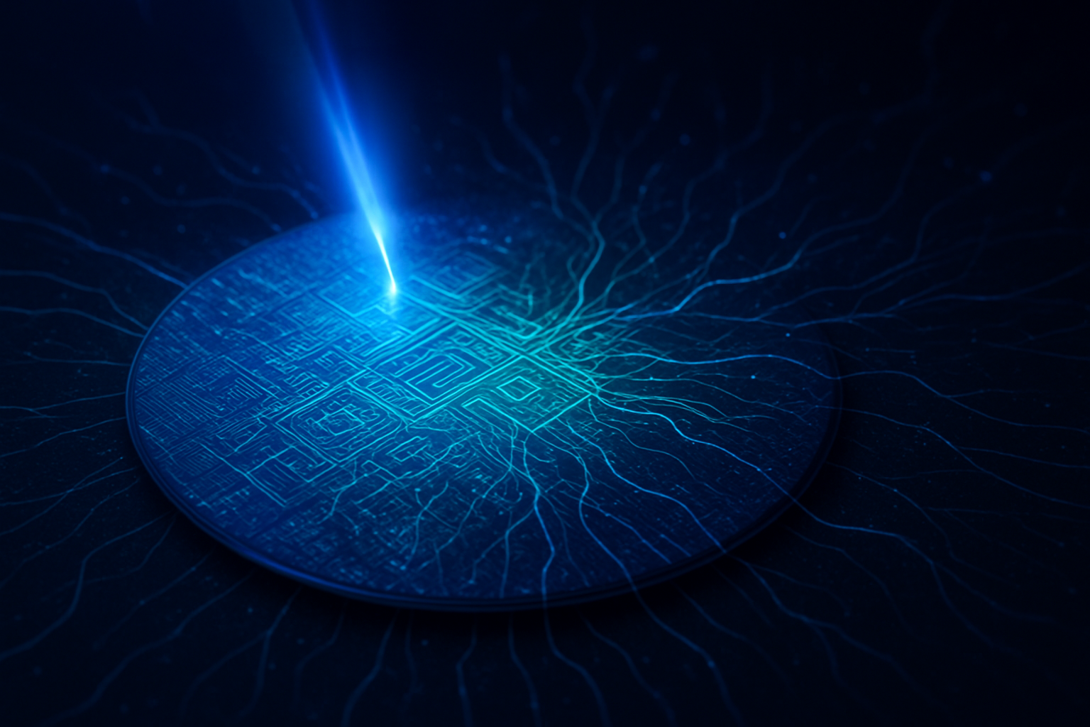
    The core of this revolution lies in moving beyond the flat, monolithic chip design to a three-dimensional, modular architecture. This paradigm shift involves several key technical advancements that work in concert to enhance AI chip performance and efficiency dramatically.

    3D Packaging, encompassing 2.5D and true vertical stacking, is at the forefront. Instead of placing components side-by-side on a large, expensive silicon die, chips are stacked vertically, drastically shortening the physical distance data must travel between compute units and memory. This directly translates to vastly increased memory bandwidth and significantly reduced latency – two critical factors for AI workloads, which are often memory-bound and require rapid access to massive datasets. Companies like TSMC (NYSE: TSM) are leaders in this space with their CoWoS (Chip-on-Wafer-on-Substrate) technology, a 2.5D packaging solution widely adopted for high-performance AI accelerators such as NVIDIA's (NASDAQ: NVDA) H100. Intel (NASDAQ: INTC) is also heavily invested with Foveros (3D stacking) and EMIB (Embedded Multi-die Interconnect Bridge), while Samsung (KRX: 005930) offers I-Cube (2.5D) and X-Cube (3D stacking) platforms.

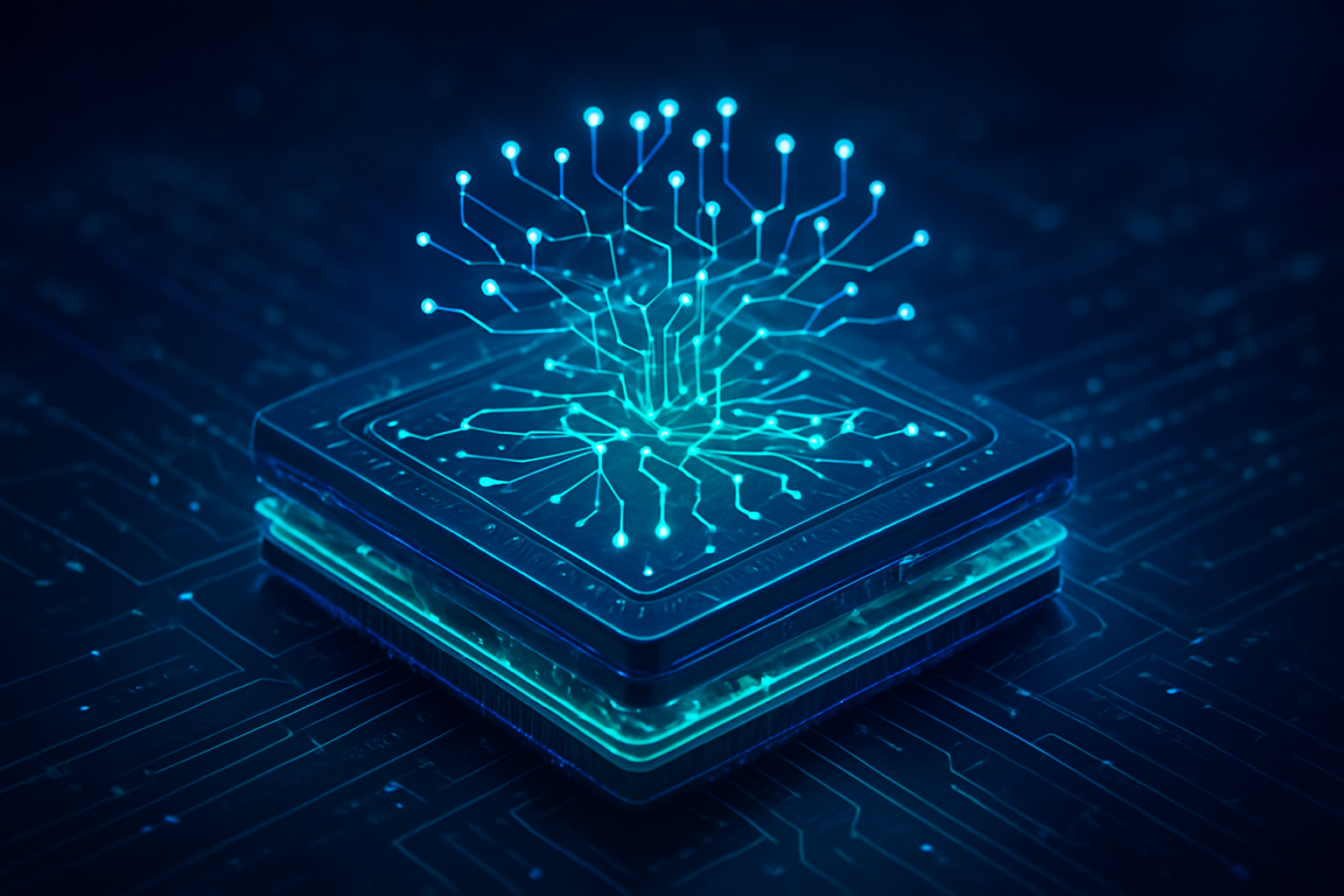
    Complementing 3D packaging are Chiplets, a modular design approach where a complex System-on-Chip (SoC) is disaggregated into smaller, specialized "chiplets" (e.g., CPU, GPU, memory, I/O, AI accelerators). These chiplets are then integrated into a single package using advanced packaging techniques. This offers unparalleled flexibility, allowing designers to mix and match different chiplets, each manufactured on the most optimal (and cost-effective) process node for its specific function. This heterogeneous integration is particularly beneficial for AI, enabling the creation of highly customized accelerators tailored for specific workloads. AMD (NASDAQ: AMD) has been a pioneer in this area, utilizing chiplets with 3D V-cache in its Ryzen processors and integrating CPU/GPU tiles in its Instinct MI300 series.

    The glue that binds these advanced architectures together is Hybrid Bonding. This cutting-edge direct copper-to-copper (Cu-Cu) bonding technology creates ultra-dense vertical interconnections between dies or wafers at pitches below 10 µm, even approaching sub-micron levels. Unlike traditional methods that rely on solder or intermediate materials, hybrid bonding forms direct metal-to-metal connections, dramatically increasing I/O density and bandwidth while minimizing parasitic capacitance and resistance. This leads to lower latency, reduced power consumption, and improved thermal conduction, all vital for the demanding power and thermal requirements of AI chips. IBM Research and ASMPT have achieved significant milestones, pushing interconnection sizes to around 0.8 microns, enabling over 1000 GB/s bandwidth with high energy efficiency.

    These advancements represent a significant departure from the monolithic chip design philosophy. Previous approaches focused primarily on shrinking transistors on a single die (Moore's Law). While transistor scaling remains important, advanced packaging and chiplets offer a new dimension of performance scaling by optimizing inter-chip communication and allowing for heterogeneous integration. The initial reactions from the AI research community and industry experts are overwhelmingly positive, recognizing these techniques as essential for sustaining the pace of AI innovation. They are seen as crucial for breaking the "memory wall" and enabling the power-efficient processing required for increasingly complex AI models.

    Reshaping the AI Competitive Landscape

    These emerging trends in semiconductor materials and advanced packaging are poised to profoundly impact AI companies, tech giants, and startups alike, creating new competitive dynamics and strategic advantages.

    NVIDIA (NASDAQ: NVDA), a dominant player in AI hardware, stands to benefit immensely. Their cutting-edge GPUs, like the H100, already leverage TSMC's CoWoS 2.5D packaging to integrate the GPU die with high-bandwidth memory (HBM). As 3D stacking and hybrid bonding become more prevalent, NVIDIA can further optimize its accelerators for even greater performance and efficiency, maintaining its lead in the AI training and inference markets. The ability to integrate more specialized AI acceleration chiplets will be key.

    Intel (NASDAQ: INTC), is strategically positioning itself to regain market share in the AI space through its robust investments in advanced packaging technologies like Foveros and EMIB. By leveraging these capabilities, Intel aims to offer highly competitive AI accelerators and CPUs that integrate diverse computing elements, challenging NVIDIA and AMD. Their foundry services, offering these advanced packaging options to third parties, could also become a significant revenue stream and influence the broader ecosystem.

    AMD (NASDAQ: AMD) has already demonstrated its prowess with chiplet-based designs in its CPUs and GPUs, particularly with its Instinct MI300 series, which combines CPU and GPU elements with HBM using advanced packaging. Their early adoption and expertise in chiplets give them a strong competitive edge, allowing for flexible, cost-effective, and high-performance solutions tailored for various AI workloads.

    Foundries like TSMC (NYSE: TSM) and Samsung (KRX: 005930) are critical enablers. Their continuous innovation and expansion of advanced packaging capacities are essential for the entire AI industry. Their ability to provide cutting-edge packaging services will determine who can bring the most performant and efficient AI chips to market. The competition between these foundries to offer the most advanced 2.5D/3D integration and hybrid bonding capabilities will be fierce.

    Beyond the major chip designers, companies specializing in advanced materials like Wolfspeed (NYSE: WOLF), Infineon (FSE: IFX), and Navitas Semiconductor (NASDAQ: NVTS) are becoming increasingly vital. Their wide-bandgap materials (SiC and GaN) are crucial for power management in AI data centers, where power efficiency is paramount. Startups focusing on novel 2D materials or specialized chiplet designs could also find niches, offering custom solutions for emerging AI applications.

    The potential disruption to existing products and services is significant. Monolithic chip designs will increasingly struggle to compete with the performance and efficiency offered by advanced packaging and chiplets, particularly for demanding AI tasks. Companies that fail to adopt these architectural shifts risk falling behind. Market positioning will increasingly depend not just on transistor technology but also on expertise in heterogeneous integration, thermal management, and robust supply chains for advanced packaging.

    Wider Significance and Broad AI Impact

    These advancements in semiconductor materials and advanced packaging are more than just technical marvels; they represent a pivotal moment in the broader AI landscape, addressing fundamental limitations and paving the way for unprecedented capabilities.

    Foremost, these innovations are directly addressing the slowdown of Moore's Law. While transistor density continues to increase, the rate of performance improvement per dollar has decelerated. Advanced packaging offers a "More than Moore" solution, providing performance gains by optimizing inter-component communication and integration rather than solely relying on transistor shrinks. This allows for continued progress in AI chip capabilities even as the physical limits of silicon are approached.

    The impact on AI development is profound. The ability to integrate high-bandwidth memory directly with compute units in 3D stacks, enabled by hybrid bonding, is crucial for training and deploying increasingly massive AI models, such as large language models (LLMs) and complex generative AI architectures. These models demand vast amounts of data to be moved quickly between processors and memory, a bottleneck that traditional packaging struggles to overcome. Enhanced power efficiency from wide-bandgap materials and optimized chip designs also makes AI more sustainable and cost-effective to operate at scale.

    Potential concerns, however, are not negligible. The complexity of designing, manufacturing, and testing 3D stacked chips and chiplet systems is significantly higher than monolithic designs. This can lead to increased development costs, longer design cycles, and new challenges in thermal management, as stacking chips generates more localized heat. Supply chain complexities also multiply, requiring tighter collaboration between chip designers, foundries, and outsourced assembly and test (OSAT) providers. The cost of advanced packaging itself can be substantial, potentially limiting its initial adoption to high-end AI applications.

    Comparing this to previous AI milestones, this architectural shift is as significant as the advent of GPUs for parallel processing or the development of specialized AI accelerators like TPUs. It's a foundational change that enables the next wave of algorithmic breakthroughs by providing the necessary hardware substrate. It moves beyond incremental improvements to a systemic rethinking of chip design, akin to the transition from single-core to multi-core processors, but with an added dimension of vertical integration and modularity.

    The Road Ahead: Future Developments and Challenges

    The trajectory for these emerging trends points towards even more sophisticated integration and specialized materials, with significant implications for future AI applications.

    In the near term, we can expect to see wider adoption of 2.5D and 3D packaging across a broader range of AI accelerators, moving beyond just the highest-end data center chips. Hybrid bonding will become increasingly common for integrating memory and compute, pushing interconnect densities even further. The UCIe (Universal Chiplet Interconnect Express) standard will gain traction, fostering a more open and interoperable chiplet ecosystem, allowing companies to mix and match chiplets from different vendors. This will drive down costs and accelerate innovation by democratizing access to specialized IP.

    Long-term developments include the deeper integration of novel materials. While 2D materials like graphene and molybdenum disulfide are still primarily in research, breakthroughs in fabricating semiconducting graphene with useful bandgaps suggest future possibilities for ultra-thin, high-mobility transistors that could be heterogeneously integrated with silicon. Silicon Carbide (SiC) and Gallium Nitride (GaN) will continue to mature, not just for power electronics but potentially for high-frequency AI processing at the edge, enabling extremely compact and efficient AI devices for IoT and mobile applications. We might also see the integration of optical interconnects within 3D packages to further reduce latency and increase bandwidth for inter-chiplet communication.

    Challenges remain formidable. Thermal management in densely packed 3D stacks is a critical hurdle, requiring innovative cooling solutions and thermal interface materials. Ensuring manufacturing yield and reliability for complex multi-chiplet, 3D stacked systems is another significant engineering task. Furthermore, the development of robust design tools and methodologies that can efficiently handle the complexities of heterogeneous integration and 3D layout is essential.

    Experts predict that the future of AI hardware will be defined by highly specialized, heterogeneously integrated systems, meticulously optimized for specific AI workloads. This will move away from general-purpose computing towards purpose-built AI engines. The emphasis will be on system-level performance, power efficiency, and cost-effectiveness, with packaging becoming as important as the transistors themselves. What experts predict is a future where AI accelerators are not just faster, but also smarter in how they manage and move data, driven by these architectural and material innovations.

    A New Era for AI Hardware

    The convergence of emerging semiconductor materials and advanced packaging techniques marks a transformative period for AI hardware. The shift from monolithic silicon to modular, three-dimensional architectures utilizing chiplets, 3D stacking, and hybrid bonding, alongside the exploration of wide-bandgap and 2D materials, is fundamentally reshaping the capabilities of AI chips. These innovations are critical for overcoming the limitations of traditional transistor scaling, providing the unprecedented bandwidth, lower latency, and improved power efficiency demanded by today's and tomorrow's sophisticated AI models.

    The significance of this development in AI history cannot be overstated. It is a foundational change that enables the continued exponential growth of AI capabilities, much like the invention of the transistor itself or the advent of parallel computing with GPUs. It signifies a move towards a more holistic, system-level approach to chip design, where packaging is no longer a mere enclosure but an active component in enhancing performance.

    In the coming weeks and months, watch for continued announcements from major foundries and chip designers regarding expanded advanced packaging capacities and new product launches leveraging these technologies. Pay close attention to the development of open chiplet standards and the increasing adoption of hybrid bonding in commercial products. The success in tackling thermal management and manufacturing complexity will be key indicators of how rapidly these advancements proliferate across the AI ecosystem. This architectural revolution is not just about building faster chips; it's about building the intelligent infrastructure for the future of AI.


    This content is intended for informational purposes only and represents analysis of current AI developments.

    TokenRing AI delivers enterprise-grade solutions for multi-agent AI workflow orchestration, AI-powered development tools, and seamless remote collaboration platforms.
    For more information, visit https://www.tokenring.ai/.

  • Unlocking AI’s Full Potential: ASML’s EUV Lithography Becomes the Indispensable Foundation for Next-Gen Chips

    Unlocking AI’s Full Potential: ASML’s EUV Lithography Becomes the Indispensable Foundation for Next-Gen Chips

    The exponential growth of Artificial Intelligence (AI) and its insatiable demand for processing power have rendered traditional chip manufacturing methods inadequate, thrusting ASML's (AMS: ASML) Extreme Ultraviolet (EUV) lithography technology into an immediately critical and indispensable role. This groundbreaking technology, in which ASML holds a global monopoly, uses ultra-short 13.5-nanometer wavelengths of light to etch incredibly intricate patterns onto silicon wafers, enabling the creation of microchips with billions of smaller, more densely packed transistors.

    This unparalleled precision is the bedrock upon which next-generation AI accelerators, data center GPUs, and sophisticated edge AI solutions are built, providing the enhanced processing capabilities and vital energy efficiency required to power the most advanced AI applications today and in the immediate future. Without ASML's EUV systems, the semiconductor industry would face a significant barrier to scaling chip performance, making the continued advancement and real-world deployment of cutting-edge AI heavily reliant on this singular technological marvel.

    The Microscopic Marvel: Technical Deep Dive into EUV's Edge

    ASML's Extreme Ultraviolet (EUV) lithography technology represents a monumental leap in semiconductor manufacturing, enabling the creation of microchips with unprecedented density and performance. This intricate process is crucial for sustaining Moore's Law and powering the latest advancements in artificial intelligence (AI), high-performance computing, and other cutting-edge technologies. ASML is currently the sole supplier of EUV lithography systems globally.

    At the core of ASML's EUV technology is the use of light with an extremely short wavelength of 13.5 nanometers (nm), which is nearly in the X-ray range and more than 14 times shorter than the 193 nm wavelength used in previous Deep Ultraviolet (DUV) systems. This ultra-short wavelength is fundamental to achieving finer resolution and printing smaller features on silicon wafers. Key technical specifications include EUV light generated by firing two separate CO2 laser pulses at microscopic droplets of molten tin 50,000 times per second. Unlike DUV systems that use refractive lenses, EUV light is absorbed by nearly all materials, necessitating operation in a vacuum chamber and the use of highly specialized multi-layer mirrors, developed in collaboration with companies like Carl Zeiss SMT, to guide and focus the light. These mirrors are so precise that if scaled to the size of a country, the largest imperfection would be only about 1 millimeter.

    Current generation NXE systems (e.g., NXE:3400C, NXE:3600D) have a numerical aperture of 0.33, enabling them to print features with a resolution of 13 nm, supporting volume production for 7 nm, 5 nm, and 3 nm logic nodes. The next-generation platform, High-NA EUV (EXE platform, e.g., TWINSCAN EXE:5000, EXE:5200B), significantly increases the numerical aperture to 0.55, improving resolution to just 8 nm. This allows for transistors that are 1.7 times smaller and transistor densities 2.9 times higher. The first High-NA EUV system was delivered in December 2023, with high-volume manufacturing expected between 2025 and 2026 for advanced nodes starting at 2 nm logic. High-NA EUV systems are designed for higher productivity, with initial capabilities of printing over 185 wafers per hour (wph).

    The transition from Deep Ultraviolet (DUV) to Extreme Ultraviolet (EUV) lithography marks a fundamental shift. The most significant difference is the light wavelength—13.5 nm for EUV compared to 193 nm for DUV. DUV systems use refractive lenses and can operate in air, while EUV necessitates an entirely reflective optical system within a vacuum. EUV can achieve much smaller feature sizes, enabling advanced nodes where DUV lithography typically hits its limit around 40-20 nm without complex resolution enhancement techniques like multi-patterning, which EUV often simplifies into a single pass. The AI research community and industry experts have expressed overwhelmingly positive reactions, recognizing EUV's indispensable role in sustaining Moore's Law and enabling the fabrication of the ever-smaller, more powerful, and energy-efficient chips required for the exponential growth in AI, quantum computing, and other advanced technologies.

    Reshaping the AI Battleground: Corporate Beneficiaries and Competitive Edge

    ASML's EUV lithography technology is a pivotal enabler for the advancement of artificial intelligence, profoundly impacting AI companies, tech giants, and startups by shaping the capabilities, costs, and competitive landscape of advanced chip manufacturing. It is critical for producing the advanced semiconductors that power AI systems, allowing for higher transistor densities, increased processing capabilities, and lower power consumption in AI chips. This is essential for scaling semiconductor devices to 7nm, 5nm, 3nm, and even sub-2nm nodes, which are vital for developing specialized AI accelerators and neural processing units.

    The companies that design and manufacture the most advanced AI chips are the primary beneficiaries of ASML's EUV technology. TSMC (NYSE: TSM), as the world's largest contract chipmaker, is a leading implementer of EUV, extensively integrating it into its fabrication processes for nodes such as N7+, N5, N3, and the upcoming N2. TSMC received its first High-NA (High Numerical Aperture) EUV machine in September 2024, signaling its commitment to maintaining leadership in advanced AI chip manufacturing, with plans to integrate it into its A14 (1.4nm) process node by 2027. Samsung Electronics (KRX: 005930) is another key player heavily investing in EUV, planning to deploy High-NA EUV at its 2nm node, potentially ahead of TSMC's 1.4nm timeline, with a significant investment in two of ASML’s EXE:5200B High-NA EUV tools. Intel (NASDAQ: INTC) is actively adopting ASML's EUV and High-NA EUV machines as part of its strategy to regain leadership in chip manufacturing, particularly for AI, with its roadmap including High-NA EUV for its Intel 18A process, with product proof points in 2025. Fabless giants like NVIDIA (NASDAQ: NVDA) and AMD (NASDAQ: AMD) rely entirely on these advanced foundries. ASML's EUV technology is indispensable for producing the highly complex and dense chips that power NVIDIA's AI accelerators, such as the Blackwell architecture and the upcoming 'Rubin' platform, and AMD's high-performance CPUs and GPUs for AI workloads.

    ASML's EUV technology creates a clear divide in the competitive landscape. Tech giants and major AI labs that partner with or own foundries capable of leveraging EUV gain a significant strategic advantage, accessing the most advanced, powerful, and energy-efficient chips crucial for developing and deploying cutting-edge AI models. Conversely, companies without access to EUV-fabricated chips face substantial hurdles, as the computational demands of advanced AI would become "prohibitively expensive or technically unfeasible." ASML's near-monopoly makes it an indispensable "linchpin" and "gatekeeper" of the AI revolution, granting it significant pricing power and strategic importance. The immense capital expenditure (EUV machines cost hundreds of millions of dollars) and the complexity of integrating EUV technology create high barriers to entry for new players and smaller startups in advanced chip manufacturing, concentrating leading-edge AI chip production among a few well-established tech giants.

    The Unseen Engine: Broader Implications for AI and Beyond

    ASML's Extreme Ultraviolet (EUV) lithography technology stands as a pivotal advancement in semiconductor manufacturing, profoundly shaping the landscape of artificial intelligence (AI). By enabling the creation of smaller, more powerful, and energy-efficient chips, EUV is not merely an incremental improvement but a foundational technology indispensable for the continued progression of AI capabilities.

    The relentless demand for computational power in AI, driven by the increasing complexity of algorithms and the processing of vast datasets, necessitates increasingly sophisticated semiconductor hardware. EUV lithography, operating at an ultra-short wavelength of 13.5 nanometers, allows manufacturers to etch incredibly fine features onto silicon wafers, crucial for producing advanced semiconductor nodes like 7nm, 5nm, 3nm, and the forthcoming sub-2nm generations that power cutting-edge AI processors. Without EUV, the semiconductor industry would face significant challenges in meeting the escalating hardware demands of AI, potentially slowing the pace of innovation.

    EUV lithography has been instrumental in extending the viability of Moore's Law, providing the necessary foundation for continued miniaturization and performance enhancement beyond the limits of traditional methods. By enabling the packing of billions of tiny transistors, EUV contributes to significant improvements in power efficiency. This allows AI chips to process more parameters with lower power requirements per computation, reducing the overall energy consumption of AI systems at scale—a crucial benefit as AI applications demand massive computational power. The higher transistor density and performance directly translate into more powerful and capable AI systems, essential for complex AI algorithms, training large language models, and real-time inference at the edge, fostering breakthroughs in areas such as autonomous driving, medical diagnostics, and augmented reality.

    Despite its critical role, ASML's EUV technology faces several significant concerns. Each EUV system is incredibly expensive, costing between $150 million and $400 million, with the latest High-NA models exceeding $370 million, limiting accessibility to a handful of leading chip manufacturers. The machines are marvels of engineering but are immensely complex, comprising over 100,000 parts and requiring operation in a vacuum, leading to high installation, maintenance, and operational costs. ASML's near-monopoly places it at the center of global geopolitical tensions, particularly between the United States and China, with export controls highlighting its strategic importance and impacting sales. This concentration in the supply chain also creates a significant risk, as disruptions can impact advanced chip production schedules globally.

    The impact of ASML's EUV lithography on AI is analogous to several foundational breakthroughs that propelled computing and, subsequently, AI forward. Just as the invention of the transistor revolutionized electronics, EUV pushes the physical limits of transistor density. Similarly, its role in enabling the creation of advanced chips that house powerful GPUs for parallel processing mirrors the significance of the GPU's development for AI. While EUV is not an AI algorithm or a software breakthrough, it is a crucial hardware innovation that unlocks the potential for these software advancements, effectively serving as the "unseen engine" behind the AI revolution.

    The Road Ahead: Future Horizons for EUV and AI

    ASML's Extreme Ultraviolet (EUV) lithography technology is a cornerstone of advanced semiconductor manufacturing, indispensable for producing the high-performance chips that power artificial intelligence (AI) applications. The company is actively pursuing both near-term and long-term developments to push the boundaries of chip scaling, while navigating significant technical and geopolitical challenges.

    ASML's immediate focus is on the rollout of its next-generation High-NA EUV lithography systems, specifically the TWINSCAN EXE:5000 and EXE:5200 platforms. These High-NA systems increase the numerical aperture from 0.33 to 0.55, allowing for a critical dimension (CD) of 8 nm, enabling chipmakers to print transistors 1.7 times smaller and achieve transistor densities 2.9 times higher. The first modules of the EXE:5000 were shipped to Intel (NASDAQ: INTC) in December 2023 for R&D, with high-volume manufacturing using High-NA EUV anticipated to begin in 2025-2026. High-NA EUV is crucial for enabling the production of sub-2nm logic nodes, including 1.5nm and 1.4nm. Beyond High-NA, ASML is in early R&D for "Hyper-NA" EUV technology, envisioned with an even higher numerical aperture of 0.75, expected to be deployed around 2030-2035 to push transistor densities beyond the projected limits of High-NA.

    ASML's advanced EUV lithography is fundamental to the progression of AI hardware, enabling the manufacturing of high-performance AI chips, neural processors, and specialized AI accelerators that demand massive computational power and energy efficiency. By enabling smaller, more densely packed transistors, EUV facilitates increased processing capabilities and lower power consumption, critical for AI hardware across diverse applications, including data centers, edge AI in smartphones, and autonomous systems. High-NA EUV will also support advanced packaging technologies, such as chiplets and 3D stacking, increasingly important for managing the complexity of AI chips and facilitating real-time AI processing at the edge.

    Despite its critical role, EUV technology faces several significant challenges. The high cost of High-NA machines (between €350 million and $380 million per unit) can hinder widespread adoption. Technical complexities include inefficient light sources, defectivity issues (like pellicle readiness), challenges with resist materials at small feature sizes, and the difficulty of achieving sub-2nm overlay accuracy. Supply chain and geopolitical risks, such as ASML's monopoly and export restrictions, also pose significant hurdles. Industry experts and ASML itself are highly optimistic, forecasting significant growth driven by the surging demand for advanced AI chips. High-NA EUV is widely regarded as the "only path to next-generation chips" and an "indispensable" technology for producing powerful processors for data centers and AI, with predictions of ASML achieving a trillion-dollar valuation by 2034-2036.

    The Unseen Architect of AI's Future: A Concluding Perspective

    ASML's Extreme Ultraviolet (EUV) lithography technology stands as a critical enabler in the ongoing revolution of Artificial Intelligence (AI) chips, underpinning advancements that drive both the performance and efficiency of modern computing. The Dutch company (AMS: ASML) holds a near-monopoly in the production of these highly sophisticated machines, making it an indispensable player in the global semiconductor industry.

    Key takeaways highlight EUV's vitality for manufacturing the most advanced AI chips, enabling intricate patterns at scales of 5 nanometers and below, extending to 3nm and even sub-2nm with next-generation High-NA EUV systems. This precision allows for significantly higher transistor density, directly translating to increased processing capabilities and improved energy efficiency—both critical for powerful AI applications. Leading chip manufacturers like Taiwan Semiconductor Manufacturing Co. (NYSE: TSM), Samsung (KRX: 005930), and Intel (NASDAQ: INTC) rely on ASML's EUV machines to produce cutting-edge chips that power everything from NVIDIA's (NASDAQ: NVDA) AI accelerators to Apple's (NASDAQ: AAPL) smartphones. ASML's dominant market position, coupled with robust demand for AI chips, is a significant driver for its projected growth, with the company forecasting annual revenues between €44 billion and €60 billion by 2030.

    The development and widespread adoption of ASML's EUV lithography mark a pivotal moment in AI history. Without this technology, the production of next-generation AI chipsets capable of meeting the ever-growing demands of AI applications would be challenging, potentially stalling the rapid progress seen in the field. EUV is a cornerstone for the future of AI, enabling the complex designs and high transistor densities required for sophisticated AI algorithms, large language models, and real-time processing in areas like self-driving cars, medical diagnostics, and edge AI. It is not merely an advancement but an essential foundation upon which the future of AI and computing is being built.

    The long-term impact of ASML's EUV technology on AI is profound and enduring. By enabling the continuous scaling of semiconductors, ASML ensures that the hardware infrastructure can keep pace with the rapidly evolving demands of AI software and algorithms. This technological imperative extends beyond AI, influencing advancements in 5G, the Internet of Things (IoT), and quantum computing. ASML's role solidifies its position as a "tollbooth" for the AI highway, as it provides the fundamental tools that every advanced chipmaker needs. This unique competitive moat, reinforced by continuous innovation like High-NA EUV, suggests that ASML will remain a central force in shaping the technological landscape for decades to come, ensuring the continued evolution of AI-driven innovations.

    In the coming weeks and months, several key areas will be crucial to monitor. Watch for the successful deployment and performance validation of ASML's next-generation High-NA EUV machines, which are essential for producing sub-2nm chips. The ongoing impact of geopolitical landscape and export controls on ASML's sales to China will also be a significant factor. Furthermore, keep an eye on ASML's order bookings and revenue reports for insights into the balance between robust AI-driven demand and potential slowdowns in other chip markets, as well as any emerging competition or alternative miniaturization technologies, though no immediate threats to ASML's EUV dominance exist. Finally, ASML's progress towards its ambitious gross margin targets of 56-60% by 2030 will indicate the efficiency gains from High-NA EUV and overall cost control. By closely monitoring these developments, observers can gain a clearer understanding of the evolving synergy between ASML's groundbreaking lithography technology and the accelerating advancements in AI.


    This content is intended for informational purposes only and represents analysis of current AI developments.

    TokenRing AI delivers enterprise-grade solutions for multi-agent AI workflow orchestration, AI-powered development tools, and seamless remote collaboration platforms.
    For more information, visit https://www.tokenring.ai/.

  • The Dawn of Decentralized Intelligence: Edge AI and Specialized Chips Revolutionize the Tech Landscape

    The Dawn of Decentralized Intelligence: Edge AI and Specialized Chips Revolutionize the Tech Landscape

    The artificial intelligence landscape is undergoing a profound transformation, moving beyond the traditional confines of centralized data centers to the very edge of the network. This seismic shift, driven by the rapid rise of Edge AI and the proliferation of specialized AI chips, is fundamentally redefining how AI is deployed, utilized, and integrated into our daily lives and industries. This evolution promises real-time intelligence, enhanced privacy, and unprecedented operational efficiency, bringing the power of AI closer to where data is generated and decisions need to be made instantaneously.

    This strategic decentralization of AI processing capabilities is not merely an incremental improvement but a foundational architectural change. It addresses critical limitations of cloud-only AI, such as latency, bandwidth constraints, and data privacy concerns. As billions of IoT devices generate exabytes of data daily, the ability to process and analyze this information locally, on-device, has become an operational imperative, unlocking a new era of intelligent, responsive, and robust applications across virtually every sector.

    Unpacking the Technical Revolution: How Edge AI is Reshaping Computing

    Edge AI refers to the deployment of AI algorithms and models directly onto local "edge" devices—such as sensors, smartphones, cameras, and embedded systems—at the network's periphery. Unlike traditional cloud-based AI, where data is sent to a central cloud infrastructure for processing, Edge AI performs computations locally. This localized approach enables real-time data processing and decision-making, often without constant reliance on cloud connectivity. Supporting this paradigm are specialized AI chips, also known as AI accelerators, deep learning processors, or neural processing units (NPUs). These hardware components are engineered specifically to accelerate and optimize AI workloads, handling the unique computational requirements of neural networks with massive parallelism and complex mathematical operations. For edge computing, these chips are critically optimized for energy efficiency and to deliver near real-time results within the constrained power, thermal, and memory budgets of edge devices.

    The technical advancements powering this shift are significant. Modern Edge AI systems typically involve data capture, local processing, and instant decision-making, with optional cloud syncing for aggregated insights or model updates. This architecture provides ultra-low latency, crucial for time-sensitive applications like autonomous vehicles, where milliseconds matter. It also enhances privacy and security by minimizing data transfer to external servers and reduces bandwidth consumption by processing data locally. Moreover, Edge AI systems can operate independently even with intermittent or no network connectivity, ensuring reliability in remote or challenging environments.

    Specialized AI chips are at the heart of this revolution. While general-purpose CPUs previously handled AI tasks, the advent of GPUs dramatically accelerated AI computation. Now, dedicated AI accelerators like NPUs and Application-Specific Integrated Circuits (ASICs) are taking center stage. Examples include NVIDIA (NASDAQ: NVDA) Jetson AGX Orin, offering up to 275 TOPS (Tera Operations Per Second) at 15W-60W, ideal for demanding edge applications. The Hailo-8 AI Accelerator stands out for its efficiency, achieving 26 TOPS at approximately 2.5W, while its successor, the Hailo-10, is designed for Generative AI (GenAI) and Large Language Models (LLMs) at the edge. SiMa.ai's MLSoC delivers 50 TOPS at roughly 5W, and Google (NASDAQ: GOOGL) Coral Dev Board's Edge TPU provides 4 TOPS at a mere 2W. These chips leverage architectural innovations like specialized memory, reduced precision arithmetic (e.g., INT8 quantization), and in-memory computing to minimize data movement and power consumption.

    The distinction from traditional data center AI is clear: Edge AI processes data locally, offering ultra-low latency and enhanced privacy, whereas cloud AI relies on remote servers, introducing latency and demanding high bandwidth. While cloud data centers offer virtually unlimited computing for training large models, edge devices are optimized for efficient inference of lightweight, pre-trained models. The AI research community and industry experts widely acknowledge Edge AI as an "operational necessity" for mission-critical applications, predicting "explosive growth" in the market for edge AI hardware. This "silicon arms race" is driving substantial investment in custom chips and advanced cooling, with a strong focus on energy efficiency and sustainability. Experts also highlight the growing need for hybrid strategies, combining cloud-based development for training with edge optimization for inference, to overcome challenges like resource constraints and talent shortages.

    Reshaping the AI Battleground: Impact on Tech Giants, Companies, and Startups

    The advent of Edge AI and specialized chips is fundamentally reshaping the competitive landscape for AI companies, tech giants, and startups alike. This shift towards distributed intelligence is creating new winners, forcing established players to adapt, and opening unprecedented opportunities for agile innovators.

    Tech giants are heavily investing in and adapting to Edge AI, recognizing its potential to deliver faster, more efficient, and private AI experiences. Intel (NASDAQ: INTC) is aggressively targeting the Edge AI market with an open ecosystem and optimized hardware, including CPU, GPU, and NPU collaboration. Their initiatives like Intel Edge Systems and an Open Edge Platform aim to streamline AI adoption across retail, manufacturing, and smart cities. Qualcomm (NASDAQ: QCOM), leveraging its mobile SoC expertise, is a significant player, integrating Edge AI functions into its Snapdragon SoCs for smartphones and offering industrial Edge AI computing platforms. Their Dragonwing™ AI On-Prem Appliance Solution allows businesses to run custom AI, including generative AI, on-premises for sensitive data. Apple (NASDAQ: AAPL) is pursuing an Edge AI strategy centered on on-device intelligence, ecosystem integration, and user trust, with custom silicon like the M-series chips (e.g., M1, M2, M4, M5 expected in fall 2025) featuring advanced Neural Engines. Microsoft (NASDAQ: MSFT) is integrating AI across its existing products and services, overhauling Microsoft Edge with deep Copilot AI integration and making Azure AI Platform a key tool for developers. NVIDIA (NASDAQ: NVDA) continues to position itself as an "AI infrastructure company," providing foundational platforms and GPU-optimized hardware like the Jetson platform for deploying AI to the edge.

    Startups are also finding fertile ground in Edge AI. By leveraging open frameworks and embedded systems, they can deploy solutions on-premise, offline, or in remote settings, reducing dependencies and costs associated with massive cloud infrastructure. Companies like ClearSpot.ai (drone-based inspections), Nexa AI (on-device inference framework), and Dropla (on-device computation for drones) exemplify this trend, focusing on real-world problems with specific constraints like low latency or limited connectivity. These startups are often hardware-agnostic, demonstrating agility in a rapidly evolving market.

    The competitive implications are profound. While cloud AI remains crucial for large-scale training, Edge AI challenges the sole reliance on cloud infrastructure for inference and real-time operations, forcing tech giants with strong cloud offerings (e.g., Amazon (NASDAQ: AMZN), Google, Microsoft) to offer hybrid solutions. Companies with robust integrated hardware-software ecosystems, like Apple and NVIDIA, gain significant advantages. Privacy, enabled by local data processing, is emerging as a key differentiator, especially with increasing data regulations. Edge AI also democratizes AI, allowing smaller players to deploy solutions without immense capital expenditure. The potential disruption to existing services includes reduced cloud dependency for many real-time inference tasks, leading to lower operational costs and faster response times, potentially impacting pure cloud service providers. Products leveraging Edge AI can offer superior real-time responsiveness and offline functionality, leading to innovations like instant language translation and advanced chatbots on mobile devices.

    Strategically, companies are focusing on hardware innovation (custom ASICs, NPUs), ecosystem development (SDKs, partner networks), and privacy-first approaches. Vertical integration, exemplified by Apple, provides optimized and seamless solutions. Hybrid cloud-edge solutions are becoming standard, and companies are developing industry-specific Edge AI offerings to capture niche markets. The emphasis on cost efficiency through reduced bandwidth and cloud storage costs is also a strong strategic advantage.

    A New Frontier: Wider Significance and Societal Implications

    The rise of Edge AI and specialized AI chips represents a monumental shift in the broader AI landscape, signaling a move towards decentralized intelligence that will have far-reaching societal, economic, and ethical impacts. This development is not merely an incremental technological advancement but a fundamental re-architecture of how AI operates, comparable to previous transformative milestones in computing history.

    This trend fits squarely into the broader AI landscape's push for more pervasive, responsive, and efficient intelligence. With the proliferation of IoT devices and the demand for real-time processing in critical applications like autonomous vehicles and industrial automation, Edge AI has become an imperative. It also represents a move beyond the traditional limits of Moore's Law, as specialized AI chips leverage architectural innovations—like tensor cores and on-chip memory—to achieve performance gains, rather than solely relying on transistor scaling. The global market for Edge AI chips is projected for substantial growth, underscoring its pivotal role in the future of technology.

    The societal impacts are transformative. Edge AI enables groundbreaking applications, from safer autonomous vehicles making split-second decisions to advanced real-time patient monitoring and smarter city infrastructures. However, these advancements come with significant ethical considerations. Concerns about bias and fairness in AI algorithms are amplified when deployed on edge hardware, potentially leading to misidentification or false accusations in surveillance systems. The widespread deployment of smart cameras and sensors with Edge AI capabilities also raises significant privacy concerns about continuous monitoring and potential government overreach, necessitating robust oversight and privacy-preserving techniques.

    Economically, Edge AI is a powerful engine for growth and innovation, fueling massive investments in research, development, and manufacturing within the semiconductor and AI industries. It also promises to reduce operational costs for businesses by minimizing bandwidth usage. While AI is expected to displace roles involving routine tasks, it is also projected to create new professions in areas like automation oversight, AI governance, and safety engineering, with most roles evolving towards human-AI collaboration. However, the high development costs of specialized AI chips and their rapid obsolescence pose significant financial risks.

    Regarding potential concerns, privacy remains paramount. While Edge AI can enhance privacy by minimizing data transmission, devices themselves can become targets for breaches if sensitive data or models are stored locally. Security is another critical challenge, as resource-constrained edge devices may lack the robust security measures of centralized cloud environments, making them vulnerable to hardware vulnerabilities, malware, and adversarial attacks. The immense capital investment required for specialized AI infrastructure also raises concerns about the concentration of AI power among a few major players.

    Comparing Edge AI to previous AI milestones reveals its profound significance. The shift from general-purpose CPUs to specialized GPUs and now to dedicated AI accelerators like TPUs and NPUs is akin to the invention of the microprocessor, enabling entirely new classes of computing. This decentralization of AI mirrors the shift from mainframe to personal computing or the rise of cloud computing, each democratizing access to computational power in different ways. A notable shift, coinciding with Edge AI, is the increasing focus on integrating ethical considerations, such as secure enclaves for data privacy and bias mitigation, directly into chip design, signifying a maturation of the AI field from the hardware level up.

    The Road Ahead: Future Developments and Expert Predictions

    The future of Edge AI and specialized AI chips is poised for transformative growth, promising a decentralized intelligent ecosystem fueled by innovative hardware and evolving AI models. Both near-term and long-term developments point towards a future where intelligence is ubiquitous, operating at the source of data generation.

    In the near term (2025-2026), expect widespread adoption of Edge AI across retail, transportation, manufacturing, and healthcare. Enhanced 5G integration will provide the high-speed, low-latency connectivity crucial for advanced Edge AI applications. There will be a continuous drive for increased energy efficiency in edge devices and a significant shift towards "agentic AI," where edge devices, models, and frameworks collaborate to make autonomous decisions. Hybrid edge-cloud architectures will become standard for efficient and scalable data processing. Furthermore, major technology companies like Google, Amazon (NASDAQ: AMZN), Microsoft, and Meta (NASDAQ: META) are heavily investing in and developing their own custom ASICs to optimize performance, reduce costs, and control their innovation pipeline. Model optimization techniques like quantization and pruning will become more refined, allowing complex AI models to run efficiently on resource-constrained edge devices.

    Looking further ahead (2030 and beyond), intelligence is predicted to operate at the source—on every device, sensor, and autonomous system—leading to distributed decision-making across networks. Advanced computing paradigms such as neuromorphic computing (brain-inspired architectures for energy efficiency and real-time processing) and optical computing (leveraging light for data processing) are expected to gain traction. The integration of quantum computing, once scalable, could offer exponential accelerations for certain AI algorithms. Generative AI technology is also expected to dominate the AI chip market due to the escalating demand for chips capable of handling high processing capabilities and memory bandwidth required for generating high-quality content. This will enable applications like fully autonomous semiconductor fabrication plants and hyper-personalized healthcare through energy-efficient wearables with Augmented Reality (AR) functionalities.

    Potential applications and use cases on the horizon are vast. Autonomous systems (self-driving cars, drones, robots) will rely heavily on Edge AI for real-time decision-making. Industrial IoT and smart manufacturing will leverage Edge AI for predictive maintenance, quality control, and autonomous defect remedies. In healthcare, wearable devices and biosensors will provide continuous patient monitoring and remote diagnostics. Smart cities will utilize Edge AI for intelligent traffic management, public safety, and environmental sensing. Consumer electronics will feature more advanced on-device AI for personalized digital assistants and enhanced privacy. Defense, agriculture, and logistics will also see revolutionary applications.

    Despite its immense potential, challenges remain. Hardware limitations (constrained processing, memory, and energy) require extreme model optimization and specialized chipsets. Data management and security are critical, as edge devices are more vulnerable to attacks, necessitating robust encryption and privacy-preserving techniques. Interoperability across diverse IoT environments and the scalability of deploying and updating AI models across thousands of distributed edge nodes also pose significant hurdles. Furthermore, talent shortages in embedded machine learning and the high complexity and cost of AI chip manufacturing and design are ongoing concerns.

    Experts predict a dynamic future, with a renewed focus on hardware innovation and significant investment in chip startups. Applied Materials (NASDAQ: AMAT) CEO Gary Dickerson highlights a "1,000x gap in performance per watt" that the industry must close to meet the increasing power demands of AI. Edge AI will drive hyper-personalization, and algorithmic improvements will continue to reduce the compute needed for a given performance level. The future will involve bespoke, agile, versatile, and lower-power chips, compensating for the slowing of Moore's Law through advancements in packaging and new computing units. Edge AI is increasingly viewed as the "nervous system" of a System of Systems (SoS), complementing the cloud's role as the "brain," leading to a future where AI is deeply integrated into physical objects and environments.

    A New Era of Intelligence: Comprehensive Wrap-up and Future Outlook

    The rise of Edge AI and specialized AI chips represents a watershed moment in the history of artificial intelligence. It signifies a fundamental architectural pivot from centralized, cloud-dependent AI to a distributed, on-device intelligence model. This shift is not merely about faster processing; it's about enabling a new generation of intelligent applications that demand real-time responsiveness, enhanced data privacy, reduced operational costs, and robust reliability in environments with intermittent connectivity. The convergence of increasingly powerful and energy-efficient specialized hardware with sophisticated model optimization techniques is making this decentralized AI a tangible reality.

    This development's significance in AI history cannot be overstated. It democratizes access to advanced AI capabilities, moving them from the exclusive domain of hyperscale data centers to billions of everyday devices. This transition is akin to the personal computing revolution, where computational power became accessible to individuals, or the cloud computing era, which provided scalable infrastructure on demand. Edge AI now brings intelligence directly to the point of action, fostering innovation in areas previously constrained by latency or bandwidth. It underscores a growing maturity in the AI field, where efficiency, privacy, and real-world applicability are becoming as crucial as raw computational power.

    Looking ahead, the long-term impact of Edge AI will be profound. It will underpin the next wave of intelligent automation, creating more autonomous and efficient systems across all sectors. The emphasis on hybrid and on-premise AI infrastructure will grow, driven by cost optimization and regulatory compliance. AI will become a more intimate and ubiquitous presence, evolving into an truly on-device "companion" that understands and responds to individual needs while preserving privacy. This necessitates a deeper understanding of underlying hardware architectures for data teams, highlighting the increasing interdependence of software and silicon.

    In the coming weeks and months, several key areas warrant close attention. Watch for continuous advancements in chip efficiency and novel architectures, including neuromorphic computing and heterogeneous integration. The development of specialized chips for Generative AI and Large Language Models at the edge will be a critical indicator of future capabilities, enabling more natural and private user experiences. Keep an eye on new development tools and platforms that simplify the deployment and testing of AI models on specific chipsets, as well as the emerging trend of shifting AI model training to "thick edge" servers. The synergy between Edge AI and 5G technology will unlock more complex and reliable applications. Finally, the competitive landscape among established semiconductor giants and nimble AI hardware startups will continue to drive innovation, but the industry will also need to address the challenge of rapid chip obsolescence and its financial implications.


    This content is intended for informational purposes only and represents analysis of current AI developments.

    TokenRing AI delivers enterprise-grade solutions for multi-agent AI workflow orchestration, AI-powered development tools, and seamless remote collaboration platforms.
    For more information, visit https://www.tokenring.ai/.

  • Vacuum’s Unseen Hand: Molecular Pump Market Surges as Semiconductor Innovation Accelerates

    Vacuum’s Unseen Hand: Molecular Pump Market Surges as Semiconductor Innovation Accelerates

    The semiconductor industry is currently navigating an era of unprecedented innovation, fueled by an insatiable global demand for ever-more powerful, efficient, and compact electronic devices. At the heart of this technological revolution lies the intricate dance of advanced manufacturing processes, where a seemingly unassuming component—the molecular pump—is emerging as a critical enabler. The market for molecular pumps in semiconductor equipment is not just growing; it's experiencing a significant surge, underscoring its indispensable role in fabricating the next generation of microchips that power everything from artificial intelligence to autonomous vehicles.

    This robust growth in the molecular pump market, projected to reach over a billion dollars by 2031, signifies a pivotal development for the entire semiconductor ecosystem. These sophisticated vacuum technologies are foundational to achieving the ultra-high vacuum (UHV) environments essential for advanced chip fabrication at sub-5nm nodes and beyond. Without the meticulously controlled, contamination-free conditions provided by these pumps, the precision etching, deposition, and other critical processes required for today's and tomorrow's semiconductor devices would simply be impossible, directly impacting manufacturing efficiency, yield, and the very feasibility of future technological advancements.

    The Invisible Architects of Miniaturization: Technical Deep Dive into Molecular Pump Advancements

    The relentless pursuit of miniaturization in semiconductor manufacturing, pushing process nodes to 5nm, 3nm, and even below, places extraordinary demands on every piece of equipment in the fabrication process. Molecular pumps, often referred to as turbomolecular pumps, are at the forefront of this challenge, tasked with creating and maintaining ultra-high vacuum (UHV) environments—typically below 10⁻⁸ mbar. These extreme vacuums are not merely a preference but a necessity, preventing atomic-level contamination during critical steps such as Chemical Vapor Deposition (CVD), Physical Vapor Deposition (PVD), Atomic Layer Deposition (ALD), lithography, plasma etching, and ion implantation. Any impurity in these environments can lead to defects, compromising chip performance and yield.

    Technically, molecular pumps operate on the principle of momentum transfer, using high-speed rotating blades to impart momentum to gas molecules, pushing them towards an exhaust. Unlike conventional pumps, they excel in achieving very low pressures crucial for advanced processes. The latest generation of molecular pumps differs significantly from their predecessors through several key innovations. Modern pumps boast increased pumping speeds, improved compression ratios for lighter gases, and crucially, enhanced reliability and cleanliness. A significant advancement lies in the widespread adoption of magnetic levitation technology, particularly for sub-7nm process nodes. These magnetically levitated pumps eliminate physical contact between moving parts, thereby eradicating contamination from bearing lubricants and reducing vibration, which is paramount for the exquisite precision required in nanoscale manufacturing. This contrasts sharply with older, mechanically-bearing pumps, which, while effective, presented inherent limitations in terms of cleanliness and maintenance.

    Initial reactions from the AI research community and industry experts have been overwhelmingly positive, recognizing molecular pump advancements as critical enablers rather than mere incremental improvements. The ability to consistently achieve and maintain UHV conditions with higher purity and stability directly translates into higher quality wafers and improved device performance, which is vital for the increasingly complex architectures of AI accelerators and high-performance computing (HPC) chips. Experts highlight that these technical improvements are not just about raw performance but also about the integration of smart features, such as real-time monitoring and predictive maintenance capabilities, which are transforming vacuum systems into intelligent components of the overall Industry 4.0 semiconductor fab.

    Market Dynamics: Who Stands to Gain from the Vacuum Revolution

    The burgeoning molecular pump market for semiconductor equipment carries significant implications for a diverse array of companies, from established tech giants to specialized equipment manufacturers. Companies that stand to benefit most directly are the leading manufacturers of these sophisticated pumps, including Atlas Copco (STO: ATCO A), Shimadzu Co., Ltd. (TYO: 7701), Osaka Vacuum, Ltd., Agilent Technologies, Inc. (NYSE: A), Pfeiffer Vacuum GmbH (ETR: PVAC), ULVAC, and EBARA CORPORATION (TYO: 6361). These firms are poised to capture a substantial share of a market projected to grow from approximately USD 637-638 million in 2024 to over USD 1 billion by 2031, with some forecasts even pushing towards USD 2.8 billion by 2034. Their strategic advantage lies in their expertise in precision engineering, vacuum technology, and the ability to integrate advanced features like magnetic levitation and smart diagnostics.

    The competitive landscape among major AI labs and tech companies is also indirectly shaped by these advancements. Firms like Taiwan Semiconductor Manufacturing Company (TSMC) (NYSE: TSM), Samsung Electronics Co., Ltd. (KRX: 005930), and Intel Corporation (NASDAQ: INTC), which operate advanced semiconductor fabs, are direct beneficiaries. The enhanced capabilities of molecular pumps allow them to push the boundaries of chip design and manufacturing, enabling the production of more powerful and efficient AI processors, GPUs, and specialized ASICs. This translates into a competitive edge in delivering cutting-edge hardware that underpins the AI revolution. For these chipmakers, the improved reliability and cleanliness offered by advanced molecular pumps mean higher yields, reduced downtime, and ultimately, a lower cost per chip, enhancing their market positioning.

    Potential disruption to existing products or services within the semiconductor equipment sector is primarily focused on older, less efficient vacuum solutions. As the industry demands higher purity and more consistent UHV environments, legacy pump technologies that rely on oil-lubricated bearings or offer lower pumping speeds may become obsolete for advanced nodes. This pushes equipment suppliers to innovate or risk losing market share. Furthermore, the integration of smart, IoT-enabled pumps allows for better data analytics and predictive maintenance, potentially disrupting traditional service models by reducing the need for reactive repairs. Overall, the market is shifting towards solutions that offer not just performance, but also intelligence, sustainability, and a lower total cost of ownership, creating strategic advantages for those who can deliver on these multifaceted demands.

    A Wider Lens: Molecular Pumps in the Broader AI and Semiconductor Landscape

    The rapid growth and technological evolution within the molecular pump market for semiconductor equipment are not isolated phenomena; they are deeply intertwined with the broader AI landscape and prevailing trends in the global technology sector. This development underscores a fundamental truth: the advancement of artificial intelligence is inextricably linked to the physical infrastructure that enables its creation. As AI models become more complex and data-intensive, the demand for high-performance computing (HPC) and specialized AI accelerators skyrockets, which in turn necessitates the production of increasingly sophisticated chips. Molecular pumps are the silent, yet critical, enablers of this entire chain, ensuring the pristine manufacturing environments required for these cutting-edge silicon brains.

    The impacts extend beyond mere chip production. The ability to reliably manufacture sub-5nm and 3nm chips with high yield directly influences the pace of AI innovation. Faster, more efficient chips mean AI researchers can train larger models, process more data, and deploy AI solutions with greater speed and efficacy. This fits seamlessly into trends like edge AI, where compact, powerful chips are needed for localized processing, and the continued expansion of hyperscale data centers, which require vast quantities of advanced processors. Potential concerns, however, revolve around the supply chain and the concentration of advanced manufacturing capabilities. A reliance on a few specialized molecular pump manufacturers and the complex global semiconductor supply chain could introduce vulnerabilities, especially in times of geopolitical instability or unforeseen disruptions.

    Comparing this to previous AI milestones, the advancements in molecular pump technology might not grab headlines like a new large language model or a breakthrough in computer vision. However, its significance is arguably just as profound. Consider the foundational role of lithography machines from companies like ASML Holding N.V. (AMS: ASML) in enabling chip miniaturization. Molecular pumps play a similar, albeit less visible, foundational role in creating the conditions for these processes to even occur. Without the ultra-clean vacuum environments they provide, the precision of extreme ultraviolet (EUV) lithography or advanced deposition techniques would be severely compromised. This development represents a crucial step in overcoming the physical limitations of semiconductor manufacturing, much like previous breakthroughs in material science or transistor design paved the way for earlier generations of computing power.

    The Horizon: Anticipating Future Developments and Challenges

    Looking ahead, the trajectory of molecular pump innovation is set to continue its upward climb, driven by the semiconductor industry's relentless pursuit of smaller, more powerful, and energy-efficient chips. In the near term, we can expect to see further enhancements in pumping speed, energy efficiency, and the integration of even more advanced sensor technologies for real-time diagnostics and predictive maintenance. The focus will likely be on developing "smarter" pumps that can seamlessly communicate with other factory equipment, contributing to a truly integrated and autonomous manufacturing environment. Long-term developments may include novel pumping mechanisms for even more extreme vacuum requirements, potentially exploring hybrid systems that combine different vacuum principles to achieve unprecedented levels of cleanliness and efficiency for future process nodes, possibly even for quantum computing fabrication.

    Potential applications and use cases on the horizon extend beyond traditional semiconductor manufacturing. As new materials and fabrication techniques emerge for advanced packaging (2.5D, 3D), micro-electromechanical systems (MEMS), and even nascent fields like photonic integrated circuits (PICs), the demand for highly controlled vacuum environments will only intensify. Molecular pumps will be critical in enabling the precise deposition and etching processes required for these diverse applications, underpinning innovations in areas like augmented reality, advanced medical devices, and next-generation communication technologies.

    However, several challenges need to be addressed. The increasing complexity of pump designs, particularly those incorporating magnetic levitation and smart features, can lead to higher manufacturing costs, which must be balanced against the benefits of improved yield and reduced downtime. Furthermore, ensuring the long-term reliability and serviceability of these highly sophisticated systems in the demanding environment of a semiconductor fab remains a key challenge. Experts predict a continued emphasis on modular designs and standardization to simplify maintenance and reduce overall operational expenditures. What will happen next, according to industry analysts, is a further consolidation of expertise among leading manufacturers, alongside an increased push for collaborative research between pump suppliers and chipmakers to co-develop vacuum solutions tailored to the specific requirements of future process technologies.

    The Unseen Foundation: A Comprehensive Wrap-Up

    The surging growth in the molecular pump market for semiconductor equipment represents far more than a niche industry trend; it is a foundational development underpinning the relentless march of technological progress, particularly in the realm of artificial intelligence. The key takeaway is clear: as chip designs become exponentially more intricate and process nodes shrink to atomic scales, the ability to create and maintain ultra-high vacuum environments with unparalleled precision and purity is no longer a luxury but an absolute necessity. Molecular pumps, especially those leveraging advanced magnetic levitation and smart technologies, are the unseen architects enabling the fabrication of the high-performance chips that fuel the AI revolution.

    This development holds profound significance in AI history, not as a direct AI breakthrough, but as a critical enabler of the hardware infrastructure that AI relies upon. It highlights the symbiotic relationship between cutting-edge manufacturing technology and the computational power required for advanced AI. Without the meticulous control over contamination and atmospheric conditions that these pumps provide, the semiconductor industry would hit a significant roadblock, stifling innovation across all AI-driven sectors. The long-term impact will be seen in the continued acceleration of AI capabilities, fueled by ever-more powerful and efficient processors, making advanced AI applications more accessible and pervasive.

    In the coming weeks and months, industry watchers should keenly observe several key areas. Firstly, watch for further announcements from leading molecular pump manufacturers regarding new product lines, particularly those integrating enhanced AI-driven diagnostics and energy-saving features. Secondly, monitor investment trends in semiconductor fabrication plants, especially in regions like Asia-Pacific, as increased fab construction will directly translate to higher demand for these critical vacuum components. Finally, pay attention to any collaborative initiatives between chipmakers and equipment suppliers aimed at developing bespoke vacuum solutions for future process nodes, as these partnerships will likely dictate the next wave of innovation in this indispensable segment of the semiconductor industry.


    This content is intended for informational purposes only and represents analysis of current AI developments.

    TokenRing AI delivers enterprise-grade solutions for multi-agent AI workflow orchestration, AI-powered development tools, and seamless remote collaboration platforms.
    For more information, visit https://www.tokenring.ai/.

  • AI’s Insatiable Hunger Drives TSMC to Pivot Japanese Fab to Advanced 4nm Production

    AI’s Insatiable Hunger Drives TSMC to Pivot Japanese Fab to Advanced 4nm Production

    The escalating global demand for Artificial Intelligence (AI) hardware is fundamentally reshaping the strategies of leading semiconductor foundries worldwide. In a significant strategic pivot, Taiwan Semiconductor Manufacturing Company (TSMC) (NYSE: TSM) is reportedly re-evaluating and upgrading its second manufacturing facility in Kumamoto Prefecture, Japan, to produce more advanced 4-nanometer (4nm) chips. This move, driven by the "insatiable demand" for AI-related products and a corresponding decline in interest for older process nodes, underscores the critical role of cutting-edge manufacturing in fueling the ongoing AI revolution. As of December 12, 2025, this strategic recalibration by the world's largest contract chipmaker signals a profound shift in global semiconductor production, aiming to meet the unprecedented compute requirements of next-generation AI.

    Technical Deep Dive: TSMC's 4nm Leap in Japan

    TSMC's proposed technical upgrade for its second Kumamoto factory, known as Japan Advanced Semiconductor Manufacturing (JASM) Phase 2, represents a substantial leap from its original blueprint. Initially, this facility was slated to produce 6-nanometer (6nm) and 7-nanometer (7nm) chips, with operations anticipated to commence by the end of 2027. However, the current consideration is to elevate its capabilities to 4-nanometer (4nm) production technology. This N4 process is an advanced evolution of TSMC's 5nm technology, offering significant advantages crucial for modern AI hardware.

    The criticality of 4nm and 5nm nodes for AI stems from their ability to deliver higher transistor density, increased speed and performance, and reduced power consumption. For instance, TSMC's 5nm process boasts 1.8 times the density of its 7nm process, allowing for more powerful and complex AI accelerators. This translates directly into faster processing of vast datasets, higher clock frequencies, and improved energy efficiency—all paramount for AI data centers and sophisticated AI applications. Furthermore, TSMC is reportedly exploring the integration of advanced chip packaging technology, such as its CoWoS (Chip on Wafer on Substrate) solution, into its Japanese facilities. This technology is vital for integrating multiple silicon dies and High Bandwidth Memory (HBM) into a single package, enabling the ultra-high bandwidth and performance required by advanced AI accelerators like those from NVIDIA (NASDAQ: NVDA).

    This pivot differs significantly from TSMC's previous international expansions. While the first JASM fab in Kumamoto, which began mass production at the end of 2024, focuses on more mature nodes (40nm to 12nm) for automotive and industrial applications, the proposed 4nm shift for the second fab explicitly targets cutting-edge AI chips. This move optimizes TSMC's global production network, potentially freeing up its highly constrained and valuable advanced fabrication capacity in Taiwan for even newer, high-margin nodes like 3nm and 2nm. Initial reactions have seen construction on the second plant paused since early December 2025, with heavy equipment removed. This halt is linked to the necessary design changes for 4nm production, which could delay the plant's operational start to as late as 2029. TSMC has stated its capacity plans are dynamic, adapting to customer demand, and industry experts view this as a strategic move to solidify its dominant position in the AI era.

    Reshaping the AI Competitive Landscape

    The potential upgrade of TSMC's Japanese facility to 4nm for AI chips is poised to profoundly influence the global AI industry. Leading AI chip designers and tech giants stand to benefit most directly. Companies like NVIDIA (NASDAQ: NVDA), whose latest Blackwell architecture leverages TSMC's 4NP process, could see enhanced supply chain diversification and resilience for their critical AI accelerators. Similarly, tech behemoths such as Google (NASDAQ: GOOGL), Apple (NASDAQ: AAPL), and Amazon (NASDAQ: AMZN), which are increasingly designing their own custom AI silicon (TPUs, A-series/M-series, Graviton/Inferentia), would gain from a new, geographically diversified source of advanced manufacturing. This allows for greater control over chip specifications and potentially improved security, bolstering their competitive edge in cloud services, data centers, and consumer devices.

    For other major TSMC clients like Advanced Micro Devices (NASDAQ: AMD), Broadcom (NASDAQ: AVGO), MediaTek (TPE: 2454), and Qualcomm (NASDAQ: QCOM), increased global 4nm capacity could alleviate supply constraints and reduce lead times for their advanced AI chip orders. While direct access to this advanced fab might be challenging for smaller AI startups, increased overall 4nm capacity from TSMC could indirectly benefit the ecosystem by freeing up older nodes or fostering a more dynamic environment for innovative AI hardware designs.

    Competitively, this move could further entrench NVIDIA's dominance in AI hardware by securing its supply chain for current and next-generation accelerators. For tech giants, it reinforces their strategic advantage in custom AI silicon, allowing them to differentiate their AI offerings. The establishment of advanced manufacturing outside Taiwan also offers a geopolitical advantage, enhancing supply chain resilience amidst global tensions. However, it could also intensify competition for smaller foundries specializing in older technologies as the industry pivots decisively towards advanced nodes. The accelerated availability of cutting-edge 4nm AI chips could hasten the development and deployment of more powerful AI models, potentially creating new product categories and accelerating the obsolescence of older AI hardware.

    Broader Implications and Global Shifts

    TSMC's strategic pivot in Japan transcends mere manufacturing expansion; it is a critical response to and a shaping force within the broader AI landscape and current global trends. The "insatiable" and "surging" demand for AI compute is the undeniable primary driver. High-Performance Computing (HPC), heavily encompassing AI accelerators, now constitutes a commanding 57% of TSMC's total revenue, a share projected to double in 2025. This move directly addresses the industry's need for advanced, powerful semiconductors to power everything from virtual assistants to autonomous vehicles and sophisticated data analytics.

    Geopolitically, this expansion is a proactive measure to diversify global chip supply chains and mitigate the "Taiwan risk" associated with the concentration of advanced chip manufacturing in Taiwan. By establishing advanced fabs in Japan, supported by substantial government subsidies, TSMC aligns with Japan's ambition to revitalize its domestic semiconductor industry and positions the country as a critical hub, enhancing supply chain resilience for the entire global tech industry. This trend of governments incentivizing domestic or allied chip production is a growing response to national security and economic concerns.

    The broader impacts on the tech industry include an "unprecedented 'giga cycle'" for semiconductors, redefining the economics of compute, memory, networking, and storage. For Japan, the economic benefits are substantial, with TSMC's presence projected to bring JPY 6.9 trillion in economic benefit to Kumamoto over a decade and create thousands of jobs. However, concerns persist, including the immense environmental footprint of semiconductor fabs—consuming vast amounts of water and electricity, and generating hazardous waste. Socially, there are challenges related to workforce development, infrastructure strain, and potential health risks for workers. Economically, while subsidies are attractive, higher operating costs in overseas fabs could lead to margin dilution for TSMC and raise questions about market distortion. This strategic diversification, particularly the focus on advanced packaging alongside wafer fabrication, marks a new era in semiconductor manufacturing, contrasting with earlier expansions that primarily focused on front-end wafer fabrication in existing hubs.

    The Road Ahead: Future Developments and Challenges

    In the near-term (late 2025 – late 2027), while JASM Phase 1 is already in mass production for mature nodes, the focus will be on the re-evaluation and potential re-design of JASM Phase 2 for 4nm production. The current pause in construction and hold on equipment orders indicate that the original 2027 operational timeline is likely to be delayed, possibly pushing full ramp-up to 2029. TSMC is also actively exploring the integration of advanced packaging technology in Japan, a crucial component for modern AI processors.

    Longer-term (late 2027 onwards), once operational, JASM Phase 2 is expected to become a cornerstone for advanced AI chip production, powering next-generation AI systems. This, combined with Japan's domestic initiatives like Rapidus aiming for 2nm production by 2027, will solidify Japan's role as a significant player in advanced chip manufacturing, especially for its robust automotive and HPC sectors. The advanced capabilities from these fabs will enable a diverse range of AI-driven applications, from high-performance computing and data centers powering large language models to increasingly sophisticated edge AI devices, autonomous systems, and AI-enabled consumer electronics. The focus on advanced packaging alongside wafer fabrication signals a future of complex, vertically integrated AI chip solutions for ultra-high bandwidth applications.

    Key challenges include talent acquisition and development, as Japan needs to rebuild its semiconductor engineering workforce. Infrastructure, particularly reliable water and electricity supplies, and managing high operational costs are also critical. The rapid shifts in AI chip demand necessitate TSMC's strategic flexibility, as evidenced by the current pivot. Experts predict a transformative "giga cycle" in the semiconductor industry, driven by AI, with the global market potentially surpassing $1 trillion in revenue before 2030. Japan is expected to emerge as a more significant player, and the structural demand for AI and high-end semiconductors is anticipated to remain strong, with AI accelerators reaching $300-$350 billion by 2029 or 2030. Advanced memory like HBM and advanced packaging solutions like CoWoS will remain key constraints, with significant capacity expansions planned.

    A New Era of AI Manufacturing: The Wrap-up

    TSMC's strategic pivot to potentially upgrade its second Japanese facility in Kumamoto to 4nm production for AI chips represents a monumental shift driven by the "insatiable" global demand for AI hardware. This move is a multifaceted response to escalating AI compute requirements, critical geopolitical considerations, and the imperative for greater supply chain resilience. It underscores TSMC's agility in adapting to market dynamics and its unwavering commitment to maintaining technological leadership in the advanced semiconductor space.

    The development holds immense significance in AI history, as it directly addresses the foundational hardware needs of the burgeoning AI revolution. By diversifying its advanced manufacturing footprint to Japan, TSMC not only de-risks its global supply chain but also catalyzes the revitalization of Japan's domestic semiconductor industry, fostering a new era of technological collaboration and regional economic growth. The long-term impact will likely include reinforced TSMC dominance, accelerated global regionalization of chip production, heightened competition among foundries, and the economic transformation of host regions.

    In the coming weeks and months, critical developments to watch for include TSMC's official confirmation of the 4nm production shift for JASM Phase 2, detailed updates on the construction pause and any revised operational timelines, and announcements regarding the integration of advanced packaging technology in Japan. Any new customer commitments specifically targeting this advanced Japanese capacity will also be a strong indicator of its strategic importance. As the AI "giga cycle" continues to unfold, TSMC's strategic moves in Japan will serve as a bellwether for the future direction of global semiconductor manufacturing and the pace of AI innovation.


    This content is intended for informational purposes only and represents analysis of current AI developments.

    TokenRing AI delivers enterprise-grade solutions for multi-agent AI workflow orchestration, AI-powered development tools, and seamless remote collaboration platforms.
    For more information, visit https://www.tokenring.ai/.

  • Microsoft and Broadcom in Advanced Talks for Custom AI Chip Partnership: A New Era for Cloud AI

    Microsoft and Broadcom in Advanced Talks for Custom AI Chip Partnership: A New Era for Cloud AI

    In a significant development poised to reshape the landscape of artificial intelligence hardware, tech giant Microsoft (NASDAQ: MSFT) is reportedly in advanced discussions with semiconductor powerhouse Broadcom (NASDAQ: AVGO) for a potential partnership to co-design custom AI chips. These talks, which have gained public attention around early December 2025, signal Microsoft's strategic pivot towards deeply customized silicon for its Azure cloud services and AI infrastructure, potentially moving away from its existing custom chip collaboration with Marvell Technology (NASDAQ: MRVL).

    This potential alliance underscores a growing trend among hyperscale cloud providers and AI leaders to develop proprietary hardware, aiming to optimize performance, reduce costs, and lessen reliance on third-party GPU manufacturers like NVIDIA (NASDAQ: NVDA). If successful, the partnership could grant Microsoft greater control over its AI hardware roadmap, bolstering its competitive edge in the fiercely contested AI and cloud computing markets.

    The Technical Deep Dive: Custom Silicon for the AI Frontier

    The rumored partnership between Microsoft and Broadcom centers on the co-design of "custom AI chips" or "specialized chips," which are essentially Application-Specific Integrated Circuits (ASICs) meticulously tailored for AI training and inference tasks within Microsoft's Azure cloud. While specific product names for these future chips remain undisclosed, the move indicates a clear intent to craft hardware precisely optimized for the intensive computational demands of modern AI workloads, particularly large language models (LLMs).

    This approach significantly differs from relying on general-purpose GPUs, which, while powerful, are designed for a broader range of computational tasks. Custom AI ASICs, by contrast, feature specialized architectures, including dedicated tensor cores and matrix multiplication units, that are inherently more efficient for the linear algebra operations prevalent in deep learning. This specialization translates into superior performance per watt, reduced latency, higher throughput, and often, a better price-performance ratio. For instance, companies like Google (NASDAQ: GOOGL) have already demonstrated the efficacy of this strategy with their Tensor Processing Units (TPUs), showing substantial gains over general-purpose hardware for specific AI tasks.

    Initial reactions from the AI research community and industry experts highlight the strategic imperative behind such a move. Analysts suggest that by designing their own silicon, companies like Microsoft can achieve unparalleled hardware-software integration, allowing them to fine-tune their AI models and algorithms directly at the silicon level. This level of optimization is crucial for pushing the boundaries of AI capabilities, especially as models grow exponentially in size and complexity. Furthermore, the ability to specify memory architecture, such as integrating High Bandwidth Memory (HBM3), directly into the chip design offers a significant advantage in handling the massive data flows characteristic of AI training.

    Competitive Implications and Market Dynamics

    The potential Microsoft-Broadcom partnership carries profound implications for AI companies, tech giants, and startups across the industry. Microsoft stands to benefit immensely, securing a more robust and customized hardware foundation for its Azure AI services. This move could strengthen Azure's competitive position against rivals like Amazon Web Services (AWS) with its Inferentia and Trainium chips, and Google Cloud with its TPUs, by offering potentially more cost-effective and performant AI infrastructure.

    For Broadcom, known for its expertise in designing custom silicon for hyperscale clients and high-performance chip design, this partnership would solidify its role as a critical enabler in the AI era. It would expand its footprint beyond its recent deal with OpenAI (a key Microsoft partner) for custom inference chips, positioning Broadcom as a go-to partner for complex AI silicon development. This also intensifies competition among chip designers vying for lucrative custom silicon contracts from major tech companies.

    The competitive landscape for major AI labs and tech companies will become even more vertically integrated. Companies that can design and deploy their own optimized AI hardware will gain a strategic advantage in terms of performance, cost efficiency, and innovation speed. This could disrupt existing products and services that rely heavily on off-the-shelf hardware, potentially leading to a bifurcation in the market between those with proprietary AI silicon and those without. Startups in the AI hardware space might find new opportunities to partner with companies lacking the internal resources for full-stack custom chip development or face increased pressure to differentiate themselves with unique architectural innovations.

    Broader Significance in the AI Landscape

    This development fits squarely into the broader AI landscape trend of "AI everywhere" and the increasing specialization of hardware. As AI models become more sophisticated and ubiquitous, the demand for purpose-built silicon that can efficiently power these models has skyrocketed. This move by Microsoft is not an isolated incident but rather a clear signal of the industry's shift away from a one-size-fits-all hardware approach towards bespoke solutions.

    The impacts are multi-faceted: it reduces the tech industry's reliance on a single dominant GPU vendor, fosters greater innovation in chip architecture, and promises to drive down the operational costs of AI at scale. Potential concerns include the immense capital expenditure required for custom chip development, the challenge of maintaining flexibility in rapidly evolving AI algorithms, and the risk of creating fragmented hardware ecosystems that could hinder broader AI interoperability. However, the benefits in terms of performance and efficiency often outweigh these concerns for major players.

    Comparisons to previous AI milestones underscore the significance. Just as the advent of GPUs revolutionized deep learning in the early 2010s, the current wave of custom AI chips represents the next frontier in hardware acceleration, promising to unlock capabilities that are currently constrained by general-purpose computing. It's a testament to the idea that hardware and software co-design is paramount for achieving breakthroughs in AI.

    Exploring Future Developments and Challenges

    In the near term, we can expect to see an acceleration in the development and deployment of these custom AI chips across Microsoft's Azure data centers. This will likely lead to enhanced performance for AI services, potentially enabling more complex and larger-scale AI applications for Azure customers. Broadcom's involvement suggests a focus on high-performance, energy-efficient designs, critical for sustainable cloud operations.

    Longer-term, this trend points towards a future where AI hardware is highly specialized, with different chips optimized for distinct AI tasks – training, inference, edge AI, and even specific model architectures. Potential applications are vast, ranging from more sophisticated generative AI models and hyper-personalized cloud services to advanced autonomous systems and real-time analytics.

    However, significant challenges remain. The sheer cost and complexity of designing and manufacturing cutting-edge silicon are enormous. Companies also need to address the challenge of building robust software ecosystems around proprietary hardware to ensure ease of use and broad adoption by developers. Furthermore, the global semiconductor supply chain remains vulnerable to geopolitical tensions and manufacturing bottlenecks, which could impact the rollout of these custom chips. Experts predict that the race for AI supremacy will increasingly be fought at the silicon level, with companies that can master both hardware and software integration emerging as leaders.

    A Comprehensive Wrap-Up: The Dawn of Bespoke AI Hardware

    The heating up of talks between Microsoft and Broadcom for a custom AI chip partnership marks a pivotal moment in the history of artificial intelligence. It underscores the industry's collective recognition that off-the-shelf hardware, while foundational, is no longer sufficient to meet the escalating demands of advanced AI. The move towards bespoke silicon represents a strategic imperative for tech giants seeking to gain a competitive edge in performance, cost-efficiency, and innovation.

    Key takeaways include the accelerating trend of vertical integration in AI, the increasing specialization of hardware for specific AI workloads, and the intensifying competition among cloud providers and chip manufacturers. This development is not merely about faster chips; it's about fundamentally rethinking the entire AI computing stack from the ground up.

    In the coming weeks and months, industry watchers will be closely monitoring the progress of these talks and any official announcements. The success of this potential partnership could set a new precedent for how major tech companies approach AI hardware development, potentially ushering in an era where custom-designed silicon becomes the standard, not the exception, for cutting-edge AI. The implications for the global semiconductor market, cloud computing, and the future trajectory of AI innovation are profound and far-reaching.


    This content is intended for informational purposes only and represents analysis of current AI developments.

    TokenRing AI delivers enterprise-grade solutions for multi-agent AI workflow orchestration, AI-powered development tools, and seamless remote collaboration platforms.
    For more information, visit https://www.tokenring.ai/.

  • The Silicon Brains: Why AI’s Future is Forged in Advanced Semiconductors – Top 5 Stocks to Watch

    The Silicon Brains: Why AI’s Future is Forged in Advanced Semiconductors – Top 5 Stocks to Watch

    The relentless march of artificial intelligence (AI) is reshaping industries, redefining possibilities, and demanding an unprecedented surge in computational power. At the heart of this revolution lies a symbiotic relationship with the semiconductor industry, where advancements in chip technology directly fuel AI's capabilities, and AI, in turn, drives the innovation cycle for new silicon. As of December 1, 2025, this intertwined destiny presents a compelling investment landscape, with leading semiconductor companies emerging as the foundational architects of the AI era.

    This dynamic interplay has made the demand for specialized, high-performance, and energy-efficient chips more critical than ever. From training colossal neural networks to enabling real-time AI at the edge, the semiconductor industry is not merely a supplier but a co-creator of AI's future. Understanding this crucial connection is key to identifying the companies poised for significant growth in the years to come.

    The Unbreakable Bond: How Silicon Powers Intelligence and Intelligence Refines Silicon

    The intricate dance between AI and semiconductors is a testament to technological co-evolution. AI's burgeoning complexity, particularly with the advent of large language models (LLMs) and sophisticated machine learning algorithms, places immense demands on processing power, memory bandwidth, and energy efficiency. This insatiable appetite has pushed semiconductor manufacturers to innovate at an accelerated pace, leading to the development of specialized processors like Graphics Processing Units (GPUs), Tensor Processing Units (TPUs), Neural Processing Units (NPUs), and Application-Specific Integrated Circuits (ASICs), all meticulously engineered to handle AI workloads with unparalleled performance. Innovations in advanced lithography, 3D chip stacking, and heterogeneous integration are direct responses to AI's escalating requirements.

    Conversely, these cutting-edge semiconductors are the very bedrock upon which advanced AI systems are built. They provide the computational muscle necessary for complex calculations and data processing at speeds previously unimaginable. Advances in process nodes, such as 3nm and 2nm technology, allow for an exponentially greater number of transistors to be packed onto a single chip, translating directly into the performance gains crucial for developing and deploying sophisticated AI. Moreover, semiconductors are pivotal in democratizing AI, extending its reach beyond data centers to "edge" devices like smartphones, autonomous vehicles, and IoT sensors, where real-time, local processing with minimal power consumption is paramount.

    The relationship isn't one-sided; AI itself is becoming an indispensable tool within the semiconductor industry. AI-driven software is revolutionizing chip design by automating intricate layout generation, logic synthesis, and verification processes, significantly reducing development cycles and time-to-market. In manufacturing, AI-powered visual inspection systems can detect microscopic defects with far greater accuracy than human operators, boosting yield and minimizing waste. Furthermore, AI plays a critical role in real-time process control, optimizing manufacturing parameters, and enhancing supply chain management through advanced demand forecasting and inventory optimization. Initial reactions from the AI research community and industry experts consistently highlight this as a "ten-year AI cycle," emphasizing the long-term, foundational nature of this technological convergence.

    Navigating the AI-Semiconductor Nexus: Companies Poised for Growth

    The profound synergy between AI and semiconductors has created a fertile ground for companies at the forefront of this convergence. Several key players are not just riding the wave but actively shaping the future of AI through their silicon innovations. As of late 2025, these companies stand out for their market dominance, technological prowess, and strategic positioning.

    NVIDIA (NASDAQ: NVDA) remains the undisputed titan in AI chips. Its GPUs and AI accelerators, particularly the A100 Tensor Core GPU and the newer Blackwell Ultra architecture (like the GB300 NVL72 rack-scale system), are the backbone of high-performance AI training and inference. NVIDIA's comprehensive ecosystem, anchored by its CUDA software platform, is deeply embedded in enterprise and sovereign AI initiatives globally, making it a default choice for many AI developers and data centers. The company's leadership in accelerated and AI computing directly benefits from the multi-year build-out of "AI factories," with analysts projecting substantial revenue growth driven by sustained demand for its cutting-edge chips.

    Advanced Micro Devices (AMD) (NASDAQ: AMD) has emerged as a formidable challenger to NVIDIA, offering a robust portfolio of CPU, GPU, and AI accelerator products. Its EPYC processors deliver strong performance for data centers, including those running AI workloads. AMD's MI300 series is specifically designed for AI training, with a roadmap extending to the MI400 "Helios" racks for hyperscale applications, leveraging TSMC's advanced 3nm process. The company's ROCm software stack is also gaining traction as a credible, open-source alternative to CUDA, further strengthening its competitive stance. AMD views the current period as a "ten-year AI cycle," making significant strategic investments to capture a larger share of the AI chip market.

    Intel (NASDAQ: INTC), a long-standing leader in CPUs, is aggressively expanding its footprint in AI accelerators. Unlike many of its competitors, Intel operates its own foundries, providing a distinct advantage in manufacturing control and supply chain resilience. Intel's Gaudi AI Accelerators, notably the Gaudi 3, are designed for deep learning training and inference in data centers, directly competing with offerings from NVIDIA and AMD. Furthermore, Intel is integrating AI acceleration capabilities into its Xeon processors for data centers and edge computing, aiming for greater efficiency and cost-effectiveness in LLM operations. The company's foundry division is actively manufacturing chips for external clients, signaling its ambition to become a major contract manufacturer in the AI era.

    Taiwan Semiconductor Manufacturing Company (TSMC) (NYSE: TSM) is arguably the most critical enabler of the AI revolution, serving as the world's largest dedicated independent semiconductor foundry. TSMC manufactures the advanced chips for virtually all leading AI chip designers, including Apple, NVIDIA, and AMD. Its technological superiority in advanced process nodes (e.g., 3nm and below) is indispensable for producing the high-performance, energy-efficient chips demanded by AI systems. TSMC itself leverages AI in its operations to classify wafer defects and generate predictive maintenance charts, thereby enhancing yield and reducing downtime. The company projects its AI-related revenue to grow at a compound annual rate of 40% through 2029, underscoring the profound impact of AI demand on its business.

    Qualcomm (NASDAQ: QCOM) is a pioneer in mobile system-on-chip (SoC) architectures and a leader in edge AI. Its Snapdragon AI processors are optimized for on-device AI in smartphones, autonomous vehicles, and various IoT devices. These chips combine high performance with low power consumption, enabling AI processing directly on devices without constant cloud connectivity. Qualcomm's strategic focus on on-device AI is crucial as AI extends beyond data centers to real-time, local applications, driving innovation in areas like personalized AI assistants, advanced robotics, and intelligent sensor networks. The company's strengths in processing power, memory solutions, and networking capabilities position it as a key player in the expanding AI landscape.

    The Broader Implications: Reshaping the Global Tech Landscape

    The profound link between AI and semiconductors extends far beyond individual company performance, fundamentally reshaping the broader AI landscape and global technological trends. This symbiotic relationship is the primary driver behind the acceleration of AI development, enabling increasingly sophisticated models and diverse applications that were once confined to science fiction. The concept of "AI factories" – massive data centers dedicated to training and deploying AI models – is rapidly becoming a reality, fueled by the continuous flow of advanced silicon.

    The impacts are ubiquitous, touching every sector from healthcare and finance to manufacturing and entertainment. AI-powered diagnostics, personalized medicine, autonomous logistics, and hyper-realistic content creation are all direct beneficiaries of this technological convergence. However, this rapid advancement also brings potential concerns. The immense demand for cutting-edge chips raises questions about supply chain resilience, geopolitical stability, and the environmental footprint of large-scale AI infrastructure, particularly concerning energy consumption. The race for AI supremacy is also intensifying, drawing comparisons to previous technological gold rushes like the internet boom and the mobile revolution, but with potentially far greater societal implications.

    This era represents a significant milestone, a foundational shift akin to the invention of the microprocessor itself. The ability to process vast amounts of data at unprecedented speeds is not just an incremental improvement; it's a paradigm shift that will unlock entirely new classes of intelligent systems and applications.

    The Road Ahead: Future Developments and Uncharted Territories

    The horizon for AI and semiconductor development is brimming with anticipated breakthroughs and transformative applications. In the near term, we can expect the continued miniaturization of process nodes, pushing towards 2nm and even 1nm technologies, which will further enhance chip performance and energy efficiency. Novel chip architectures, including specialized AI accelerators beyond current GPU designs and advancements in neuromorphic computing, which mimics the structure and function of the human brain, are also on the horizon. These innovations promise to deliver even greater computational power for AI while drastically reducing energy consumption.

    Looking further out, the potential applications and use cases are staggering. Fully autonomous systems, from self-driving cars to intelligent robotic companions, will become more prevalent and capable. Personalized AI, tailored to individual needs and preferences, will seamlessly integrate into daily life, offering proactive assistance and intelligent insights. Advanced robotics and industrial automation, powered by increasingly intelligent edge AI, will revolutionize manufacturing and logistics. However, several challenges need to be addressed, including the continuous demand for greater power efficiency, the escalating costs associated with advanced chip manufacturing, and the global talent gap in AI research and semiconductor engineering. Experts predict that the "AI factory" model will continue to expand, leading to a proliferation of specialized AI hardware and a deepening integration of AI into every facet of technology.

    A New Era Forged in Silicon and Intelligence

    In summary, the current era marks a pivotal moment where the destinies of artificial intelligence and semiconductor technology are inextricably linked. The relentless pursuit of more powerful, efficient, and specialized chips is the engine driving AI's exponential growth, enabling breakthroughs that are rapidly transforming industries and societies. Conversely, AI is not only consuming these advanced chips but also actively contributing to their design and manufacturing, creating a self-reinforcing cycle of innovation.

    This development is not merely significant; it is foundational for the next era of technological advancement. The companies highlighted – NVIDIA (NASDAQ: NVDA), Advanced Micro Devices (AMD) (NASDAQ: AMD), Intel (NASDAQ: INTC), Taiwan Semiconductor Manufacturing Company (TSMC) (NYSE: TSM), and Qualcomm (NASDAQ: QCOM) – are at the vanguard of this revolution, strategically positioned to capitalize on the surging demand for AI-enabling silicon. Their continuous innovation and market leadership make them crucial players to watch in the coming weeks and months. The long-term impact of this convergence will undoubtedly reshape global economies, redefine human-computer interaction, and usher in an age of pervasive intelligence.


    This content is intended for informational purposes only and represents analysis of current AI developments.

    TokenRing AI delivers enterprise-grade solutions for multi-agent AI workflow orchestration, AI-powered development tools, and seamless remote collaboration platforms.
    For more information, visit https://www.tokenring.ai/.

  • Beyond Silicon: The Dawn of a New Era in Semiconductor Fabrication

    Beyond Silicon: The Dawn of a New Era in Semiconductor Fabrication

    The foundational material of the modern digital age, silicon, is rapidly approaching its inherent physical and performance limitations, heralding a pivotal shift in semiconductor fabrication. As the relentless demand for faster, smaller, and more energy-efficient chips intensifies, the tech industry is turning its gaze towards a promising new generation of materials. Gallium Nitride (GaN), Silicon Carbide (SiC), and two-dimensional (2D) materials like graphene are emerging as critical contenders to augment or even replace silicon, promising to unlock unprecedented advancements in computing power, energy efficiency, and miniaturization that are vital for the future of artificial intelligence, high-performance computing, and advanced electronics.

    This paradigm shift is not merely an incremental improvement but a fundamental re-evaluation of the building blocks of technology. The immediate significance of these emerging materials lies in their ability to shatter silicon's long-standing barriers, offering solutions to challenges that silicon simply cannot overcome. From powering the next generation of electric vehicles to enabling ultra-fast 5G/6G communication networks and creating more efficient data centers, these novel materials are poised to redefine what's possible in the world of semiconductors.

    The Technical Edge: Unpacking the Power of Next-Gen Materials

    Silicon's dominance for decades has been due to its abundance, excellent semiconductor properties, and well-established manufacturing processes. However, as transistors shrink to near-atomic scales, silicon faces insurmountable hurdles in miniaturization, power consumption, heat dissipation, and breakdown at high temperatures and voltages. This is where wide-bandgap (WBG) semiconductors like GaN and SiC, along with revolutionary 2D materials, step in, offering distinct advantages that silicon cannot match.

    Gallium Nitride (GaN), with a bandgap of 3.4 electron volts (eV) compared to silicon's 1.1 eV, is a game-changer for high-frequency and high-power applications. Its high electron mobility and saturation velocity allow GaN devices to switch up to 100 times faster than silicon, drastically reducing energy losses and boosting efficiency, particularly in power conversion systems. This translates to smaller, lighter, and more efficient power adapters (like those found in fast chargers), as well as significant energy savings in data centers and wireless infrastructure. GaN's superior thermal conductivity also means less heat generation and more effective dissipation, crucial for compact and reliable devices. The AI research community and industry experts have enthusiastically embraced GaN, recognizing its immediate impact on power electronics and its potential to enable more efficient AI hardware by reducing power overhead.

    Silicon Carbide (SiC), another WBG semiconductor with a bandgap of 3.3 eV, excels in extreme operating conditions. SiC devices can withstand significantly higher voltages (up to 10 times higher breakdown field strength than silicon) and temperatures, making them exceptionally robust for harsh environments. Its thermal conductivity is 3-4 times greater than silicon, which is vital for managing heavy loads in high-power applications such as electric vehicle (EV) inverters, solar inverters, and industrial motor drives. SiC semiconductors can reduce energy losses by up to 50% during power conversion, directly contributing to increased range and faster charging times for EVs. The automotive industry, in particular, has been a major driver for SiC adoption, with leading manufacturers integrating SiC into their next-generation electric powertrains, marking a clear departure from silicon-based power modules.

    Beyond WBG materials, two-dimensional (2D) materials like graphene and molybdenum disulfide (MoS2) represent the ultimate frontier in miniaturization. Graphene, a single layer of carbon atoms, boasts extraordinary electron mobility—up to 100 times that of silicon—and exceptional thermal conductivity, making it ideal for ultra-fast transistors and interconnects. While early graphene lacked an intrinsic bandgap, recent breakthroughs in engineering semiconducting graphene and the discovery of other 2D materials like MoS2 (with a stable bandgap nearly twice that of silicon) have reignited excitement. These atomically thin materials are paramount for pushing Moore's Law further, enabling novel 3D device architectures that can be stacked without significant performance degradation. The ability to create flexible and transparent electronics also opens doors for new form factors in wearable technology and advanced displays, garnering significant attention from leading research institutions and semiconductor giants for their potential to overcome silicon's ultimate scaling limits.

    Corporate Race: The Strategic Imperative for Tech Giants and Startups

    The shift towards non-silicon materials is igniting a fierce competitive race among semiconductor companies, tech giants, and innovative startups. Companies heavily invested in power electronics, automotive, and telecommunications stand to benefit immensely. Infineon Technologies AG (XTRA: IFX), STMicroelectronics N.V. (NYSE: STM), and ON Semiconductor Corporation (NASDAQ: ON) are leading the charge in SiC and GaN manufacturing, aggressively expanding production capabilities and R&D to meet surging demand from the electric vehicle and industrial sectors. These companies are strategically positioning themselves to dominate the high-growth markets for power management and conversion, where SiC and GaN offer unparalleled performance.

    For major AI labs and tech companies like NVIDIA Corporation (NASDAQ: NVDA), Intel Corporation (NASDAQ: INTC), and Taiwan Semiconductor Manufacturing Company Limited (NYSE: TSM), the implications are profound. While their primary focus remains on silicon for general-purpose computing, the adoption of GaN and SiC in power delivery and high-frequency components will enable more efficient and powerful AI accelerators and data center infrastructure. Intel, for instance, has been actively researching 2D materials for future transistor designs, aiming to extend the capabilities of its processors beyond silicon's physical limits. The ability to integrate these novel materials could lead to breakthroughs in energy efficiency for AI training and inference, significantly reducing operational costs and environmental impact. Startups specializing in GaN and SiC device fabrication, such as Navitas Semiconductor Corporation (NASDAQ: NVTS) and Wolfspeed, Inc. (NYSE: WOLF), are experiencing rapid growth, disrupting traditional silicon-centric supply chains with their specialized expertise and advanced manufacturing processes.

    The potential disruption to existing products and services is substantial. As GaN and SiC become more cost-effective and widespread, they will displace silicon in a growing number of applications where performance and efficiency are paramount. This could lead to a re-calibration of market share in power electronics, with companies that quickly adapt to these new material platforms gaining a significant strategic advantage. For 2D materials, the long-term competitive implications are even greater, potentially enabling entirely new categories of devices and computing paradigms that are currently impossible with silicon, pushing the boundaries of miniaturization and functionality. Companies that invest early and heavily in the research and development of these advanced materials are setting themselves up to define the next generation of technological innovation.

    A Broader Horizon: Reshaping the AI Landscape and Beyond

    The exploration of materials beyond silicon marks a critical juncture in the broader technological landscape, akin to previous monumental shifts in computing. This transition is not merely about faster chips; it underpins the continued advancement of artificial intelligence, edge computing, and sustainable energy solutions. The limitations of silicon have become a bottleneck for AI's insatiable demand for computational power and energy efficiency. Novel materials directly address this by enabling processors that run cooler, consume less power, and operate at higher frequencies, accelerating the development of more complex neural networks and real-time AI applications.

    The impacts extend far beyond the tech industry. In terms of sustainability, the superior energy efficiency of GaN and SiC devices can significantly reduce the carbon footprint of data centers, electric vehicles, and power grids. For instance, the widespread adoption of GaN in data center power supplies could lead to substantial reductions in global energy consumption and CO2 emissions, addressing pressing environmental concerns. The ability of 2D materials to enable extreme miniaturization and flexible electronics could also lead to advancements in medical implants, ubiquitous sensing, and personalized health monitoring, integrating technology more seamlessly into daily life.

    Potential concerns revolve around the scalability of manufacturing these new materials, their cost-effectiveness compared to silicon (at least initially), and the establishment of robust supply chains. While significant progress has been made, bringing these technologies to mass production with the same consistency and cost as silicon remains a challenge. However, the current momentum and investment indicate a strong commitment to overcoming these hurdles. This shift can be compared to the transition from vacuum tubes to transistors or from discrete components to integrated circuits—each marked a fundamental change that propelled technology forward by orders of magnitude. The move beyond silicon is poised to be another such transformative milestone, enabling the next wave of innovation across virtually every sector.

    The Road Ahead: Future Developments and Expert Predictions

    The trajectory for emerging semiconductor materials is one of rapid evolution and expanding applications. In the near term, we can expect to see continued widespread adoption of GaN and SiC in power electronics, particularly in electric vehicles, fast chargers, and renewable energy systems. The focus will be on improving manufacturing yields, reducing costs, and enhancing the reliability and performance of GaN and SiC devices. Experts predict a significant increase in the market share for these WBG semiconductors, with SiC dominating high-power, high-voltage applications and GaN excelling in high-frequency, medium-power domains.

    Longer term, the potential of 2D materials is immense. Research into graphene and other transition metal dichalcogenides (TMDs) will continue to push the boundaries of transistor design, aiming for atomic-scale devices that can operate at unprecedented speeds with minimal power consumption. The integration of 2D materials into existing silicon fabrication processes, potentially through monolithic 3D integration, is a key area of focus. This could lead to hybrid chips that leverage the best properties of both silicon and 2D materials, enabling novel architectures for quantum computing, neuromorphic computing, and ultra-dense memory. Challenges that need to be addressed include scalable and defect-free growth of large-area 2D materials, effective doping strategies, and reliable contact formation at the atomic scale.

    Experts predict that the next decade will witness a diversification of semiconductor materials, moving away from a silicon-monopoly towards a more specialized approach where different materials are chosen for their optimal properties in specific applications. We can anticipate breakthroughs in new material combinations, advanced packaging techniques for heterogeneous integration, and the development of entirely new device architectures. The ultimate goal is to enable a future where computing is ubiquitous, intelligent, and sustainable, with novel materials playing a crucial role in realizing this vision.

    A New Foundation for the Digital Age

    The journey beyond silicon represents a fundamental re-imagining of the building blocks of our digital world. The emergence of gallium nitride, silicon carbide, and 2D materials like graphene is not merely an incremental technological upgrade; it is a profound shift that promises to redefine the limits of performance, efficiency, and miniaturization in semiconductor devices. The key takeaway is clear: silicon's reign as the sole king of semiconductors is drawing to a close, making way for a multi-material future where specialized materials unlock unprecedented capabilities across diverse applications.

    This development is of immense significance in AI history, as it directly addresses the physical constraints that could otherwise impede the continued progress of artificial intelligence. By enabling more powerful, efficient, and compact hardware, these novel materials will accelerate advancements in machine learning, deep learning, and edge AI, allowing for more sophisticated and pervasive intelligent systems. The long-term impact will be felt across every industry, from enabling smarter grids and more sustainable energy solutions to revolutionizing transportation, healthcare, and communication.

    In the coming weeks and months, watch for further announcements regarding manufacturing scale-up for GaN and SiC, particularly from major players in the automotive and power electronics sectors. Keep an eye on research breakthroughs in 2D materials, especially concerning their integration into commercial fabrication processes and the development of functional prototypes. The race to master these new materials is on, and the implications for the future of technology are nothing short of revolutionary.


    This content is intended for informational purposes only and represents analysis of current AI developments.

    TokenRing AI delivers enterprise-grade solutions for multi-agent AI workflow orchestration, AI-powered development tools, and seamless remote collaboration platforms.
    For more information, visit https://www.tokenring.ai/.

  • AI’s Silicon Supercycle: The Top 5 Semiconductor Stocks Powering the Future of Intelligence

    AI’s Silicon Supercycle: The Top 5 Semiconductor Stocks Powering the Future of Intelligence

    December 1, 2025 – The relentless march of Artificial Intelligence (AI) continues to redefine technological landscapes, but its profound advancements are inextricably linked to a less visible, yet equally critical, revolution in semiconductor technology. As of late 2025, the symbiotic relationship between AI and advanced chips has ignited a "silicon supercycle," driving unprecedented demand and innovation in the semiconductor industry. This powerful synergy is not just a trend; it's the fundamental engine propelling the next era of intelligent machines, with several key companies positioned to reap substantial rewards.

    The insatiable appetite of AI models, particularly the burgeoning large language models (LLMs) and generative AI, for immense processing power is directly fueling the need for semiconductors that are faster, smaller, more energy-efficient, and capable of handling colossal datasets. This demand has spurred the development of specialized processors—Graphics Processing Units (GPUs), Tensor Processing Units (TPUs), and custom AI accelerators (ASICs)—tailored specifically for AI workloads. In return, breakthroughs in semiconductor manufacturing, such as advanced process nodes (3nm, 2nm), 3D integrated circuit (IC) design, and high-bandwidth memory (HBM), are enabling AI to achieve new levels of sophistication and deployment across diverse sectors, from autonomous systems to cloud data centers and edge computing.

    The Silicon Brains: Unpacking the AI-Semiconductor Nexus and Leading Players

    The current AI landscape is characterized by an ever-increasing need for computational muscle. Training a single advanced AI model can consume vast amounts of energy and require processing power equivalent to thousands of traditional CPUs. This is where specialized semiconductors come into play, offering parallel processing capabilities and optimized architectures that general-purpose CPUs simply cannot match for AI tasks. This fundamental difference is why companies are investing billions in developing and manufacturing these bespoke AI chips. The industry is witnessing a significant shift from general-purpose computing to highly specialized, AI-centric hardware, a move that is accelerating the pace of AI innovation and broadening its applicability.

    The global semiconductor market is experiencing robust growth, with projections indicating a rise from $627 billion in 2024 to $697 billion in 2025, according to industry analysts. IDC further projects global semiconductor revenue to reach $800 billion in 2025, an almost 18% jump from 2024, with the compute semiconductor segment expected to grow by 36% in 2025, reaching $349 billion. The AI chip market alone is projected to surpass $150 billion in 2025. This explosion is largely driven by the AI revolution, creating a fertile ground for companies deeply embedded in both AI development and semiconductor manufacturing. Beyond merely consuming chips, AI is also transforming the semiconductor industry itself; AI-powered Electronic Design Automation (EDA) tools are now automating complex chip design processes, while AI in manufacturing enhances efficiency, yield, and predictive maintenance.

    Here are five key players deeply entrenched in both AI advancements and semiconductor technology, identified as top stocks to watch in late 2025:

    1. NVIDIA (NASDAQ: NVDA): NVIDIA stands as the undisputed titan in AI, primarily due to its dominant position in Graphics Processing Units (GPUs). These GPUs are the bedrock for training and deploying complex AI models, including the latest generative AI and large language models. The company's comprehensive CUDA software stack and networking solutions are indispensable for AI infrastructure. NVIDIA's data center GPU sales saw a staggering 200% year-over-year increase, underscoring the immense demand for its AI processing power. The company designs its own cutting-edge GPUs and systems-on-a-chip (SoCs) that are at the forefront of semiconductor innovation for parallel processing, a critical requirement for virtually all AI workloads.

    2. Taiwan Semiconductor Manufacturing Company (NYSE: TSM): As the world's largest independent semiconductor foundry, TSM is the indispensable "arms dealer" in the AI arms race. It manufactures chips for nearly all major AI chip designers, including NVIDIA, AMD, and custom chip developers for tech giants. TSM benefits regardless of which specific AI chip design ultimately prevails. The company is at the absolute cutting edge of semiconductor manufacturing technology, producing chips at advanced nodes like 3nm and 2nm. Its unparalleled capacity and technological prowess enable the creation of the high-performance, energy-efficient chips that power modern AI, directly impacting the capabilities of AI hardware globally. TSM recently raised its 2025 revenue growth guidance by about 30% amid surging AI demand.

    3. Advanced Micro Devices (NASDAQ: AMD): AMD has significantly bolstered its presence in the AI landscape, particularly with its Instinct series GPUs designed for data center AI acceleration, positioning itself as a formidable competitor to NVIDIA. AMD is supplying foundational hardware for generative AI and data centers, with its Data Centre and Client divisions being key drivers of recent revenue growth. The company designs high-performance CPUs and GPUs, as well as adaptive SoCs, for a wide range of applications, including servers, PCs, and embedded systems. AMD's continuous advancements in chip architecture and packaging are vital for meeting the complex and evolving demands of AI workloads.

    4. Broadcom (NASDAQ: AVGO): Broadcom is a diversified technology company that significantly benefits from AI demand through its semiconductor solutions for networking, broadband, and storage, all of which are critical components of robust AI infrastructure. The company also develops custom AI accelerators, which are gaining traction among major tech companies. Broadcom reported strong Q3 results driven by AI demand, with AI-related revenue expected to reach $12 billion by year-end. Broadcom designs and manufactures a broad portfolio of semiconductors, including custom silicon chips for various applications. Its expertise in connectivity and specialized chips is essential for the high-speed data transfer and processing required by AI-driven data centers and edge devices.

    5. ASML Holding (NASDAQ: ASML): While ASML does not directly produce AI chips, it is arguably the most critical enabler of all advanced semiconductor manufacturing. The company is the sole provider of Extreme Ultraviolet (EUV) lithography machines, which are absolutely essential for producing the most advanced and smallest chip nodes (like 3nm and 2nm) that power the next generation of AI. ASML's lithography systems are fundamental to the semiconductor industry, allowing chipmakers like TSM, Intel (NASDAQ: INTC), and Samsung (KRX: 005930) to print increasingly smaller and more complex circuits onto silicon wafers. Without ASML's technology, the continued miniaturization and performance improvements required for next-generation AI chips would be impossible, effectively halting the AI revolution in its tracks.

    Competitive Dynamics and Market Positioning in the AI Era

    The rapid expansion of AI is creating a dynamic competitive landscape, particularly among the companies providing the foundational hardware. NVIDIA, with its established lead in GPUs and its comprehensive CUDA ecosystem, enjoys a significant first-mover advantage. However, AMD is aggressively challenging this dominance with its Instinct series, aiming to capture a larger share of the lucrative data center AI market. This competition is beneficial for AI developers, potentially leading to more innovation and better price-performance ratios for AI hardware.

    Foundries like Taiwan Semiconductor Manufacturing Company (TSM) hold a unique and strategically crucial position. As the primary manufacturer for most advanced AI chips, TSM's technological leadership and manufacturing capacity are bottlenecks and enablers for the entire AI industry. Its ability to scale production of cutting-edge nodes directly impacts the availability and cost of AI hardware for tech giants and startups alike. Broadcom's strategic focus on custom AI accelerators and its critical role in AI infrastructure components (networking, storage) provide it with a diversified revenue stream tied directly to AI growth, making it less susceptible to the direct GPU competition. ASML, as the sole provider of EUV lithography, holds an unparalleled strategic advantage, as its technology is non-negotiable for producing the most advanced AI chips. Any disruption to ASML's operations or technological progress would have profound, industry-wide consequences.

    The Broader AI Horizon: Impacts, Concerns, and Milestones

    The current AI-semiconductor supercycle fits perfectly into the broader AI landscape, which is increasingly defined by the pursuit of more sophisticated and accessible intelligence. The advancements in generative AI and large language models are not just academic curiosities; they are rapidly being integrated into enterprise solutions, consumer products, and specialized applications across healthcare, finance, automotive, and more. This widespread adoption is directly fueled by the availability of powerful, efficient AI hardware.

    The impacts are far-reaching. Industries are experiencing unprecedented levels of automation, predictive analytics, and personalized experiences. For instance, AI in drug discovery, powered by advanced chips, is accelerating research timelines. Autonomous vehicles rely entirely on real-time processing by specialized AI semiconductors. Cloud providers are building massive AI data centers, while edge AI devices are bringing intelligence closer to the source of data, enabling real-time decision-making without constant cloud connectivity. Potential concerns, however, include the immense energy consumption of large AI models and their supporting infrastructure, as well as supply chain vulnerabilities given the concentration of advanced manufacturing capabilities. This current period can be compared to previous AI milestones like the ImageNet moment or AlphaGo's victory, but with the added dimension of tangible, widespread economic impact driven by hardware innovation.

    Glimpsing the Future: Next-Gen Chips and AI's Expanding Reach

    Looking ahead, the symbiotic relationship between AI and semiconductors promises even more radical developments. Near-term advancements include the widespread adoption of 2nm process nodes, leading to even smaller, faster, and more power-efficient chips. Further innovations in 3D integrated circuit (IC) design and advanced packaging technologies, such as Chiplets and heterogeneous integration, will allow for the creation of incredibly complex and powerful multi-die systems specifically optimized for AI workloads. High-bandwidth memory (HBM) will continue to evolve, providing the necessary data throughput for ever-larger AI models.

    These hardware advancements will unlock new applications and use cases. AI-powered design tools will continue to revolutionize chip development, potentially cutting design cycles from months to weeks. The deployment of AI at the edge will become ubiquitous, enabling truly intelligent devices that can operate with minimal latency and enhanced privacy. Experts predict that the global chip sales could reach an astounding $1 trillion by 2030, a testament to the enduring and escalating demand driven by AI. Challenges will include managing the immense heat generated by these powerful chips, ensuring sustainable manufacturing practices, and continuously innovating to keep pace with AI's evolving computational demands.

    A New Era of Intelligence: The Unstoppable AI-Semiconductor Nexus

    The current convergence of AI and semiconductor technology represents a pivotal moment in technological history. The "silicon supercycle" is not merely a transient market phenomenon but a fundamental restructuring of the tech industry, driven by the profound and mutual dependence of artificial intelligence and advanced chip manufacturing. Companies like NVIDIA, TSM, AMD, Broadcom, and ASML are not just participants; they are the architects and enablers of this new era of intelligence.

    The key takeaway is that the future of AI is inextricably linked to the continued innovation in semiconductors. Without the advanced capabilities provided by these specialized chips, AI's potential would remain largely theoretical. This development signifies a shift from AI as a software-centric field to one where hardware innovation is equally, if not more, critical. As we move into the coming weeks and months, industry watchers should keenly observe further announcements regarding new chip architectures, manufacturing process advancements, and strategic partnerships between AI developers and semiconductor manufacturers. The race to build the most powerful and efficient AI hardware is intensifying, promising an exciting and transformative future for both technology and society.


    This content is intended for informational purposes only and represents analysis of current AI developments.

    TokenRing AI delivers enterprise-grade solutions for multi-agent AI workflow orchestration, AI-powered development tools, and seamless remote collaboration platforms.
    For more information, visit https://www.tokenring.ai/.

  • LG Innotek Navigates Perilous Path to Diversification Amidst Enduring Apple Reliance

    LG Innotek Navigates Perilous Path to Diversification Amidst Enduring Apple Reliance

    LG Innotek (KRX: 011070), a global leader in electronic components, finds itself at a critical juncture, grappling with the strategic imperative to diversify its revenue streams while maintaining a profound, almost symbiotic, relationship with its largest customer, Apple Inc. (NASDAQ: AAPL). Despite aggressive investments in burgeoning sectors like Flip-Chip Ball Grid Array (FC-BGA) substrates and advanced automotive components, the South Korean giant's financial performance remains significantly tethered to the fortunes of the Cupertino tech titan, underscoring the inherent risks and formidable challenges faced by component suppliers heavily reliant on a single major client.

    The company's strategic pivot highlights a broader trend within the highly competitive semiconductor and electronics supply chain: the urgent need for resilience against client concentration and market volatility. As of December 1, 2025, LG Innotek's ongoing efforts to broaden its customer base and product portfolio are under intense scrutiny, with recent financial results vividly illustrating both the promise of new ventures and the persistent vulnerabilities tied to its optical solutions business.

    Deep Dive: The Intricate Balance of Innovation and Client Concentration

    LG Innotek's business landscape is predominantly shaped by its Optical Solution segment, which includes high-performance camera modules and actuators – crucial components for premium smartphones. This segment has historically been the largest contributor to the company's sales, with Apple Inc. (NASDAQ: AAPL) reportedly accounting for as much as 70% of LG Innotek's total sales, and some estimates suggesting an even higher reliance of around 87% within the optical solution business specifically. This concentration has, at times, led to remarkable financial success, but it also exposes LG Innotek to significant risk, as evidenced by fluctuations in iPhone sales trends and Apple's own strategic diversification of its supplier base. For instance, Apple has reportedly reduced its procurement of 3D sensing modules from LG Innotek, turning to competitors like Foxconn, and has diversified its camera module suppliers for recent iPhone series. This dynamic contributed to a substantial 92.5% drop in LG Innotek's operating profit in Q2 2025, largely attributed to weakened demand from Apple and intensified competition.

    In response to these pressures, LG Innotek has made a decisive foray into the high-end semiconductor substrate market with Flip-Chip Ball Grid Array (FC-BGA) technology. This move is a cornerstone of its diversification strategy, leveraging existing expertise in mobile semiconductor substrates. The company announced an initial investment of 413 billion won (approximately $331-336 million) in February 2022 for FC-BGA manufacturing facilities, with full-scale mass production commencing in February 2024 at its highly automated "Dream Factory" in Gumi, South Korea. This state-of-the-art facility integrates AI, robotics, and digital twin technology, aiming for a significant technological edge. LG Innotek harbors ambitious goals for its FC-BGA business, targeting a global market share of 30% or more within the next few years and aiming for it to become a $700 million operation by 2030. The company has already secured major global big-tech customers for PC FC-BGA substrates and has completed certification for server FC-BGA substrates, positioning itself to capitalize on the projected growth of the global FC-BGA market from $8 billion in 2022 to $16.4 billion by 2030.

    Beyond FC-BGA, LG Innotek is aggressively investing in the automotive sector, particularly in components for Advanced Driving Assistance Systems (ADAS) and autonomous driving. Its expanding portfolio includes LiDAR sensors, automotive camera modules, 5G-V2X communication modules, and radar technology. Strategic partnerships, such as with U.S.-based LiDAR leader Aeva for ultra-slim, long-range FMCW solid-state LiDAR modules (slated for global top-tier automakers starting in 2028), and an equity investment in 4D imaging radar specialist Smart Radar System, underscore its commitment. The company aims to generate 5 trillion won ($3.5 billion) in sales from its automotive electronics business by 2029 and grow its mobility sensing solutions business to 2 trillion won ($1.42 billion) by 2030. Furthermore, LG Innotek is exploring other avenues, including robot components through an agreement with Boston Dynamics, strengthening its position in optical parts for Extended Reality (XR) headsets (exclusively supplying 3D sensing modules to Apple Vision Pro), and venturing into next-generation glass substrates with samples expected by late 2025 and commercialization by 2027.

    Shifting Tides: Competitive Implications for Tech Giants and Startups

    LG Innotek's strategic pivot has significant competitive implications across the tech landscape. Should its diversification efforts, particularly in FC-BGA and automotive components, prove successful, the company (KRX: 011070) stands to benefit from a more stable and diversified revenue stream, reducing its vulnerability to the cyclical nature of smartphone sales and the procurement strategies of a single client like Apple Inc. (NASDAQ: AAPL). A stronger LG Innotek would also be a more formidable competitor in the burgeoning FC-BGA market, challenging established players and potentially driving further innovation and efficiency in the sector. Similarly, its aggressive push into automotive sensing solutions positions it to capture a significant share of the rapidly expanding autonomous driving market, benefiting from the increasing demand for advanced ADAS technologies.

    For Apple, a more diversified and financially robust LG Innotek could paradoxically offer a more stable long-term supplier, albeit one with less leverage over its overall business. Apple's strategy of diversifying its own supplier base, while putting pressure on individual vendors, ultimately aims to ensure supply chain resilience and competitive pricing. The increased competition in camera modules, which has impacted LG Innotek's operating profit, is a direct outcome of this dynamic. Other component suppliers heavily reliant on a single client might view LG Innotek's journey as a cautionary tale and a blueprint for strategic adaptation. The entry of a major player like LG Innotek into new, high-growth areas like FC-BGA could disrupt existing market structures, potentially leading to price pressures or accelerated technological advancements as incumbents react to the new competition.

    Startups and smaller players in the FC-BGA and automotive sensor markets might face increased competition from a well-capitalized and technologically advanced entrant like LG Innotek. However, it could also spur innovation, create opportunities for partnerships, or highlight specific niche markets that larger players might overlook. The overall competitive landscape is set to become more dynamic, with LG Innotek's strategic moves influencing market positioning and strategic advantages for a wide array of companies in the semiconductor, automotive, and consumer electronics sectors.

    Broader Significance: Resilience in the Global Supply Chain

    LG Innotek's journey to diversify revenue is a microcosm of a much broader and critical trend shaping the global technology landscape: the imperative for supply chain resilience and de-risking client concentration. In an era marked by geopolitical tensions, trade disputes, and rapid technological shifts, the vulnerability of relying heavily on a single customer, no matter how large or influential, has become painfully evident. The company's experience underscores the inherent risks – from sudden demand shifts and intensified competition to a major client's internal diversification strategies – all of which can severely impact a supplier's financial stability and market valuation. LG Innotek's 92.5% drop in Q2 2025 operating profit, largely due to weakened Apple demand, serves as a stark reminder of these dangers.

    This strategic challenge is particularly acute in the semiconductor and high-tech component industries, where R&D costs are immense, manufacturing requires colossal capital investments, and product cycles are often short. LG Innotek's aggressive investments in FC-BGA and advanced automotive components represent a significant bet on future growth areas that are less directly tied to the smartphone market's ebb and flow. The global FC-BGA market, driven by demand for high-performance computing, AI, and data centers, offers substantial growth potential, distinct from the consumer electronics cycle. Similarly, the automotive sector, propelled by the shift to electric vehicles and autonomous driving, presents a long-term growth trajectory with different market dynamics.

    The company's efforts fit into the broader narrative of how major tech manufacturers are striving to build more robust and distributed supply chains. It highlights the constant tension between achieving economies of scale through deep client relationships and the need for strategic independence. While previous AI milestones focused on breakthroughs in algorithms and processing, this situation illuminates the foundational importance of the hardware supply chain that enables AI. Potential concerns include the sheer capital expenditure required for such diversification, the intense competition in new markets, and the time it takes to build substantial revenue streams from these nascent ventures. LG Innotek's predicament offers a compelling case study for other component manufacturers worldwide, illustrating both the necessity and the arduous nature of moving beyond single-client dependency to secure long-term viability and growth.

    Future Horizons: Opportunities and Lingering Challenges

    Looking ahead, LG Innotek's (KRX: 011070) future trajectory will largely be determined by the successful execution and ramp-up of its diversification strategies. In the near term, the company is expected to continue scaling its FC-BGA production, particularly for high-value segments like server applications, with plans to expand sales significantly by 2026. The "Dream Factory" in Gumi, integrating AI and robotics, is poised to become a key asset in achieving cost efficiencies and high-quality output, crucial for securing a dominant position in the global FC-BGA market. Similarly, its automotive component business, encompassing LiDAR, radar, and advanced camera modules, is anticipated to see steady growth as the automotive industry's transition to electric and autonomous vehicles accelerates. Strategic partnerships, such as with Aeva for LiDAR, are expected to bear fruit, contributing to its ambitious sales targets of 5 trillion won ($3.5 billion) by 2029 for automotive electronics.

    In the long term, the potential applications and use cases for LG Innotek's new ventures are vast. FC-BGA substrates are foundational for the next generation of high-performance processors powering AI servers, data centers, and advanced consumer electronics, offering a stable growth avenue independent of smartphone cycles. Its automotive sensing solutions are critical enablers for fully autonomous driving, a market projected for exponential growth over the next decade. Furthermore, its involvement in XR devices, particularly as a key supplier for Apple Vision Pro, positions it well within the emerging spatial computing paradigm, and its exploration of next-generation glass substrates could unlock new opportunities in advanced packaging and display technologies.

    However, significant challenges remain. Sustained, heavy investment in R&D and manufacturing facilities is paramount, demanding consistent financial performance and strategic foresight. Securing a broad and diverse customer base for its new offerings, beyond initial anchor clients, will be crucial to truly mitigate the risks of client concentration. The markets for FC-BGA and automotive components are intensely competitive, with established players and new entrants vying for market share. Market cyclicality, especially in semiconductors, could still impact profitability. Experts, while generally holding a positive outlook for a "structural turnaround" in 2026, also note inconsistent profit estimates and the need for clearer visibility into the company's activities. The ability to consistently meet earnings expectations and demonstrate tangible progress in reducing Apple Inc. (NASDAQ: AAPL) reliance will be key to investor confidence and future growth.

    A Crucial Juncture: Charting a Course for Sustainable Growth

    LG Innotek's (KRX: 011070) current strategic maneuverings represent a pivotal moment in its corporate history and serve as a salient case study for the broader electronics component manufacturing sector. The key takeaway is the delicate balance required to nurture a highly profitable, yet concentrated, client relationship while simultaneously forging new, independent growth engines. Its heavy reliance on Apple Inc. (NASDAQ: AAPL) for its optical solutions, though lucrative, has exposed the company to significant volatility, culminating in a sharp profit decline in Q2 2025. This vulnerability underscores the critical importance of revenue diversification for long-term stability and resilience in the face of dynamic market conditions and evolving client strategies.

    The company's aggressive pivot into FC-BGA substrates and advanced automotive components is a bold, capital-intensive bet on future technology trends. The success of these initiatives will not only determine LG Innotek's ability to achieve its ambitious revenue targets – aiming for new growth businesses to constitute over 25% of total revenue by 2030 – but also its overall market positioning and profitability for decades to come. This development's significance in the broader tech and AI history lies in its demonstration of how even established industry giants must constantly innovate and adapt their business models to survive and thrive in an increasingly complex and interconnected global supply chain. It's a testament to the continuous pressure on hardware suppliers to evolve beyond their traditional roles and invest in the foundational technologies that enable future AI and advanced computing.

    As we move into 2026 and beyond, what to watch for in the coming weeks and months includes LG Innotek's financial reports, particularly any updates on the ramp-up of FC-BGA production and customer acquisition for both FC-BGA and automotive components. Further announcements regarding strategic partnerships in autonomous driving and XR technologies will also be crucial indicators of its diversification progress. The ongoing evolution of Apple's supplier strategy, especially for its next-generation devices, will continue to be a significant factor. Ultimately, LG Innotek's journey will provide invaluable insights into the challenges and opportunities inherent in navigating client concentration within the fiercely competitive high-tech manufacturing landscape.


    This content is intended for informational purposes only and represents analysis of current AI developments.

    TokenRing AI delivers enterprise-grade solutions for multi-agent AI workflow orchestration, AI-powered development tools, and seamless remote collaboration platforms.
    For more information, visit https://www.tokenring.ai/.