Tag: AI Hardware

  • HBM4 Standard Finalized: Merging Memory and Logic for AI

    HBM4 Standard Finalized: Merging Memory and Logic for AI

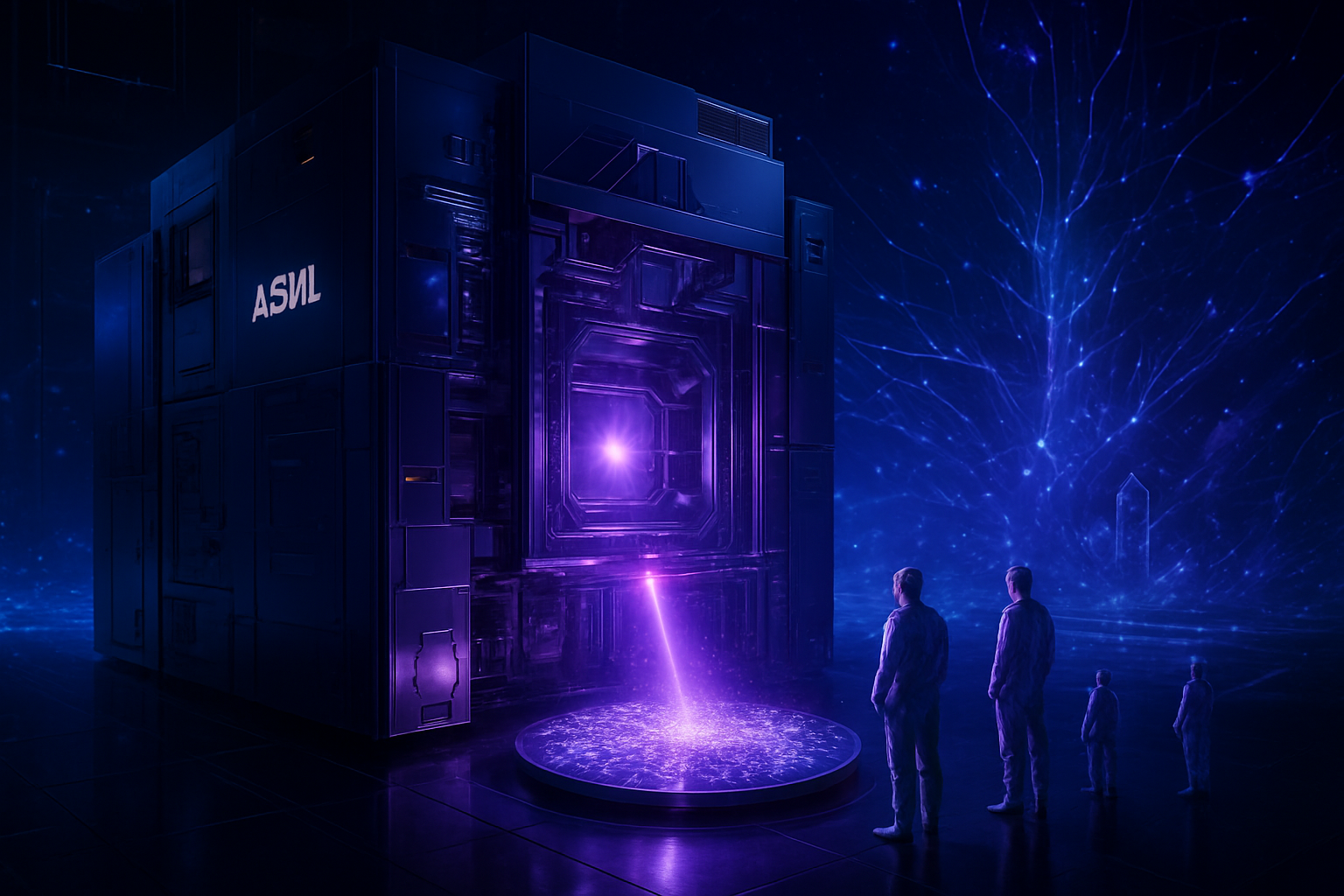
    As of February 2, 2026, the artificial intelligence industry has reached a pivotal milestone with the official finalization and commencement of mass production for the JEDEC HBM4 (JESD270-4) standard. This next-generation High Bandwidth Memory architecture represents more than just a performance boost; it signals a fundamental shift in semiconductor design, effectively bridging the gap between raw storage and processing power. With the first wave of HBM4-equipped silicon hitting the market, the technology is poised to provide the essential "oxygen" for the trillion-parameter Large Language Models (LLMs) that define the current era of agentic AI.

    The finalization of HBM4 comes at a critical juncture as leading AI accelerators, such as the newly unveiled NVIDIA (NASDAQ: NVDA) Vera Rubin and AMD (NASDAQ: AMD) Instinct MI400, demand unprecedented data throughput. By doubling the memory interface width and integrating advanced logic directly into the memory stack, HBM4 promises to shatter the "Memory Wall"—the longstanding bottleneck where processor performance outpaces the speed at which data can be retrieved from memory.

    The 2048-bit Revolution: Engineering the Memory-Logic Fusion

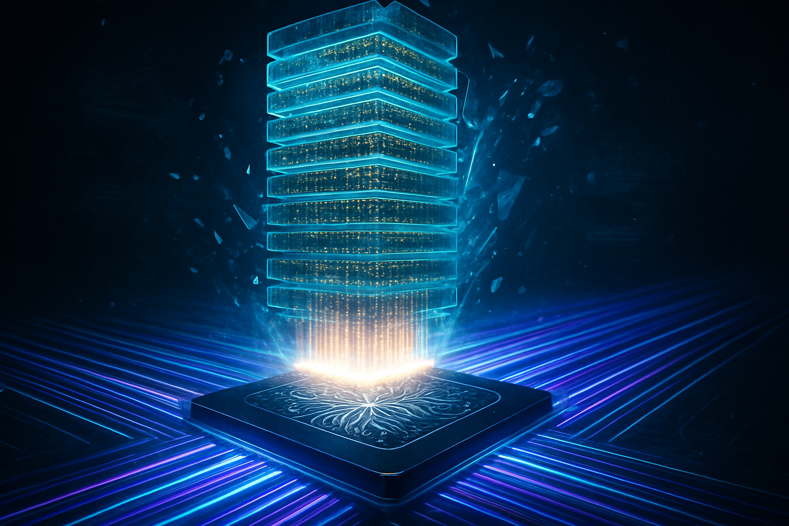
    The technical specifications of HBM4 mark the most radical departure from previous generations since the inception of stacked memory. The most significant change is the doubling of the physical interface from 1024-bit in HBM3E to a massive 2048-bit interface per stack. This wider "data superhighway" allows for aggregate bandwidths exceeding 2.0 TB/s per stack, with advanced implementations reaching up to 3.0 TB/s. To manage this influx of data, JEDEC has increased the number of independent channels from 16 to 32, enabling more granular and parallel access patterns essential for modern transformer-based architectures.

    Perhaps the most revolutionary aspect of the HBM4 standard is the transition of the logic base layer (the bottom die of the stack) to advanced foundry logic nodes. Traditionally, this base layer was manufactured using the same mature DRAM processes as the memory cells themselves. Under the HBM4 standard, manufacturers like Samsung Electronics (KRX: 005930) and SK Hynix (KRX: 000660) are utilizing 4nm and 5nm nodes for this logic die. This shift allows the base layer to be "fused" with the GPU or CPU more effectively, potentially integrating custom controllers or even basic compute functions directly into the memory stack.

    Initial reactions from the research community have been overwhelmingly positive. Dr. Elena Kostic, a senior analyst at SemiInsights, noted that the JEDEC decision to relax the package thickness to 775 micrometers (μm) was a "masterstroke" for the industry. This adjustment allows for 12-high and 16-high stacks—offering capacities up to 64GB per stack—to be manufactured without the immediate, prohibitively expensive requirement for hybrid bonding, though that technology remains the roadmap for the inevitable HBM4E transition.

    The Competitive Landscape: A High-Stakes Race for Dominance

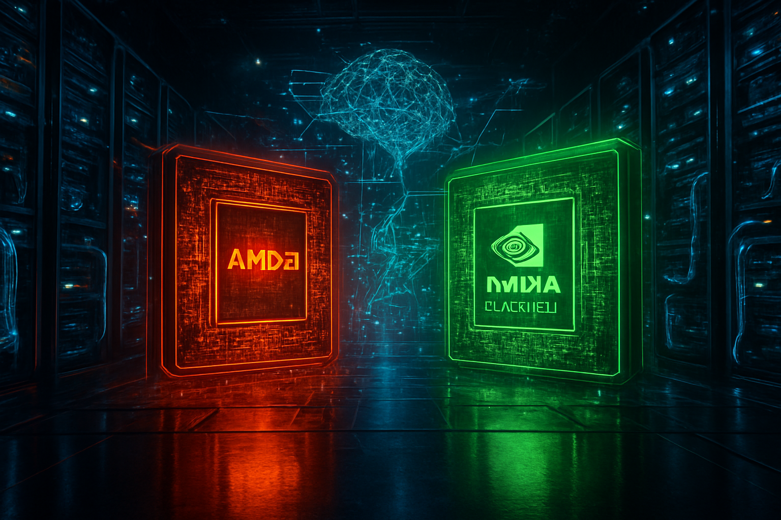
    The finalization of HBM4 has ignited an intense rivalry between the "Big Three" memory makers. SK Hynix, which held a commanding 55% market share at the end of 2025, continues its deep strategic alliance with Taiwan Semiconductor Manufacturing Company (NYSE: TSM) to produce its logic dies. By leveraging TSMC's advanced CoWoS-L (Chip-on-Wafer-on-Substrate) packaging, SK Hynix remains the primary supplier for NVIDIA’s high-end Rubin units, securing its position as the incumbent volume leader.

    However, Samsung Electronics has utilized the HBM4 transition to reclaim technological ground. By leveraging its internal 4nm foundry for the logic base layer, Samsung offers a vertically integrated "one-stop shop" solution. This integration has yielded a reported 40% improvement in energy efficiency compared to standard HBM3E, a critical factor for hyperscalers like Google and Meta (NASDAQ: META) who are struggling with data center power constraints. Meanwhile, Micron Technology (NASDAQ: MU) has positioned itself as the high-efficiency alternative, with its HBM4 production capacity already sold out through the remainder of 2026.

    This development also levels the playing field for AMD. The Instinct MI400 series, built on the CDNA 5 architecture, utilizes HBM4 to offer a staggering 432GB of VRAM per GPU. This massive capacity allows AMD to target the "Sovereign AI" market, providing nations and private enterprises with the hardware necessary to host and train massive models locally without the latency overhead of multi-node clusters.

    Breaking the Memory Wall: Implications for LLM Training and Sustainability

    The wider significance of HBM4 lies in its impact on the economics and sustainability of AI development. For LLM training, memory bandwidth and power consumption are the two most significant operational costs. HBM4’s move to advanced logic nodes significantly reduces the "energy-per-bit" cost of moving data. In a typical training cluster, the HBM4 architecture can reduce total system power consumption by an estimated 20-30% while simultaneously tripling the training speed for models with over 2 trillion parameters.

    This breakthrough addresses the "Memory Wall" that threatened to stall AI progress in late 2025. By allowing more data to reside closer to the processing cores and increasing the speed at which that data can be accessed, HBM4 enables "Agentic AI"—systems capable of complex, multi-step reasoning—to operate in real-time. Without the 22 TB/s aggregate bandwidth now possible in systems like the NVL72 Rubin racks, the latency required for truly autonomous AI agents would have remained out of reach for the mass market.

    Furthermore, the customization of the logic die opens the door for Processing-In-Memory (PIM). This allows the memory stack to handle basic arithmetic and data movement tasks internally, sparing the GPU from mundane operations and further optimizing energy use. As global energy grids face increasing pressure from AI expansion, the efficiency gains provided by HBM4 are not just a technical luxury but a regulatory necessity.

    The Horizon: From HBM4 to Memory-Centric Computing

    Looking ahead, the near-term focus will shift to the transition from 12-high to 16-high stacks. While 12-high is the current production standard, 16-high stacks are expected to become the dominant configuration by late 2026 as manufacturers refine their thinning processes—shaving DRAM wafers down to a mere 30μm. This will likely necessitate the broader adoption of Hybrid Bonding, which eliminates traditional solder bumps to allow for even tighter vertical integration and better thermal dissipation.

    Experts predict that HBM4 will eventually lead to the total "disaggregation" of the data center. Future applications may see HBM4 stacks used as high-speed "memory pools" shared across multiple compute nodes via high-speed interconnects like UALink. This would allow for even more flexible scaling of AI workloads, where memory can be allocated dynamically to different tasks based on their specific needs. Challenges remain, particularly regarding the yield rates of these ultra-thin 16-high stacks and the continued supply constraints of advanced packaging capacity at TSMC.

    A New Era for AI Infrastructure

    The finalization of the JEDEC HBM4 standard marks a definitive turning point in the history of AI hardware. It represents the moment when memory ceased to be a passive storage component and became an active, logic-integrated partner in the compute process. The fusion of the logic base layer with advanced foundry nodes has provided a blueprint for the next decade of semiconductor evolution.

    As mass production ramps up throughout 2026, the industry's focus will move from architectural design to supply chain execution. The winners of this new era will be the companies that can not only design the fastest HBM4 stacks but also yield them at a scale that satisfies the insatiable hunger of the global AI economy. For now, the "Memory Wall" has been dismantled, paving the way for the next generation of super-intelligence.


    This content is intended for informational purposes only and represents analysis of current AI developments.

    TokenRing AI delivers enterprise-grade solutions for multi-agent AI workflow orchestration, AI-powered development tools, and seamless remote collaboration platforms.
    For more information, visit https://www.tokenring.ai/.

  • ASML and the High-NA EUV Monopoly: The Path to 1.4nm

    ASML and the High-NA EUV Monopoly: The Path to 1.4nm

    In a move that solidifies the next decade of semiconductor advancement, ASML (NASDAQ:ASML) has officially moved its High-NA (Numerical Aperture) EUV lithography systems from experimental pilots to commercial production. As of February 2, 2026, the Dutch lithography giant remains the world’s sole provider of these $400 million machines, a monopoly that effectively makes ASML the gatekeeper of the "Angstrom Era." This transition marks a pivotal moment for the industry, as leading-edge foundries race to operationalize the 1.4nm process node—a threshold essential for the next generation of generative AI and high-performance computing.

    The immediate significance of this development cannot be overstated. With the shipment of the latest EXE:5200B systems to key partners, the semiconductor industry has officially entered a high-stakes transition period. While the previous generation of Low-NA EUV machines allowed the industry to reach the 3nm and 2nm milestones, the physical limits of light have necessitated this massive $400 million upgrade to keep Moore’s Law alive. The survival of the global AI roadmap now rests on ASML’s ability to scale production of these massive, complex tools.

    The Technical Leap: Precision at the 8nm Limit

    The technical core of this advancement lies in the increase of the Numerical Aperture from 0.33 in standard EUV machines to 0.55 in High-NA systems. This change allows for a significant improvement in resolution, dropping from approximately 13.5nm to a staggering 8nm. For manufacturers like Intel (NASDAQ:INTC), this enables the printing of ultra-fine transistor features in a single exposure. Previously, reaching these densities required "multi-patterning," a process where a single layer is printed multiple times to achieve the desired resolution—a method that is not only time-consuming but significantly increases the risk of defects and lower yields.

    The new EXE:5200B systems represent a massive leap in throughput as well, capable of processing over 220 wafers per hour. This is a critical specification for high-volume manufacturing (HVM), as it offsets the astronomical cost of the equipment. Furthermore, the integration of High-NA lithography is coinciding with new transistor architectures like RibbonFET 2 (Intel’s second-generation Gate-All-Around) and advanced backside power delivery systems such as PowerDirect. These innovations, when combined with the precision of High-NA EUV, allow for a 15% to 20% improvement in performance-per-watt at the 1.4nm node.

    Initial reactions from the semiconductor research community have been a mix of awe and caution. While experts at organizations like IMEC have lauded the successful realization of 8nm resolution, there is ongoing debate regarding the complexity of the new anamorphic lenses used in these machines. Unlike standard lenses, these optics provide different magnifications in the X and Y directions, requiring chip designers to rethink entire layout strategies. Despite these hurdles, the industry consensus is clear: High-NA is the only viable path to the 1.4nm (Intel 14A) and 1nm (Intel 10A) nodes.

    A Fractured Competitive Landscape

    The adoption of High-NA EUV has created a fascinating strategic divide among the world’s top chipmakers. Intel has taken a definitive first-mover advantage, being the first to receive and operationalize a fleet of High-NA tools at its Oregon D1X facility. CEO Pat Gelsinger’s "all-in" strategy is designed to reclaim process leadership from TSMC (NYSE:TSM) by 2026-2027. By mastering High-NA early, Intel aims to offer its 14A process to external foundry customers before its rivals, positioning itself as the premier manufacturer for the most advanced AI accelerators from companies like NVIDIA (NASDAQ:NVDA).

    In contrast, TSMC has adopted a more conservative and cost-conscious approach. The world’s largest foundry is opting to push its existing 0.33 NA machines to their absolute limit, using complex multi-patterning for its initial A14 (1.4nm) node. TSMC’s leadership has publicly argued that High-NA remains too expensive for mass adoption in the immediate term, preferring to wait until the technology matures and costs normalize before integrating it into their high-volume lines for the A14P or A10 nodes. This creates a high-stakes gamble: can TSMC maintain its yield and cost advantages using older tools, or will Intel’s early adoption of High-NA allow it to leapfrog the industry leader in density and performance?

    Meanwhile, Samsung (KRX:005930) is pursuing a hybrid strategy, utilizing its newly acquired High-NA systems for both its SF1.4 logic node and the development of next-generation Vertical Channel Transistor (VCT) DRAM. Samsung’s focus on AI-centric memory—specifically HBM4 and beyond—makes High-NA essential for maintaining its competitive edge in the memory market. This strategic divergence means that for the first time in a decade, the three major players are taking vastly different technological paths to reach the same destination, with ASML profiting from every choice made.

    Moore’s Law in the Age of Artificial Intelligence

    The broader significance of the High-NA era lies in its role as the physical foundation for the AI revolution. As Large Language Models (LLMs) grow in complexity, the demand for chips with higher transistor density and lower power consumption has become insatiable. The 1.4nm node is not just a numerical milestone; it represents the point where hardware can realistically support the trillion-parameter models expected by the end of the decade. Without the resolution provided by High-NA EUV, the energy requirements for training and inferencing these models would quickly become unsustainable for global power grids.

    This development also underscores the extreme consolidation of the semiconductor supply chain. ASML’s €38.8 billion ($42.1B) order backlog represents a geopolitical reality where the entire world’s technological progress is bottlenecked through a single Dutch company. The concentration of such vital technology has already led to intense export controls and international friction. As we move toward 1.4nm, the "lithography gap" between those who have access to High-NA tools and those who do not will define the next era of economic and military power.

    Comparatively, the shift to High-NA is being viewed as a milestone even more significant than the original transition from DUV (Deep Ultraviolet) to EUV in 2019. While that transition took nearly a decade of delays and false starts, the High-NA rollout has been remarkably precise, driven by the intense pressure of the AI "super-cycle." The success of this transition suggests that Moore's Law—frequently pronounced dead by skeptics—has found a new lease on life through sheer engineering willpower and massive capital investment.

    The Horizon: From 1.4nm to the 1nm Threshold

    Looking ahead, the next 24 to 36 months will be focused on the ramp-up to risk production for the 1.4nm node, expected in 2027. Near-term challenges remain, particularly regarding the development of new photoresists and mask-making materials that can keep up with the 8nm resolution of High-NA systems. Furthermore, the massive power consumption of these machines—each requiring its own dedicated electrical substation—will push semiconductor fabs to invest heavily in sustainable energy infrastructure.

    Beyond 1.4nm lies the elusive 1nm (10 Angstrom) barrier. Experts predict that the EXE:5200 series will be the workhorse for this transition, but even higher NA systems or "Hyper-NA" (0.75 NA) are already being discussed in ASML’s R&D labs. Potential applications on the horizon include edge-AI chips so efficient they can run complex reasoning models on a smartphone battery for days, and specialized processors for quantum-classical hybrid systems. The primary hurdle will not just be physics, but economics: as tools approach the half-billion-dollar mark, only the largest sovereign-backed foundries may be able to afford to stay in the race.

    Summary of the Angstrom Era

    The successful commercialization of High-NA EUV by ASML marks a definitive end to the "nanometer" era and the beginning of the "Angstrom" era. By doubling down on its monopoly and delivering machines capable of 8nm resolution, ASML has provided a roadmap for Intel, Samsung, and TSMC to reach the 1.4nm node and beyond. Intel’s aggressive first-mover strategy stands in stark contrast to TSMC’s cautious optimization, setting the stage for a dramatic shift in market dynamics as we approach 2027.

    The long-term impact of this development will be felt in every sector touched by AI, from autonomous systems to drug discovery. The ability to pack more intelligence into every square millimeter of silicon is the primary engine of modern progress. In the coming months, the industry will be watching for the first yield reports from Intel’s 14A pilot lines and ASML’s ability to meet its ambitious delivery schedule. One thing is certain: the path to 1.4nm is now open, but the cost of entry has never been higher.


    This content is intended for informational purposes only and represents analysis of current AI developments.

    TokenRing AI delivers enterprise-grade solutions for multi-agent AI workflow orchestration, AI-powered development tools, and seamless remote collaboration platforms.
    For more information, visit https://www.tokenring.ai/.

  • Samsung Taylor Fab Commences Risk Production for 2nm Chips

    Samsung Taylor Fab Commences Risk Production for 2nm Chips

    In a move that signals a seismic shift in the global semiconductor landscape, Samsung Electronics (KRX: 005930) has officially commenced risk production for its 2nm (SF2) process node at its $44 billion facility in Taylor, Texas. This milestone marks the first time that cutting-edge 2nm-class silicon has been manufactured on U.S. soil, representing a critical victory for Samsung in its bid to challenge the dominance of Taiwan Semiconductor Manufacturing Company (TPE: 2330).

    The Taylor facility, which has transitioned from its original 4nm mandate to a "2nm-first" strategy, is now operating its first batch of advanced lithography systems. This development is not merely a technical achievement; it is a foundational pillar of the U.S. strategy to secure domestic leading-edge chip production. Supported by $6.4 billion in subsidies from the CHIPS and Science Act, Samsung’s Texas operations are now the epicenter of a "Turnkey" manufacturing ecosystem designed to provide the world’s most advanced AI hardware under one roof.

    Technical Prowess: Third-Generation GAA and CNT Pellicles

    The 2nm process, designated as SF2 by Samsung Foundry, utilizes the third generation of the company’s proprietary Gate-All-Around (GAA) architecture, branded as Multi-Bridge Channel FET (MBCFET). While competitors like TSMC are just beginning their transition to GAA at the 2nm level, Samsung is leveraging nearly four years of telemetry data from its early 3nm GAA production. The SF2 node delivers a 12% increase in performance and a 25% reduction in power consumption compared to the previous 3nm generation. This efficiency is critical for the next wave of hyperscale AI accelerators and mobile processors that are pushing the limits of thermal management.

    A key differentiator in the Taylor fab’s 2nm line is the large-scale implementation of advanced Extreme Ultraviolet (EUV) pellicles. Samsung has adopted Carbon Nanotube (CNT) pellicle technology, which boasts a light transmittance rate exceeding 97%. This is a significant upgrade over traditional silicon-based pellicles, which often suffer from lower transparency and thermal degradation under the high-power EUV beams required for 2nm patterning. By reducing "stochastic" defects and increasing wafer throughput, these CNT pellicles are expected to help Samsung achieve a target yield of 60-70%—a figure that would make it highly competitive with TSMC’s N2 node.

    Furthermore, Samsung is preparing its SF2P (Performance) variant for high-end data center applications, which features specialized channel strain engineering to reduce parasitic capacitance. Initial reactions from the industry have been cautiously optimistic; while Samsung struggled with early 3nm yields, the stabilization of its 2nm process in Taylor suggests that the company has finally overcome the learning curve associated with GAA structures.

    Market Dynamics: Courting AMD, Qualcomm, and Tesla

    Samsung’s strategic pivot to the United States is already paying dividends in terms of customer acquisition. Advanced Micro Devices (NASDAQ: AMD) and Qualcomm (NASDAQ: QCOM) are reportedly in deep negotiations to secure 2nm capacity at the Taylor fab. For Qualcomm, the attraction lies in Samsung’s ability to offer a "dual-sourcing" alternative to TSMC, where Apple has reportedly reserved the lion's share of initial 2nm capacity. Industry insiders suggest that Samsung’s 2nm wafers could be priced as much as 33% lower than TSMC’s, providing a vital margin cushion for chip designers facing rising manufacturing costs.

    The Taylor fab has also secured a cornerstone client in Tesla (NASDAQ: TSLA). The electric vehicle giant is expected to use the facility for its next-generation AI6 autonomous driving chips. By fabbing these chips in Texas, Tesla gains a localized supply chain that minimizes geopolitical risk and logistical overhead. This "Made in USA" advantage is becoming a primary selling point as tech giants look to diversify their manufacturing footprint away from East Asia.

    The competitive landscape is further complicated by Intel (NASDAQ: INTC), which has recently ramped up its 18A node. While Intel currently holds a lead in backside power delivery technology, Samsung’s "Turnkey Strategy"—which integrates 2nm logic, HBM4 memory, and advanced 3D packaging (SAINT)—offers a comprehensive solution that Intel and TSMC struggle to match individually. This holistic approach is particularly attractive to AI startups and hyperscalers that require high-bandwidth memory to be stacked directly onto 2nm logic dies.

    Geopolitics and the AI Hardware Explosion

    The commencement of 2nm risk production in Taylor is a landmark moment in the broader AI landscape. As the demand for NVIDIA (NASDAQ: NVDA) GPUs and custom AI ASICs continues to outpace supply, the addition of a major 2nm hub in the United States provides a necessary safety valve for the industry. It aligns perfectly with the current trend toward sovereign AI, where nations and corporations seek to control their hardware destiny.

    This development also underscores the success of the CHIPS Act in incentivizing leading-edge manufacturing within the U.S. The Taylor campus, now a $44 billion investment, represents one of the largest foreign direct investments in U.S. history. By fostering a "K-Semiconductor Cluster" in Central Texas—including specialized suppliers for EUV pellicles and materials—Samsung is building an ecosystem that will likely influence semiconductor trends for the next decade.

    However, concerns remain regarding the speed of the yield ramp. While 60% yield is a strong start for 2nm, the industry standard for high-volume profitability typically requires upwards of 70-80%. Comparisons to previous milestones, such as the move from 7nm to 5nm, show that the transition to 2nm is orders of magnitude more complex due to the extreme precision required in lithography and the fragility of nanosheet structures.

    The Horizon: From Risk Production to 1.4nm

    Looking ahead, Samsung plans to transition from risk production to full-scale mass production at the Taylor fab by the second half of 2026. This timeline puts them in a neck-and-neck race with TSMC’s Arizona facility. In the near term, we can expect to see the first 2nm-powered consumer devices, likely headlined by Samsung's own Galaxy S27 series and potentially a refreshed line of AI-capable laptops from various OEMs.

    Beyond 2nm, Samsung has already laid out a roadmap for its 1.4nm (SF1.4) node, which is slated for development by late 2027. The Taylor fab is designed to be future-proof, with the infrastructure already in place to support the move to "High-NA" EUV systems from ASML (NASDAQ: ASML) as they become commercially viable. The primary challenge moving forward will be the integration of Backside Power Delivery (BSPDN) in the SF2Z variant, which experts predict will be the next major battleground in semiconductor architecture.

    A Final Assessment of the Taylor Milestone

    The commencement of 2nm risk production at Samsung’s Taylor fab is a definitive "coming of age" moment for the U.S. semiconductor industry and a bold statement of intent from Samsung. By combining its 3rd-generation GAA technology with a multi-billion dollar commitment to American manufacturing, Samsung is not just building a factory; it is attempting to rewrite the rules of the foundry market.

    The significance of this development in AI history cannot be overstated. As AI models become more complex, the hardware that powers them must become more efficient and accessible. The Taylor facility provides the capacity and the cutting-edge tech to meet that demand. In the coming weeks and months, the industry will be watching Samsung’s yield reports and customer announcements closely. If the company can maintain its current momentum, the "Silicon Hills" of Texas may soon become the most important real estate in the global AI economy.


    This content is intended for informational purposes only and represents analysis of current AI developments.

    TokenRing AI delivers enterprise-grade solutions for multi-agent AI workflow orchestration, AI-powered development tools, and seamless remote collaboration platforms.
    For more information, visit https://www.tokenring.ai/.

  • NVIDIA Unveils “Vera Rubin” Platform at CES 2026: A New Era for Agentic AI

    NVIDIA Unveils “Vera Rubin” Platform at CES 2026: A New Era for Agentic AI

    The landscape of artificial intelligence underwent a tectonic shift at CES 2026 as NVIDIA (NASDAQ: NVDA) officially debuted its next-generation "Vera Rubin" platform. Moving beyond the text-generation capabilities of the previous Blackwell era, the Rubin architecture is designed from the ground up to support "Agentic AI"—systems capable of autonomous reasoning, long-term planning, and independent execution of complex workflows. CEO Jensen Huang described the launch as the beginning of the "Reasoning Revolution," where AI transitions from a passive co-pilot to an active, autonomous digital employee.

    The announcement represents more than just a hardware refresh; it is a fundamental redesign of the AI factory. By integrating the new Vera CPU and the R100 GPU with industry-first 6th-gen HBM4 memory, NVIDIA aims to eliminate the "memory wall" that has hindered the development of truly autonomous agents. As global enterprises look to deploy agents that can manage entire supply chains or conduct scientific research with minimal human oversight, the Rubin platform arrives as the essential infrastructure for the next decade of silicon-based intelligence.

    Technical Prowess: The Vera CPU and R100 GPU Deep Dive

    At the heart of the Rubin platform lies a sophisticated "extreme-codesigned" system consisting of the Vera CPU and the R100 GPU. The Vera CPU, succeeding the Grace architecture, features 88 custom "Olympus" cores built on the Arm v9.2 architecture. Utilizing spatial multi-threading, Vera supports 176 concurrent threads, delivering a twofold performance increase over its predecessor. This CPU is specifically tuned to act as the "orchestrator" for agentic tasks, managing the complex logic and tool-use protocols required when an AI agent interacts with external software or hardware.

    The R100 GPU is the platform's powerhouse, manufactured on TSMC’s (NYSE: TSM) advanced 3nm process. It boasts a staggering 336 billion transistors and introduces the 3rd-generation Transformer Engine. Most notably, the R100 features redesigned Streaming Multiprocessors (SMs) optimized for "Tree-of-Thought" processing. This allows the GPU to explore multiple logical paths simultaneously and discard unproductive reasoning branches in real-time, a capability crucial for models like OpenAI’s o1 or Google’s (NASDAQ: GOOGL) latest reasoning-heavy architectures.

    The most significant bottleneck in AI—memory bandwidth—has been addressed through the integration of 6th-generation HBM4 memory. Each R100 GPU is equipped with 288GB of HBM4, providing an aggregate bandwidth of 22 TB/s. This represents a nearly threefold increase over the Blackwell generation. Through NVLink-C2C, the Vera CPU and Rubin GPUs share a unified memory pool, allowing for the seamless data movement necessary to handle trillion-parameter models that require massive "test-time scaling," where the system "thinks" longer to produce more accurate results.

    Reshaping the AI Market: The End of the "Inference Tax"

    The introduction of the Rubin architecture sends a clear signal to the rest of the tech industry: the cost of intelligence is about to plummet. NVIDIA claims the platform reduces the cost per token by 10x while delivering 5x faster inference performance compared to Blackwell. This reduction is critical for cloud service providers like Amazon (NASDAQ: AMZN) AWS, Microsoft (NASDAQ: MSFT) Azure, and Oracle (NYSE: ORCL), who are all slated to receive the first Rubin-powered systems in the second half of 2026. By lowering the "inference tax," NVIDIA is making it economically viable for startups to deploy persistent, always-on AI agents that were previously too expensive to maintain.

    For competitors like AMD (NASDAQ: AMD) and Intel (NASDAQ: INTC), the Rubin platform raises the bar for what constitutes an "AI chip." NVIDIA is no longer just selling silicon; it is selling a rack-scale computer—the NVL72—which acts as a single, massive GPU. The inclusion of the BlueField-4 DPU for context memory management and Spectrum-X silicon photonics networking ensures that NVIDIA maintains its "moat" by providing a vertically integrated stack that is difficult for rivals to replicate piece-meal.

    A Wider Significance: From Pattern Matching to Autonomous Reasoning

    The Vera Rubin platform marks the transition of the industry from the "Generative Era" to the "Reasoning Era." For the past three years, AI has been largely characterized by high-speed pattern matching. The Rubin architecture is the first hardware platform specifically built for "Closed-Loop Science" and autonomous reasoning. During the CES demonstration, NVIDIA showcased agents hypothesized new chemical compounds, simulated their properties, and then directed robotic lab equipment to synthesize them—all running locally on a Rubin cluster.

    This shift has profound implications for the broader AI landscape. By enabling "test-time scaling," Rubin allows AI models to spend more compute cycles on reasoning rather than just outputting the next likely word. This addresses a major concern in the research community: the plateauing of model performance based on data scaling alone. If models can "think" their way through problems using Rubin’s specialized SMs, the path to Artificial General Intelligence (AGI) may no longer depend solely on scraping more internet data, but on more efficient, autonomous logical exploration.

    The Horizon: Future Developments and Agentic Workflows

    Looking ahead, the rollout of the Rubin platform in late 2026 is expected to trigger a wave of "Agentic Workflows" across various sectors. In the near term, we expect to see the rise of "Digital Employees" in software engineering, legal discovery, and financial modeling—agents that can work for hours or days on a single prompt. The long-term challenge will be the massive power requirements of these reasoning-heavy tasks. While Rubin is more efficient per-token, the sheer volume of autonomous agents could strain global energy grids, prompting further innovation in liquid cooling and sustainable data center design.

    Experts predict that the next phase of development will focus on "Inter-Agent Collaboration." With the Rubin platform's high-speed NVLink 6 interconnect, thousands of specialized agents could potentially work together in a single rack, functioning like a synthetic department within a company. The primary hurdle will be creating the software frameworks to manage these fleets of agents, a task NVIDIA hopes to solve with its expanded CUDA-X libraries and NIM microservices.

    Conclusion: A Landmark in AI History

    NVIDIA’s unveiling of the Vera Rubin platform at CES 2026 is a defining moment in the history of computing. By providing the specialized hardware necessary for autonomous reasoning and agentic behavior, NVIDIA has effectively set the stage for the next phase of the digital revolution. The combination of Vera CPUs, R100 GPUs, and HBM4 memory breaks the traditional barriers of memory and logic that have constrained AI until now.

    As the industry prepares for the delivery of these systems in H2 2026, the focus will shift from what AI can say to what AI can do. The Rubin architecture isn't just a faster processor; it is the foundation for a world where autonomous digital entities become an integral part of the workforce. For investors, developers, and society at large, the message from CES 2026 is clear: the era of the reasoning agent has officially arrived.


    This content is intended for informational purposes only and represents analysis of current AI developments.

    TokenRing AI delivers enterprise-grade solutions for multi-agent AI workflow orchestration, AI-powered development tools, and seamless remote collaboration platforms.
    For more information, visit https://www.tokenring.ai/.

  • US-Taiwan Trade Deal: Lower Tariffs to Fuel Arizona “Gigafab” Cluster

    US-Taiwan Trade Deal: Lower Tariffs to Fuel Arizona “Gigafab” Cluster

    On January 15, 2026, the United States and Taiwan finalized a landmark economic agreement, colloquially known as the "Silicon Pact," which drastically reduces trade barriers for semiconductor components and materials. This strategic trade deal is set to accelerate the development of the "Gigafab" cluster in Phoenix, Arizona, a massive industrial hub centered around Taiwan Semiconductor Manufacturing Company (TSMC) (NYSE: TSM). By slashing reciprocal tariffs to 15% and providing unique "national security" duty exemptions, the deal removes the final economic hurdles for a fully domestic, advanced AI hardware supply chain.

    The immediate significance of this agreement cannot be overstated. As of February 2, 2026, the Arizona cluster has transitioned from a localized manufacturing site into a self-sufficient "megacity of silicon." With the trade deal now in effect, the cost of importing specialized chemicals, high-precision tooling, and raw wafers from Taiwan has plummeted. This fiscal relief is incentivizing a second wave of Taiwanese suppliers to relocate to the Sonoran Desert, ensuring that the critical chips powering the next generation of artificial intelligence are not just designed in America, but entirely fabricated and packaged on U.S. soil.

    The Silicon Pact: Technical Specifications and the Roadmap to 2nm

    The 2026 trade agreement introduces a sophisticated "reward for investment" mechanism. Specifically, Taiwanese companies expanding their U.S. capacity are granted exemptions from Section 232 duties, which previously added significant costs to steel, aluminum, and related derivative products used in fab construction. Under the new rules, companies like TSMC can import up to 2.5 times their planned U.S. capacity of wafers and chips duty-free during construction phases. Once operational, they retain a perpetual allowance to import 1.5 times their production capacity, creating a flexible hybrid supply chain that bridges the Pacific.

    Technically, the Arizona Gigafab cluster is reaching unprecedented milestones. Fab 1 is currently in high-volume manufacturing (HVM) for 4nm and 5nm nodes, achieving yield rates of 88–92%—parity with TSMC’s flagship facilities in Hsinchu. Meanwhile, Fab 2 is entering the equipment installation phase for 3nm production, with a target start date in early 2027. Most ambitiously, foundation work for Fab 3 is now complete; this facility is designed to produce 2nm and A16 (1.6nm) chips featuring Gate-All-Around (GAA) transistor architecture. This roadmap ensures that by 2030, roughly 30% of TSMC’s global 2nm capacity will be located within the Arizona cluster.

    This development differs from previous onshoring efforts by focusing on the entire ecosystem rather than just the fab itself. The trade deal specifically rewards the "clustering" of suppliers. Companies such as Chang Chun Group, Sunlit Chemical, and LCY Chemical have already opened facilities in Arizona to provide ultra-pure hydrogen peroxide and electronic-grade isopropyl alcohol. The arrival of ASML (NASDAQ: ASML) with a massive 56,000-square-foot training center in Phoenix further cements the region as a global hub for lithography expertise, marking a shift from a "satellite fab" model to a complete, vertically integrated industrial cluster.

    Market Implications for AI Giants and Startups

    The primary beneficiaries of the Arizona Gigafab cluster are the titans of the AI industry. Nvidia (NASDAQ: NVDA) has already designated the Arizona site as a primary production hub for its Blackwell-series GPUs, which are the backbone of modern large language models. Similarly, Apple (NASDAQ: AAPL) continues to utilize the cluster for its A-series and M-series chips, which now feature advanced Neural Engines for on-device generative AI. For these companies, the trade deal provides a "Made in USA" certification that is increasingly vital for government contracts and domestic security requirements.

    Beyond the established giants, the cluster is attracting major investment from hyperscalers like Microsoft (NASDAQ: MSFT). Microsoft is reportedly sourcing its Maia 200 AI inference accelerators—built on the 3nm node—through the TSMC ecosystem and is prioritizing its Arizona-based data centers to reduce latency and logistical overhead. Even OpenAI, working through partnerships with Broadcom (NASDAQ: AVGO), is expected to leverage the Arizona cluster for its future custom-designed training and inference silicon. This shift represents a massive disruption to the traditional "hub-and-spoke" model, where silicon had to travel thousands of miles for packaging before returning to the U.S.

    The strategic advantage for these companies lies in supply chain resilience. By capping duties and stabilizing the cost of materials, the Silicon Pact removes the volatility associated with geopolitical tensions in the Taiwan Strait. For startups and smaller AI labs, the emergence of a domestic cluster means more predictable lead times and potentially lower "cost-per-token" for AI inference as the domestic supply of high-end chips increases. The competition is now moving from who can design the best chip to who can secure the most capacity in the Arizona cluster.

    Geopolitical Security and the Broader AI Landscape

    The US-Taiwan trade deal is a cornerstone of a broader trend toward "techno-nationalism" and supply chain diversification. In the wider AI landscape, the Arizona cluster serves as a hedge against the single-point-of-failure risk that has loomed over the industry for a decade. By de-risking the manufacturing process, the U.S. and Taiwan are creating a "silicon shield" that is economic rather than purely military. This fits into the ongoing global trend of regionalizing high-tech manufacturing, similar to the EU’s efforts with its own Chips Act.

    However, the rapid expansion of the Arizona cluster is not without concerns. The environmental impact on the arid Sonoran Desert is a frequent point of discussion. To address this, the 2026 agreement includes provisions for "green manufacturing" infrastructure, funding massive water recycling plants that allow fabs to reuse up to 98% of their industrial water. Furthermore, there are ongoing labor challenges, as the demand for highly specialized semiconductor engineers in Phoenix currently outstrips local supply, necessitating the ASML training centers and university partnerships funded by the trade deal.

    Comparatively, this milestone is as significant as the original founding of TSMC in the 1980s. It represents the first time that the world’s most advanced lithography (3nm and below) has been successfully transplanted to a different continent at scale. The geopolitical significance of having NVIDIA Blackwell GPUs and future 2nm "superchips" manufactured in a domestic "Gigafab" cluster provides the U.S. with a level of technological sovereignty that seemed impossible only five years ago.

    The Road Ahead: Packaging and 1.6nm Nodes

    Looking toward the near-term, the next major development will be the integration of advanced packaging. Historically, even chips made in the U.S. had to be sent back to Taiwan for CoWoS (Chip-on-Wafer-on-Substrate) packaging. By late 2026, TSMC and Amkor Technology (NASDAQ: AMKR) are expected to finalize their domestic advanced packaging facilities in Arizona. This will create a "turnkey" solution where raw silicon enters the Phoenix site and emerges as a fully packaged, ready-to-deploy AI accelerator.

    In the long term, the industry is watching the 1.6nm (A16) node. Experts predict that the Arizona cluster will be the first site outside of Taiwan to implement A16 technology, which is essential for the 1,000W+ superchips required for "General Purpose AI" (GPAI). The challenge will be maintaining the high yields as the technology moves toward the atomic limit. If TSMC can successfully transition its Arizona cluster to GAA transistors at 2nm and beyond, it will solidify the region as the premier semiconductor hub of the 21st century.

    A New Era for American Silicon

    The finalization of the US-Taiwan "Silicon Pact" in early 2026 marks the beginning of a new era for American manufacturing and global AI development. By reducing tariffs and incentivizing a dense cluster of suppliers, the trade deal has transformed Arizona into a global epicenter for advanced semiconductor fabrication. The key takeaways are clear: the AI hardware supply chain is no longer a fragile, trans-Pacific line, but a robust, domestic ecosystem capable of supporting the world's most demanding computational needs.

    As we move through the remainder of 2026, the industry should watch for the first "Arizona-packaged" Blackwell GPUs and the progress of tool installation in Fab 2. This development's significance in AI history will likely be viewed as the moment the physical "foundations" of the AI revolution were finally secured. The long-term impact will be felt in every sector of the economy, from autonomous vehicles to personalized medicine, all powered by the silicon emerging from the Arizona desert.


    This content is intended for informational purposes only and represents analysis of current AI developments.

    TokenRing AI delivers enterprise-grade solutions for multi-agent AI workflow orchestration, AI-powered development tools, and seamless remote collaboration platforms.
    For more information, visit https://www.tokenring.ai/.

  • The $1 Trillion Milestone: Semiconductor Revenue to Peak in 2026

    The $1 Trillion Milestone: Semiconductor Revenue to Peak in 2026

    As of February 2, 2026, the global semiconductor industry has reached a historic inflection point. New data from major industry analysts confirms that annual revenue is on track to hit the $1 trillion mark by the end of 2026, a milestone that was previously not expected until 2030. This unprecedented acceleration is being driven by the "AI Hardware Super-cycle," a period of intense capital expenditure as nations and corporations race to build out the physical infrastructure required for agentic and physical artificial intelligence.

    The achievement marks a transformative era for the global economy, where silicon has officially replaced oil as the world’s most critical commodity. With total revenue hitting approximately $793 billion in 2025, the projected 26.3% growth for 2026—led by record-breaking demand for high-performance logic and memory—is set to push the industry past the trillion-dollar threshold. This surge reflects more than just a temporary spike; it represents a structural shift in how compute power is valued, consumed, and manufactured.

    Technical Drivers: HBM4 and the 2nm Transition

    The technical backbone of this $1 trillion milestone is the simultaneous transition to next-generation memory and logic architectures. In 2026, the industry has seen the rapid adoption of HBM4 (High Bandwidth Memory 4), which provides the staggering 3.6 TB/s+ bandwidth required by NVIDIA (NASDAQ: NVDA) and their new "Rubin" GPU architecture. This high-performance memory is no longer a niche component; it has become the primary bottleneck for AI performance, leading manufacturers like SK Hynix and Samsung to reallocate massive portions of their DRAM production capacity away from consumer electronics toward AI data centers.

    Simultaneously, the move to 2-nanometer (2nm) logic nodes has given foundries unprecedented pricing power. TSMC (NYSE: TSM) remains the dominant player in this space, with its 2nm capacity reportedly fully booked through 2027 by a handful of "hyperscalers" and chip designers. These advanced nodes offer a 15% performance boost and a 30% reduction in power consumption compared to the 3nm process, making them essential for the energy-efficient operation of massive AI clusters. Furthermore, the rise of domain-specific ASICs (Application-Specific Integrated Circuits) from companies like Broadcom (NASDAQ: AVGO) and Marvell (NASDAQ: MRVL) has introduced a new layer of high-margin silicon designed specifically for internal workloads at Google and Meta.

    The Corporate Winner's Circle: A New Industry Hierarchy

    This revenue peak has fundamentally reshaped the competitive landscape of the technology sector. NVIDIA has solidified its position as the world's most valuable semiconductor company, becoming the first in history to cross $125 billion in annual revenue. Their dominance in the data center market has created a "toll booth" effect, where almost every major AI breakthrough relies on their Blackwell or Rubin platforms. Meanwhile, TSMC continues to act as the industry's indispensable foundry, with its revenue expected to grow by over 30% in 2026 as it scales 2nm production.

    The shift has also produced surprising upsets in the traditional hierarchy. Driven by its mastery of the HBM supply chain, SK Hynix has officially overtaken Intel (NASDAQ: INTC) in quarterly revenue as of late 2025, securing its spot as the third-largest semiconductor firm globally. While Intel and AMD (NASDAQ: AMD) continue to battle for the "AI PC" and server CPU markets, the real profit margins have migrated toward the specialized accelerators and high-speed networking components provided by companies like ASML (NASDAQ: ASML), whose High-NA EUV lithography machines are now the gatekeepers of sub-2nm manufacturing.

    Comparing Cycles: Why the AI Super-Cycle is Different

    To understand the magnitude of the $1 trillion milestone, analysts are comparing the current growth to previous industry cycles. The 2000s were defined by the PC and the early internet build-out, while the 2010s were fueled by the smartphone and cloud computing revolution. However, the 2020s "AI Super-cycle" is distinct in its concentration and intensity. Unlike the "tide lifts all ships" era of the 2010s, the current market is highly bifurcated. While AI and automotive silicon (driven by advanced driver-assistance systems) are seeing explosive growth, traditional sectors like low-end consumer electronics are facing "inventory drag" and rising costs as resources are diverted to AI production.

    Furthermore, the concept of "Sovereign AI" has added a geopolitical layer to the market that did not exist during the mobile revolution. Governments in the US, EU, and Asia are now treating semiconductor capacity as a matter of national security, leading to massive subsidies and the localization of supply chains. This "regionalization" of the industry has created a floor for demand that is largely independent of consumer spending cycles, as nations race to ensure they have the domestic compute power necessary to run their own governmental and military AI models.

    Future Horizons: Beyond the Trillion-Dollar Mark

    Looking ahead, experts do not expect the momentum to stall at $1 trillion. The near-term focus is shifting toward Silicon Photonics, a technology that uses light instead of electricity to transfer data between chips. This transition is viewed as the only way to overcome the physical interconnect limits of traditional copper wiring as AI models continue to grow in size. Analysts predict that by 2028, silicon photonics will be a standard feature in high-end AI clusters, driving the next wave of infrastructure upgrades.

    On the horizon, the transition to 1.4nm nodes (the "Angstrom era") and the rise of "Physical AI"—robotics and autonomous systems that require edge-compute capabilities—are expected to drive the market toward $1.5 trillion by the end of the decade. The primary challenge remains the energy crisis; as chip revenue grows, so does the power consumption of the data centers that house them. Addressing the sustainability of the "Trillion-Dollar Silicon Era" will be the defining technical hurdle of the late 2020s.

    The Silicon Century: A Comprehensive Wrap-Up

    The crossing of the $1 trillion revenue threshold in 2026 marks the official commencement of the "Silicon Century." Semiconductors are no longer just components within gadgets; they are the foundational layer of modern civilization, powering everything from global logistics to scientific discovery. The AI hardware super-cycle has compressed a decade's worth of growth into just a few years, rewarding those companies—like NVIDIA, TSMC, and SK Hynix—that moved most aggressively to capture the high-performance compute market.

    As we move into the middle of 2026, the industry's significance will only continue to grow. Investors and policymakers should watch for the deployment of the first 2nm-powered consumer devices and the potential for a "second wave" of growth as agentic AI begins to permeate the enterprise sector. While the road to $1 trillion was paved by hardware, the long-term impact will be felt in the software and services that this massive infrastructure will soon enable.


    This content is intended for informational purposes only and represents analysis of current AI developments.

    TokenRing AI delivers enterprise-grade solutions for multi-agent AI workflow orchestration, AI-powered development tools, and seamless remote collaboration platforms.
    For more information, visit https://www.tokenring.ai/.

  • Intel 18A Node Reaches High-Volume Production in Arizona

    Intel 18A Node Reaches High-Volume Production in Arizona

    In a move that signals a tectonic shift in the global semiconductor landscape, Intel (NASDAQ: INTC) has officially commenced high-volume manufacturing (HVM) of its pioneering Intel 18A process node at its Ocotillo campus in Chandler, Arizona. This milestone marks the successful completion of CEO Pat Gelsinger’s audacious "5 nodes in 4 years" (5N4Y) roadmap, a strategic sprint designed to reclaim the company's manufacturing leadership after years of falling behind its Asian competitors. The 18A node, roughly equivalent to 1.8nm-class technology, is not just a hardware milestone; it is the foundational platform for the next generation of artificial intelligence, providing the power efficiency and transistor density required for advanced neural processing units (NPUs) and massive data center deployments.

    The immediate significance of this launch lies in Intel’s "first-mover" advantage with two revolutionary technologies: RibbonFET and PowerVia. By beating rivals Taiwan Semiconductor Manufacturing Co. (NYSE: TSM) and Samsung (KRX: 005930) to the implementation of backside power delivery at scale, Intel has positioned itself as the primary alternative for AI chip designers who are increasingly constrained by the thermal and power limits of traditional silicon architectures. As of early 2026, the 18A ramp is already supporting flagship products such as "Panther Lake" for AI PCs and "Clearwater Forest" for high-density server environments, effectively signaling that the "process gap" between Intel and the world's leading foundries has been closed.

    The Technical Frontier: RibbonFET and PowerVia

    The Intel 18A node represents the most significant architectural overhaul of the transistor since the introduction of FinFET in 2011. At the heart of this advancement is RibbonFET, Intel’s proprietary implementation of Gate-All-Around (GAA) technology. Unlike the previous FinFET design, where the gate only covers three sides of the channel, RibbonFET wraps the gate entirely around the silicon channel. This provides significantly better electrical control, reducing current leakage—a critical factor as transistors shrink toward the atomic scale—and allowing for higher drive currents that translate directly into faster switching speeds.

    Equally transformative is PowerVia, Intel’s breakthrough in backside power delivery. Traditionally, power lines and signal wires are woven together on the front side of a chip, leading to "wiring congestion" that slows down performance and generates excess heat. PowerVia separates these functions, moving the entire power delivery network to the back of the silicon wafer. Initial data from the Arizona HVM lines indicates that PowerVia reduces voltage droop by up to 30% and enables a 6% boost in clock frequencies at identical power levels compared to front-side delivery. This "de-cluttering" of the wafer's front side has also enabled Intel to achieve a transistor density of approximately 238 million transistors per square millimeter (MTr/mm²).

    The industry response to these technical specifications has been one of cautious optimism turning into a full-scale endorsement. Early yield reports from the Ocotillo fabs suggest that Intel has achieved a stable yield rate between 55% and 75% for 18A, a threshold that many analysts believed would take much longer to reach. Experts in the AI research community note that the 15% performance-per-watt improvement over the previous Intel 3 node is specifically optimized for "always-on" AI workloads, where efficiency is just as critical as raw throughput.

    Disrupting the Foundry Monopoly

    The successful launch of 18A in Arizona has profound implications for the global foundry market, where TSMC (NYSE: TSM) has long enjoyed a near-monopoly on the most advanced nodes. With 18A now in high-volume production, Intel Foundry is no longer a theoretical competitor but a tangible threat. Tech giants such as Microsoft (NASDAQ: MSFT) and Amazon (NASDAQ: AMZN) have already signed on as major 18A customers, seeking to leverage Intel’s domestic manufacturing footprint to secure their AI supply chains. For Microsoft, the 18A node will likely power future iterations of its custom Maia AI accelerators, reducing its total dependence on external foundries.

    The competitive pressure is now squarely on TSMC and Samsung. While TSMC’s N2 (2nm) node boasts a slightly higher raw transistor density, it lacks backside power delivery, a feature TSMC does not plan to integrate until its A16 node in late 2026 or early 2027. This gives Intel a temporary "feature lead" that is attracting designers of high-performance AI silicon who need the thermal benefits of PowerVia today. Samsung, despite being the first to market with GAA technology at 3nm, has reportedly struggled with yields on its SF2 (2nm) node, leaving an opening for Intel to capture the "Number Two" spot in the global foundry rankings.

    Furthermore, the 18A node’s integration with Intel’s Foveros Direct 3D packaging technology allows for the stacking of compute tiles directly on top of each other with copper-to-copper bonding. This allows startups and AI labs to design modular "chiplet" architectures that combine 18A logic with cheaper, mature nodes for I/O, drastically lowering the barrier to entry for custom AI silicon. By offering both the cutting-edge node and the advanced packaging in a single "systems foundry" approach, Intel is repositioning itself as a one-stop-shop for the AI era.

    A New Era for the AI Landscape

    The arrival of 18A marks a pivotal moment in the broader AI landscape, moving the industry away from "AI software optimization" and back toward "silicon-led innovation." As large language models (LLMs) continue to grow in complexity, the hardware bottleneck has become the primary constraint for AI development. Intel 18A directly addresses this by providing the thermal headroom necessary for more aggressive NPU designs. This development fits into a larger trend of "Sovereign AI," where nations and corporations seek to control their own hardware destiny to ensure security and supply stability.

    The geopolitical significance of the Arizona production cannot be overstated. By achieving HVM of 18A on U.S. soil, Intel is fulfilling a core objective of the CHIPS and Science Act, providing a secure, leading-edge domestic supply of the chips that power critical infrastructure and defense systems. This creates a "silicon shield" for the U.S. tech industry, mitigating the risks associated with the geographic concentration of semiconductor manufacturing in East Asia.

    However, the rapid transition to 1.8nm-class technology also raises concerns regarding the environmental footprint of such advanced manufacturing. The extreme ultraviolet (EUV) lithography required for 18A is immensely energy-intensive. Intel has countered these concerns by committing to 100% renewable energy use at its Ocotillo campus by 2030, but the sheer scale of the 18A ramp-up will be a test for the company’s sustainability goals. Compared to previous milestones like the move to 10nm, the 18A launch is characterized by its focus on "performance-per-watt" rather than just "more transistors," reflecting the energy-hungry reality of modern AI.

    The Road to 14A and Beyond

    Looking ahead, the high-volume production of 18A is merely the beginning of Intel’s long-term roadmap. The company is already looking toward Intel 14A, which will introduce High-NA (Numerical Aperture) EUV lithography to further push the boundaries of miniaturization. Expected to enter risk production in late 2026 or early 2027, 14A will build upon the RibbonFET and PowerVia foundation established by 18A. In the near term, the industry will be watching the market reception of "Panther Lake" CPUs, which will serve as the first major commercial test of 18A’s performance in the hands of consumers.

    Future applications on the horizon include "Edge AI" devices that can run complex generative models locally without needing a cloud connection. The efficiency gains of 18A are expected to enable 24-hour battery life on AI-enhanced laptops and more sophisticated autonomous vehicle controllers that can process sensor data with minimal latency. Challenges remain, particularly in scaling the production of Foveros Direct packaging and managing the complex supply chain for the rare materials required for 1.8nm features, but experts predict that Intel’s successful 5N4Y execution has restored the "tick-tock" rhythm of innovation that the company was once famous for.

    Summary and Final Thoughts

    The start of high-volume production for Intel 18A in Arizona is more than just a company milestone; it is a signal that the era of uncontested dominance by a single foundry is over. By delivering on the "5 nodes in 4 years" promise, Intel has re-established its technical credibility and provided the AI industry with a powerful new toolkit. The combination of RibbonFET and PowerVia offers a glimpse into the future of semiconductor physics, where performance is derived from clever 3D architecture as much as it is from shrinking dimensions.

    As we move further into 2026, the success of 18A will be measured by its ability to win over the "hyperscalers" and maintain its yield advantage over TSMC’s upcoming 2nm offerings. For the first time in a decade, the silicon crown is up for grabs, and Intel has officially entered the ring. Investors and tech enthusiasts should watch for upcoming quarterly reports to see how 18A orders from external foundry customers are scaling, as these will be the ultimate barometer of Intel's long-term resurgence in the AI-driven economy.


    This content is intended for informational purposes only and represents analysis of current AI developments.

    TokenRing AI delivers enterprise-grade solutions for multi-agent AI workflow orchestration, AI-powered development tools, and seamless remote collaboration platforms.
    For more information, visit https://www.tokenring.ai/.

  • Silicon Sovereignty: Assessing the U.S. CHIPS Act’s Path to 20% Global Share by 2030

    Silicon Sovereignty: Assessing the U.S. CHIPS Act’s Path to 20% Global Share by 2030

    As of January 30, 2026, the United States' ambitious effort to repatriate semiconductor manufacturing has officially transitioned from a period of legislative hype and groundbreaking ceremonies to a reality of high-volume manufacturing (HVM). With over $30 billion in federal awards from the CHIPS and Science Act now flowing into the ecosystem, the "Silicon Desert" of Arizona and the "Silicon Prairie" of Texas are no longer just construction sites; they are the front lines of a new era in American industrial policy. The recent commencement of production at key facilities marks a pivotal moment for the Biden-era initiative, signaling that the goal of producing 20% of the world’s leading-edge logic chips by 2030 is not only achievable but potentially conservative.

    The significance of this milestone cannot be overstated for the artificial intelligence sector. By securing domestic production of the sub-2nm nodes required for the next generation of AI accelerators, the U.S. is mitigating the "single point of failure" risk associated with concentrated production in East Asia. As of this month, the first wafers of advanced 1.8nm chips are beginning to move through domestic facilities, providing the hardware foundation for the "Sovereign AI" movement—a strategic push to ensure that the computational power driving the world's most sensitive AI models is born and bred on American soil.

    The Milestone Map: Intel, Micron, and TI Lead the Charge

    The start of 2026 has brought a series of technical triumphs for the program’s heavy hitters. Intel Corporation (NASDAQ:INTC) has officially achieved High-Volume Manufacturing at its Fab 52 in Ocotillo, Arizona. This facility is the first in the world to scale the Intel 18A (1.8nm) process node, which introduces two revolutionary technologies: PowerVia backside power delivery and RibbonFET gate-all-around transistors. This development represents a massive technical leap, allowing for more efficient power routing and higher transistor density than traditional FinFET architectures. While Intel’s massive project in New Albany, Ohio, has seen its timeline shifted to a 2030 production start due to labor and supply chain complexities, the success in Arizona provides the proof of concept that the U.S. can indeed lead in the sub-2nm race.

    Simultaneously, Texas Instruments (NASDAQ:TXN) reached a major milestone in December 2025 with the start of production at its SM1 fab in Sherman, Texas. Unlike Intel’s focus on bleeding-edge logic, TI is bolstering the domestic supply of 300mm analog and embedded processing chips. These "foundational" chips are the unsung heroes of the AI revolution, essential for the power management systems in massive data centers and the edge devices that bring AI to the physical world. With the shell of the second fab, SM2, already completed, TI is ahead of schedule in its $40 billion Texas expansion, reinforcing the resilience of the broader electronics supply chain.

    In the memory sector, Micron Technology (NASDAQ:MU) officially broke ground on its $100 billion megafab in Clay, New York, on January 16, 2026. This project, which followed a rigorous multi-year environmental and regulatory review, is set to become one of the largest semiconductor facilities in history. While the New York site focuses on long-term DRAM capacity, Micron’s Boise, Idaho, expansion (ID2) is moving faster, with equipment installation currently underway to meet a 2027 production target. These facilities are critical for the AI industry, as High-Bandwidth Memory (HBM) remains the primary bottleneck for training increasingly large LLMs (Large Language Models).

    Reshaping the Competitive Landscape for AI Giants

    The transition to domestic production is forcing a strategic pivot for the world's leading AI chip designers. Companies like NVIDIA (NASDAQ:NVDA) and Advanced Micro Devices (NASDAQ:AMD) have long relied on a "fabless" model, outsourcing nearly all high-end production to Taiwan Semiconductor Manufacturing Company (NYSE:TSM). However, a new 25% tariff on imports of advanced computing chips, which went into effect on January 15, 2026, has fundamentally altered the math. To maintain margins and ensure supply security, these giants are now incentivized to utilize the expanding "Sovereign AI" capacity within the U.S.

    The geopolitical and market positioning of these companies is also being influenced by the U.S. government's shift toward a "National Champion" model. In a landmark move, the federal government converted a portion of Intel’s $8.5 billion grant into a 9.9% equity stake, effectively making the Department of Commerce a strategic partner in Intel's success. This ensures that the interests of the U.S. foundry business are closely aligned with national security priorities, such as the Pentagon’s "Secure Enclave" program. For competitors like Samsung Electronics (KRX:005930), which is also ramping up its 2nm capacity in Taylor, Texas, the competition for federal support and domestic contracts has never been fiercer.

    The Global Shift Toward Onshore AI Infrastructure

    The broader significance of these milestones lies in the decoupling of the AI value chain from traditional geopolitical flashpoints. For decades, the tech industry operated under the assumption that globalized supply chains were the most efficient path forward. The CHIPS Act progress in 2026 proves that a state-led industrial policy can successfully counter-balance market forces to re-shore critical infrastructure. Analysts now project that the U.S. will hold approximately 22% of global advanced semiconductor capacity by 2030, exceeding the original 20% target set by the Department of Commerce.

    This shift is not without its controversies and concerns. The imposition of aggressive tariffs and the use of government equity stakes represent a departure from traditional free-market principles, drawing comparisons to the dirigisme models of the mid-20th century. Furthermore, the reliance on a few "mega-projects" creates a high-stakes environment where any delay—such as those seen in Intel’s Ohio project—can have ripple effects across the entire national security apparatus. However, compared to the supply chain chaos of the early 2020s, the current trajectory provides a much-needed sense of stability for the AI research community and enterprise buyers.

    Looking Ahead: The Workforce and the Next Generation

    As the industry moves from pouring concrete to etching silicon, the focus for 2027 and beyond is shifting toward the human element. The National Science Foundation (NSF) is currently managing a $200 million Workforce and Education Fund, which has begun scaling partnerships between community colleges and semiconductor giants. The primary challenge over the next 24 months will be staffing the tens of thousands of technician and engineering roles required to operate these sophisticated cleanrooms. Experts predict that the success of the CHIPS Act will ultimately be measured not by the amount of federal funding disbursed, but by the ability to cultivate a sustainable domestic talent pipeline.

    On the technical horizon, all eyes are on the transition to Intel 14A and the eventual DRAM output from Micron’s New York site. As AI models move toward agentic architectures and multimodal capabilities, the demand for "compute-near-memory" and specialized AI accelerators will only grow. The U.S. is now positioned to be the primary laboratory for these hardware innovations. We expect to see the first "made-in-USA" AI accelerators hitting the market in volume by late 2026, marking the beginning of a new chapter in technological history.

    A Final Assessment of the CHIPS Act Progress

    The state of the U.S. CHIPS Act as of January 2026 is one of cautious but undeniable triumph. By successfully transitioning the first wave of projects into the high-volume manufacturing phase, the U.S. has proven it can still execute large-scale industrial projects of critical importance. The finalized disbursement of over $30 billion in grants and loans has provided the necessary "oxygen" for companies like Intel, Micron, and Texas Instruments to de-risk their massive capital investments.

    The key takeaway for the tech industry is that the era of complete reliance on overseas manufacturing for leading-edge logic is drawing to a close. While the path has been marked by delays and regulatory hurdles, the structural foundation for a domestic semiconductor ecosystem is now firmly in place. In the coming months, stakeholders should watch for the first yield reports from Intel’s 18A node and the ramp-up of Samsung’s Texas facilities, as these will be the ultimate barometers of the program’s long-term success.


    This content is intended for informational purposes only and represents analysis of current AI developments.

    TokenRing AI delivers enterprise-grade solutions for multi-agent AI workflow orchestration, AI-powered development tools, and seamless remote collaboration platforms.
    For more information, visit https://www.tokenring.ai/.

  • The Great GPU War of 2026: AMD’s MI350 Series Challenges NVIDIA’s Blackwell Hegemony

    The Great GPU War of 2026: AMD’s MI350 Series Challenges NVIDIA’s Blackwell Hegemony

    As of January 2026, the artificial intelligence landscape has transitioned from a period of desperate hardware scarcity to an era of fierce architectural competition. While NVIDIA Corporation (NASDAQ: NVDA) maintained a near-monopoly on high-end AI training for years, the narrative has shifted in the enterprise data center. The arrival of the Advanced Micro Devices, Inc. (NASDAQ: AMD) Instinct MI325X and the subsequent MI350 series has created the first genuine duopoly in the AI accelerator market, forcing a direct confrontation over memory density and inference throughput.

    The immediate significance of this battle lies in the democratization of massive-scale inference. With the release of the MI350 series, built on the cutting-edge 3nm CDNA 4 architecture, AMD has effectively neutralized NVIDIA’s traditional software moat by offering raw hardware specifications—specifically in High Bandwidth Memory (HBM) capacity—that make it mathematically more efficient to run trillion-parameter models on AMD hardware. This shift has prompted major cloud providers and enterprise leaders to diversify their silicon portfolios, ending the "NVIDIA-only" era of the AI boom.

    Technical Superiority through Memory and Precision

    The technical skirmish between AMD and NVIDIA is currently centered on two critical metrics: HBM3e density and FP4 (4-bit floating point) throughput. The AMD Instinct MI350 series, headlined by the MI355X, boasts a staggering 288GB of HBM3e memory and a peak memory bandwidth of 8.0 TB/s. This allows the chip to house massive Large Language Models (LLMs) entirely within a single GPU's memory, reducing the latency-heavy data transfers between chips that plague smaller-memory architectures. In response, NVIDIA accelerated its roadmap, releasing the Blackwell Ultra (B300) series in late 2025, which finally matched AMD’s 288GB density by utilizing 12-high HBM3e stacks.

    AMD’s generational leap from the MI300 to the MI350 is perhaps the most significant in the company’s history, delivering a 35x improvement in inference performance. Much of this gain is attributed to the introduction of native FP4 support, a precision format that allows for higher throughput without a proportional loss in model accuracy. While NVIDIA’s Blackwell architecture (B200) initially set the gold standard for FP4, AMD’s MI350 has achieved parity in dense compute performance, claiming up to 20 PFLOPS of FP4 throughput. This technical parity has turned the "Instinct vs. Blackwell" debate into a question of TCO (Total Cost of Ownership) rather than raw capability.

    Industry experts initially reacted with skepticism to AMD’s aggressive roadmap, but the mid-2025 launch of the CDNA 4 architecture proved that AMD could maintain a yearly cadence to match NVIDIA’s breakneck speed. The research community has particularly praised AMD’s commitment to open standards via ROCm 7.0. By late 2025, ROCm reached feature parity with NVIDIA’s CUDA for the vast majority of PyTorch and JAX-based workloads, effectively lowering the "switching cost" for developers who were previously locked into NVIDIA’s ecosystem.

    Strategic Realignment in the Enterprise Data Center

    The competitive implications of this hardware parity are profound for the "Magnificent Seven" and emerging AI startups. For companies like Microsoft Corporation (NASDAQ: MSFT) and Meta Platforms, Inc. (NASDAQ: META), the MI350 series provides much-needed leverage in price negotiations with NVIDIA. By deploying thousands of AMD nodes, these giants have signaled that they are no longer beholden to a single vendor. This was most notably evidenced by OpenAI's landmark 2025 deal to utilize 6 gigawatts of AMD-powered infrastructure, a move that provided the MI350 series with the ultimate technical validation.

    For NVIDIA, the emergence of a potent MI350 series has forced a shift in strategy from selling individual GPUs to selling entire "AI Factories." NVIDIA's GB200 NVL72 rack-scale systems remain the industry benchmark for large-scale training due to the superior NVLink 5.0 interconnect, which offers 1.8 TB/s of chip-to-chip bandwidth. However, AMD’s acquisition of ZT Systems, completed in 2025, has allowed AMD to compete at this system level. AMD can now deliver fully integrated, liquid-cooled racks that rival NVIDIA’s DGX systems, directly challenging NVIDIA’s dominance in the plug-and-play enterprise market.

    Startups and smaller enterprise players are the primary beneficiaries of this competition. As NVIDIA and AMD fight for market share, the cost per token for inference has plummeted. AMD has aggressively marketed its MI350 chips as providing "40% more tokens-per-dollar" than the Blackwell B200. This pricing pressure has prevented NVIDIA from further expanding its already record-high margins, creating a more sustainable economic environment for companies building application-layer AI services.

    The Broader AI Landscape: From Scarcity to Scale

    This battle fits into a broader trend of "Inference-at-Scale," where the industry’s focus has shifted from training foundational models to serving them to millions of users efficiently. In 2024, the bottleneck was getting any chips at all; in 2026, the bottleneck is the power density and cooling capacity of the data center. The MI350 and Blackwell Ultra series both push the limits of power consumption, with peak TDPs reaching between 1200W and 1400W. This has sparked a massive secondary industry in liquid cooling and data center power management, as traditional air-cooled racks can no longer support these top-tier accelerators.

    The significance of the 288GB HBM3e threshold cannot be overstated. It marks a milestone where "frontier" models—those with 500 billion to 1 trillion parameters—can be served with significantly less hardware overhead. This reduces the physical footprint of AI data centers and mitigates some of the environmental concerns surrounding AI’s energy consumption, as higher memory density leads to better energy efficiency per inference task.

    However, this rapid advancement also brings concerns regarding electronic waste and the speed of depreciation. With both NVIDIA and AMD moving to annual release cycles, high-end accelerators purchased just 18 months ago are already being viewed as legacy hardware. This "planned obsolescence" at the silicon level is a new phenomenon for the enterprise data center, requiring a complete rethink of how companies amortize their massive capital expenditures on AI infrastructure.

    Looking Ahead: Vera Rubin and the MI400

    The next 12 to 24 months will see the introduction of NVIDIA’s "Vera Rubin" architecture and AMD’s Instinct MI400. Experts predict that NVIDIA will attempt to reclaim its undisputed lead by introducing even more proprietary interconnect technologies, potentially moving toward optical interconnects to overcome the physical limits of copper. NVIDIA is expected to lean heavily into its "Grace" CPU integration, pushing the Superchip model even harder to maintain a system-level advantage that AMD’s MI350, which often relies on third-party CPUs, may struggle to match.

    AMD, meanwhile, is expected to double down on its "chiplet" advantage. The MI400 is rumored to utilize an even more modular design, allowing for customizable ratios of compute to memory. This would allow enterprise customers to order "inference-heavy" or "training-heavy" versions of the same chip, a level of flexibility that NVIDIA’s more monolithic Blackwell architecture does not currently offer. The challenge for both will remain the supply chain; while HBM shortages have eased by early 2026, the sub-3nm fabrication capacity at TSMC remains a tightly contested resource.

    A New Era of Silicon Competition

    The battle between the AMD Instinct MI350 and NVIDIA Blackwell marks the end of the first phase of the AI revolution and the beginning of a mature, competitive industry. NVIDIA remains the revenue leader, holding approximately 85% of the market share, but AMD’s projected climb to a 10-12% share by mid-2026 represents a massive shift in the data center power dynamic. The "GPU War" has successfully moved the needle from theoretical performance to practical, enterprise-grade reliability and cost-efficiency.

    As we move further into 2026, the key metric to watch will be the adoption of these chips in the "sovereign AI" sector—nationalized data centers and regional cloud providers. While the US hyperscalers have led the way, the next wave of growth for both AMD and NVIDIA will come from global markets seeking to build their own independent AI infrastructure. For the first time in the AI era, those customers truly have a choice.


    This content is intended for informational purposes only and represents analysis of current AI developments.

    TokenRing AI delivers enterprise-grade solutions for multi-agent AI workflow orchestration, AI-powered development tools, and seamless remote collaboration platforms.
    For more information, visit https://www.tokenring.ai/.

  • SK Hynix Invests $13 Billion in World’s Largest HBM Packaging Plant (P&T7) to Power NVIDIA’s Rubin Era

    SK Hynix Invests $13 Billion in World’s Largest HBM Packaging Plant (P&T7) to Power NVIDIA’s Rubin Era

    In a move that solidifies its lead in the high-stakes artificial intelligence memory race, SK Hynix (KRX: 000660) has officially announced a massive $13 billion (19 trillion won) investment to construct "P&T7," slated to be the world's largest dedicated High Bandwidth Memory (HBM) packaging and testing facility. Located in the Cheongju Technopolis Industrial Complex in South Korea, this facility is designed to serve as the global nerve center for the production of HBM4, the next-generation memory architecture required to power the most advanced AI processors on the planet.

    The announcement, formalized on January 13, 2026, marks a pivotal moment in the semiconductor industry as the demand for memory bandwidth begins to outpace traditional compute scaling. By integrating the P&T7 facility with the adjacent M15X production line, SK Hynix is creating a vertically integrated "super-fab" capable of handling everything from initial DRAM fabrication to the complex 16-layer vertical stacking required for NVIDIA (NASDAQ: NVDA) and its upcoming Rubin GPU architecture. This investment signals that the bottleneck for AI progress is no longer just the logic of the chip, but the speed and efficiency with which that chip can access data.

    The Technical Frontier: HBM4 and the Logic-Memory Merger

    The P&T7 facility is specifically engineered to overcome the daunting physical challenges of HBM4. Unlike its predecessor, HBM3E, which featured a 1024-bit interface, HBM4 doubles the interface width to 2048-bit. This leap allows for staggering bandwidths exceeding 2 TB/s per memory stack. To achieve this, SK Hynix is deploying its proprietary Advanced Mass Reflow Molded Underfill (MR-MUF) technology at P&T7. This process allows the company to stack up to 16 layers of DRAM—offering capacities of 64GB per cube—while keeping the total height within the strict 775-micrometer JEDEC standard. This requires thinning individual DRAM dies to a mere 30 micrometers, a feat of precision engineering that P&T7 is uniquely equipped to handle at scale.

    Perhaps the most significant technical shift at P&T7 is the transition of the HBM "base die." In previous generations, the base die was a standard memory component. For HBM4, the base die will be manufactured using advanced logic processes (5nm and 3nm) in collaboration with TSMC (NYSE: TSM). This effectively turns the memory stack into a semi-custom co-processor, allowing for better thermal management and lower latency. The P&T7 plant will act as the final integration point where these TSMC-made logic dies are married to SK Hynix’s high-density DRAM, representing an unprecedented level of cross-foundry collaboration.

    Initial reactions from the semiconductor research community suggest that SK Hynix’s decision to stick with MR-MUF for the initial 16-layer HBM4 rollout—rather than jumping immediately to hybrid bonding—is a strategic move to ensure high yields. While competitors are experimenting with hybrid bonding to reduce stack height, SK Hynix’s refined MR-MUF process has already demonstrated superior thermal dissipation, a critical factor for GPUs like NVIDIA’s Blackwell and Rubin that operate at extreme power densities.

    Securing the NVIDIA Pipeline: From Blackwell to Rubin

    The primary beneficiary of this $13 billion investment is NVIDIA (NASDAQ: NVDA), which has reportedly secured approximately 70% of SK Hynix's HBM4 production capacity through 2027. While SK Hynix currently dominates the supply of HBM3E for the NVIDIA Blackwell (B100/B200) family, the P&T7 facility is built with the future "Rubin" platform in mind. The Rubin GPU is expected to utilize eight stacks of HBM4, providing an astronomical 288GB of ultra-fast memory and 22 TB/s of bandwidth. This leap is essential for the next generation of LLMs, which are expected to exceed 10 trillion parameters.

    The competitive implications for other tech giants are profound. Samsung (KRX: 005930) and Micron (NASDAQ: MU) are racing to catch up, with Samsung recently passing quality tests for its own HBM4 modules. However, the sheer scale of the P&T7 facility gives SK Hynix a massive advantage in "economies of skill." By housing packaging and testing in such close proximity to the M15X fab, SK Hynix can achieve yield stabilities that are difficult for competitors with fragmented supply chains to match. For hyperscalers like Microsoft (NASDAQ: MSFT) and Meta (NASDAQ: META), who are increasingly designing their own AI silicon, SK Hynix’s P&T7 offers a blueprint for how "custom memory" will be delivered in the late 2020s.

    This investment also disrupts the traditional vendor-client relationship. The move toward logic-based base dies means SK Hynix is moving up the value chain, acting more like a boutique foundry for high-performance components rather than a bulk commodity memory supplier. This strategic positioning makes them an indispensable partner for any company attempting to compete at the frontier of AI training and inference.

    The Broader AI Landscape: Overcoming the Memory Wall

    The P&T7 announcement is a direct response to the "Memory Wall"—the growing disparity between how fast a processor can compute and how fast data can be moved into that processor. As AI models grow in complexity, the energy cost of moving data often exceeds the cost of the computation itself. By doubling the bandwidth and increasing the density of HBM4, SK Hynix is effectively extending the lifespan of current transformer-based AI architectures. Without this $13 billion infrastructure, the industry would likely face a hard ceiling on model performance within the next 24 months.

    Furthermore, this development highlights the shifting center of gravity in the semiconductor supply chain. While much of the world's focus remains on front-end wafer fabrication in Taiwan, the "back-end" of advanced packaging has become the new bottleneck. SK Hynix’s decision to build the world's largest packaging plant in South Korea—while also expanding into West Lafayette, Indiana—shows a sophisticated "hub-and-spoke" strategy to balance geopolitical security with manufacturing efficiency. It places South Korea at the absolute heart of the AI revolution, making the Cheongju Technopolis as vital to the global economy as any logic fab in Hsinchu.

    Comparing this to previous milestones, the P&T7 investment is being viewed by many as the "Gigafactory moment" for the memory industry. Just as massive battery plants were required to make electric vehicles viable, these massive packaging hubs are the prerequisite for the next stage of the AI era. The concern, however, remains one of concentration; with SK Hynix holding such a dominant position in HBM4, any supply chain disruption at the P&T7 site could theoretically stall global AI development for months.

    Looking Ahead: The Road to Rubin Ultra and Beyond

    Construction of the P&T7 facility is scheduled to begin in April 2026, with full-scale operations targeted for late 2027. In the near term, SK Hynix will use interim lines and its existing M15X facility to supply the first wave of HBM4 samples to NVIDIA and other tier-one customers. The industry is closely watching for the transition to "Rubin Ultra," a planned refresh of the Rubin architecture that will likely push HBM4 to 20-layer stacks. Experts predict that P&T7 will be the first facility to pilot hybrid bonding at scale for these 20-layer variants, as the physical limits of MR-MUF are eventually reached.

    Beyond just GPUs, the high-density memory produced at P&T7 is expected to find its way into high-performance computing (HPC) and even specialized "AI PCs" that require massive local bandwidth for on-device inference. The challenge for SK Hynix will be managing the capital expenditure of such a massive project while the memory market remains notoriously cyclical. However, the "AI-driven" cycle appears to have different dynamics than the traditional PC or smartphone cycles, with demand remaining resilient even in fluctuating economic conditions.

    A New Era for AI Hardware

    The $13 billion investment in P&T7 is more than just a factory announcement; it is a declaration of dominance. SK Hynix is betting that the future of AI belongs to the company that can most efficiently package and move data. By securing a 70% stake in NVIDIA’s HBM4 orders and building the infrastructure to support the Rubin architecture, SK Hynix has effectively anchored its position as the primary architect of the AI hardware landscape for the remainder of the decade.

    Key takeaways from this development include the transition of memory from a commodity to a semi-custom logic-integrated component and the critical role of South Korea as a global hub for advanced packaging. As construction begins this spring, the tech world will be watching P&T7 as the ultimate barometer for the health and velocity of the AI boom. In the coming months, expect to see further announcements regarding the deep integration between SK Hynix, NVIDIA, and TSMC as they finalize the specifications for the first production-ready HBM4 modules.


    This content is intended for informational purposes only and represents analysis of current AI developments.

    TokenRing AI delivers enterprise-grade solutions for multi-agent AI workflow orchestration, AI-powered development tools, and seamless remote collaboration platforms.
    For more information, visit https://www.tokenring.ai/.