Tag: AI Hardware

  • Tower Semiconductor Soars to $10 Billion Valuation on AI-Driven Production Boom

    Tower Semiconductor Soars to $10 Billion Valuation on AI-Driven Production Boom

    November 10, 2025 – Tower Semiconductor (NASDAQ: TSEM) has achieved a remarkable milestone, with its valuation surging to an estimated $10 billion. This significant leap, occurring around November 2025, comes two years after the collapse of Intel's proposed $5 billion acquisition, underscoring Tower's robust independent growth and strategic acumen. The primary catalyst for this rapid ascent is the company's aggressive expansion into AI-focused production, particularly its cutting-edge Silicon Photonics (SiPho) and Silicon Germanium (SiGe) technologies, which are proving indispensable for the burgeoning demands of artificial intelligence and high-speed data centers.

    This valuation surge reflects strong investor confidence in Tower's pivotal role in enabling the AI supercycle. By specializing in high-performance, energy-efficient analog semiconductor solutions, Tower has strategically positioned itself at the heart of the infrastructure powering the next generation of AI. Its advancements are not merely incremental; they represent fundamental shifts in how data is processed and transmitted, offering critical pathways to overcome the limitations of traditional electrical interconnects and unlock unprecedented AI capabilities.

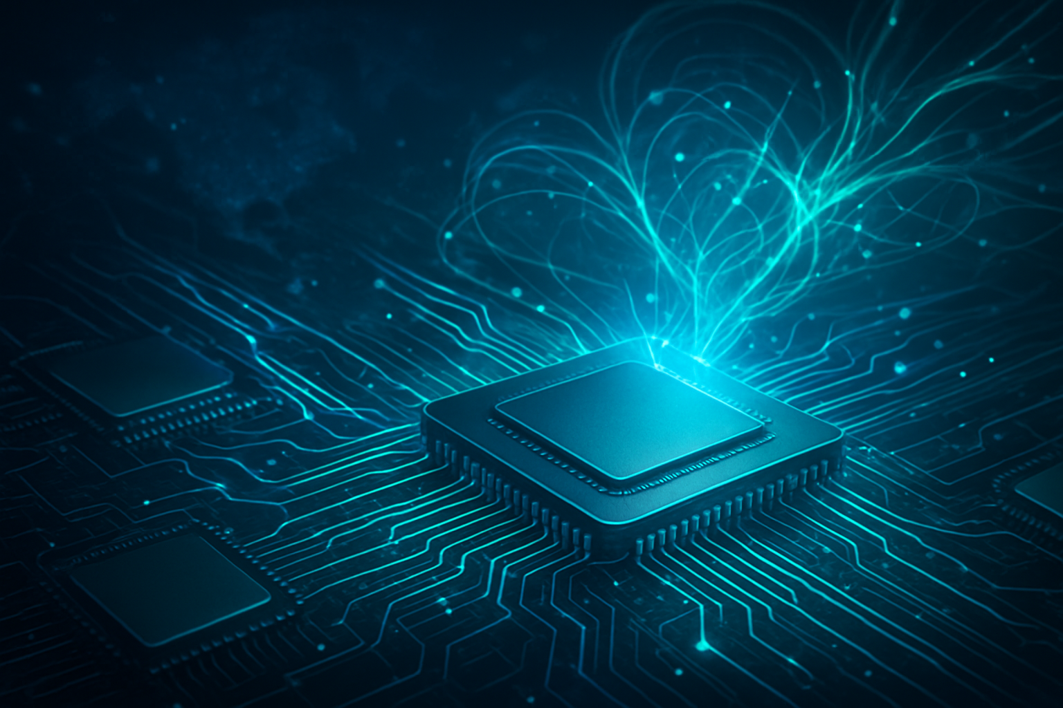
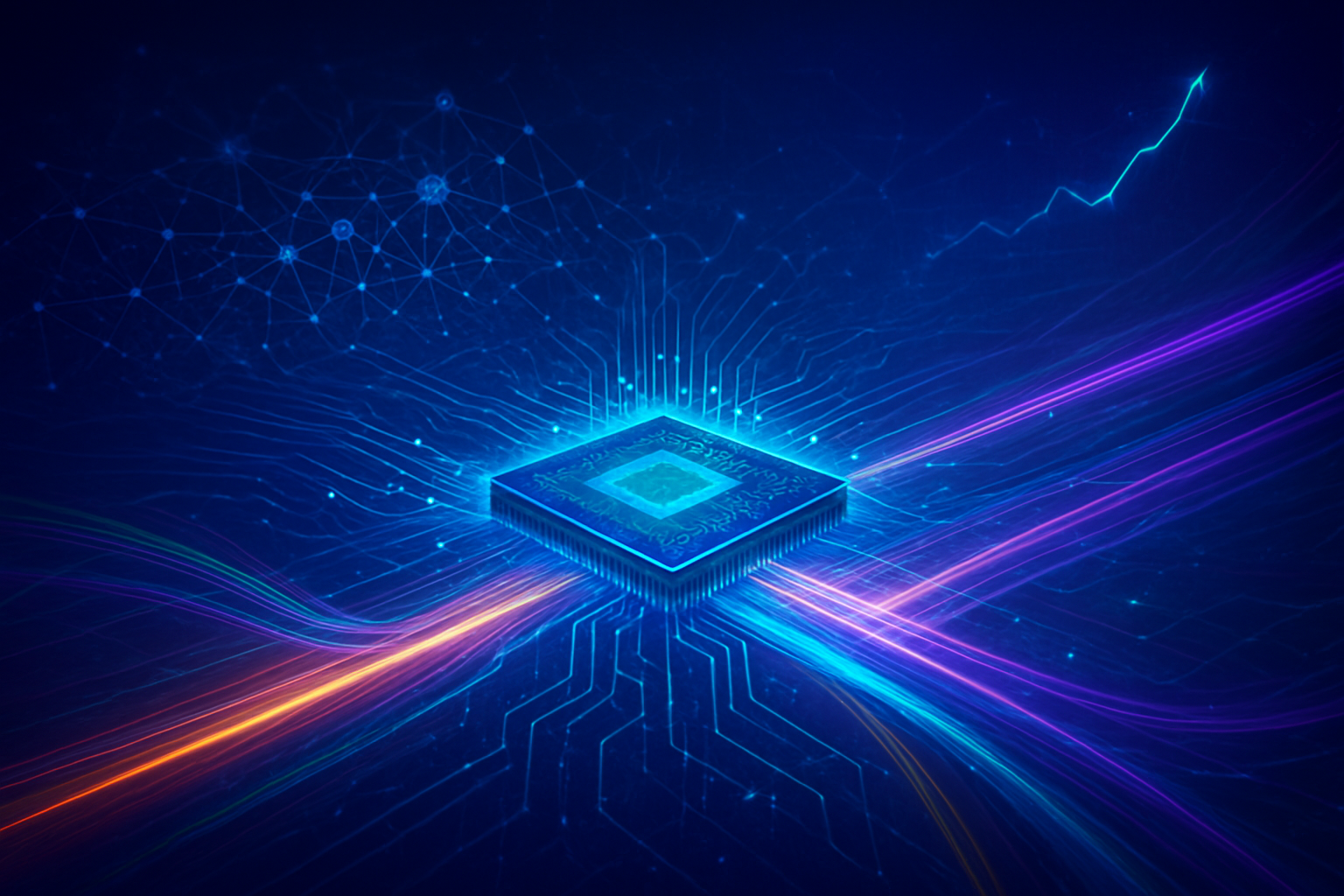
    Technical Prowess Driving AI Innovation

    Tower Semiconductor's success is deeply rooted in its advanced analog process technologies, primarily Silicon Photonics (SiPho) and Silicon Germanium (SiGe) BiCMOS, which offer distinct advantages for AI and data center applications. These specialized platforms provide high-performance, low-power, and cost-effective solutions that differentiate Tower in a highly competitive market.

    The company's SiPho platform, notably the PH18 offering, is engineered for high-volume photonics foundry applications, crucial for data center interconnects and high-performance computing. Key technical features include low-loss silicon and silicon nitride waveguides, integrated Germanium PIN diodes, Mach-Zehnder Modulators (MZMs), and efficient on-chip heater elements. A significant innovation is its ability to offer under-bump metallization for laser attachment and on-chip integrated III-V material laser options, with plans for further integrated laser solutions through partnerships. This capability drastically reduces the number of external optical components, effectively halving the lasers required per module, simplifying design, and improving cost and supply chain efficiency. Tower's latest SiPho platform supports an impressive 200 Gigabits per second (Gbps) per lane, enabling 1.6 Terabits per second (Tbps) products and a clear roadmap to 400Gbps per lane (3.2T) optical modules. This open platform, unlike some proprietary alternatives, fosters broader innovation and accessibility.

    Complementing SiPho, Tower's SiGe BiCMOS platform is optimized for high-frequency wireless communications and high-speed networking. Featuring SiGe HBT transistors with Ft/Fmax speeds exceeding 340/450 GHz, it offers ultra-low noise and high linearity, essential for RF applications. Available in various CMOS nodes (0.35µm to 65nm), it allows for high levels of mixed-signal and logic integration. This technology is ideal for optical fiber transceiver components such as Trans-impedance Amplifiers (TIAs), Laser Drivers (LDs), Limiting Amplifiers (LAs), and Clock Data Recoveries (CDRs) for data rates up to 400Gb/s and beyond, with its SBC18H5 technology now being adopted for next-generation 800 Gb/s data networks. The combined strength of SiPho and SiGe provides a comprehensive solution for the expanding data communication market, offering both optical components and fast electronic devices. Initial reactions from the AI research community and industry experts have been overwhelmingly positive, with significant demand reported for both SiPho and SiGe technologies. Analysts view Tower's leadership in these specialized areas as a competitive advantage over larger general-purpose foundries, acknowledging the critical role these technologies play in the transition to 800G and 1.6T generations of data center connectivity.

    Reshaping the AI and Tech Landscape

    Tower Semiconductor's (NASDAQ: TSEM) expansion into AI-focused production is poised to significantly influence the entire tech industry, from nascent AI startups to established tech giants. Its specialized SiPho and SiGe technologies offer enhanced cost-efficiency, simplified design, and increased scalability, directly benefiting companies that rely on high-speed, energy-efficient data processing.

    Hyperscale data center operators and cloud providers, often major tech giants, stand to gain immensely from the cost-efficient, high-performance optical connectivity enabled by Tower's SiPho solutions. By reducing the number of external optical components and simplifying module design, Tower helps these companies optimize their massive and growing AI-driven data centers. A prime beneficiary is Innolight, a global leader in high-speed optical transceivers, which has expanded its partnership with Tower to leverage the SiPho platform for mass production of next-generation optical modules (400G/800G, 1.6T, and future 3.2T). This collaboration provides Innolight with superior performance, cost efficiency, and supply chain resilience for its hyperscale customers. Furthermore, collaborations with companies like AIStorm, which integrates AI capabilities directly into high-speed imaging sensors using Tower's charge-domain imaging platform, are enabling advanced AI at the edge for applications such as robotics and industrial automation, opening new avenues for specialized AI startups.

    The competitive implications for major AI labs and tech companies are substantial. Tower's advancements in SiPho will intensify competition in the high-speed optical transceiver market, compelling other players to innovate. By offering specialized foundry services, Tower empowers AI companies to develop custom AI accelerators and infrastructure components optimized for specific AI workloads, potentially diversifying the AI hardware landscape beyond a few dominant GPU suppliers. This specialization provides a strategic advantage for those partnering with Tower, allowing for a more tailored approach to AI hardware. While Tower primarily operates in analog and specialty process technologies, complementing rather than directly competing with leading-edge digital foundries like TSMC (NYSE: TSM) and Samsung Foundry (KRX: 005930), its collaboration with Intel (NASDAQ: INTC) for 300mm manufacturing capacity for advanced analog processing highlights a synergistic dynamic, expanding Tower's reach while providing Intel Foundry Services with a significant customer. The potential disruption lies in the fundamental shift towards more compact, energy-efficient, and cost-effective optical interconnect solutions for AI data centers, which could fundamentally alter how data centers are built and scaled.

    A Crucial Pillar in the AI Supercycle

    Tower Semiconductor's (NASDAQ: TSEM) expansion is a timely and critical development, perfectly aligned with the broader AI landscape's relentless demand for high-speed, energy-efficient data processing. This move firmly embeds Tower as a crucial pillar in what experts are calling the "AI supercycle," a period characterized by unprecedented acceleration in AI development and a distinct focus on specialized AI acceleration hardware.

    The integration of SiPho and SiGe technologies directly addresses the escalating need for ultra-high bandwidth and low-latency communication in AI and machine learning (ML) applications. As AI models, particularly large language models (LLMs) and generative AI, grow exponentially in complexity, traditional electrical interconnects are becoming bottlenecks. SiPho, by leveraging light for data transmission, offers a scalable solution that significantly enhances performance and energy efficiency in large-scale AI clusters, moving beyond the "memory wall" challenge. Similarly, SiGe BiCMOS is vital for the high-frequency and RF infrastructure of AI-driven data centers and 5G telecom networks, supporting ultra-high-speed data communications and specialized analog computation. This emphasis on specialized hardware and advanced packaging, where multiple chips or chiplets are integrated to boost performance and power efficiency, marks a significant evolution from earlier AI hardware approaches, which were often constrained by general-purpose processors.

    The wider impacts of this development are profound. By providing the foundational hardware for faster and more efficient AI computations, Tower is directly accelerating breakthroughs in AI capabilities and applications. This will transform data centers and cloud infrastructure, enabling more powerful and responsive AI services while addressing the sustainability concerns of energy-intensive AI processing. New AI applications, from sophisticated autonomous vehicles with AI-driven LiDAR to neuromorphic computing, will become more feasible. Economically, companies like Tower, investing in these critical technologies, are poised for significant market share in the rapidly growing global AI hardware market. However, concerns persist, including the massive capital investments required for advanced fabs and R&D, the inherent technical complexity of heterogeneous integration, and ongoing supply chain vulnerabilities. Compared to previous AI milestones, such as the transistor revolution, the rise of integrated circuits, and the widespread adoption of GPUs, the current phase, exemplified by Tower's SiPho and SiGe expansion, represents a shift towards overcoming physical and economic limits through heterogeneous integration and photonics. It signifies a move beyond purely transistor-count scaling (Moore's Law) towards building intelligence into physical systems with precision and real-world feedback, a defining characteristic of the AI supercycle.

    The Road Ahead: Powering Future AI Ecosystems

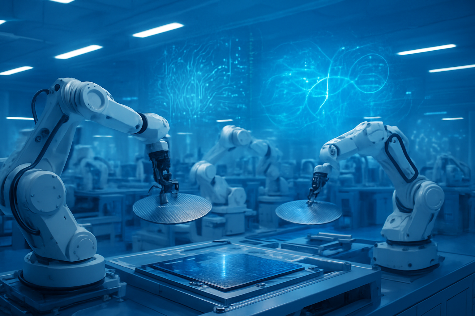
    Looking ahead, Tower Semiconductor (NASDAQ: TSEM) is poised for significant near-term and long-term developments in its AI-focused production, driven by continuous innovation in its SiPho and SiGe technologies. The company is aggressively investing an additional $300 million to $350 million to boost manufacturing capacity across its fabs in Israel, the U.S., and Japan, demonstrating a clear commitment to scaling for future AI and next-generation communications.

    Near-term, the company's newest SiPho platform is already in high-volume production, with revenue in this segment tripling in 2024 to over $100 million and expected to double again in 2025. Key developments include further advancements in reducing external optical components and a rapid transition towards co-packaged optics (CPO), where the optical interface is integrated closer to the compute. Tower's introduction of a new 300mm Silicon Photonics process as a standard foundry offering will further streamline integration with electronic components. For SiGe, the company, already a market leader in optical transceivers, is seeing its SBC18H5 technology adopted for next-generation 800 Gb/s data networks, with a clear roadmap to support even higher data rates. Potential new applications span beyond data centers to autonomous vehicles (AI-driven LiDAR), quantum photonic computing, neuromorphic computing, and high-speed optical I/O for accelerators, showcasing the versatile nature of these technologies.

    However, challenges remain. Tower operates in a highly competitive market, facing giants like TSMC (NYSE: TSM) and Intel (NASDAQ: INTC) who are also entering the photonics space. The company must carefully manage execution risk and ensure that its substantial capital investments translate into sustained growth amidst potential market fluctuations and an analog chip glut. Experts, nonetheless, predict a bright future, recognizing Tower's market leadership in SiGe and SiPho for optical transceivers as critical for AI and data centers. The transition to CPO and the demand for lower latency, power consumption, and increased bandwidth in AI networks will continue to fuel the demand for silicon photonics, transforming the switching layer in AI networks. Tower's specialization in high-value analog solutions and its strategic partnerships are expected to drive its success in powering the next generation of AI and data center infrastructure.

    A Defining Moment in AI Hardware Evolution

    Tower Semiconductor's (NASDAQ: TSEM) surge to a $10 billion valuation represents more than just financial success; it is a defining moment in the evolution of AI hardware. The company's strategic pivot and aggressive investment in specialized Silicon Photonics (SiPho) and Silicon Germanium (SiGe) technologies have positioned it as an indispensable enabler of the ongoing AI supercycle. The key takeaway is that specialized foundries focusing on high-performance, energy-efficient analog solutions are becoming increasingly critical for unlocking the full potential of AI.

    This development signifies a crucial shift in the AI landscape, moving beyond incremental improvements in general-purpose processors to a focus on highly integrated, specialized hardware that can overcome the physical limitations of data transfer and processing. Tower's ability to halve the number of lasers in optical modules and support multi-terabit data rates is not just a technical feat; it's a fundamental change in how AI infrastructure will be built, making it more scalable, cost-effective, and sustainable. This places Tower Semiconductor at the forefront of enabling the next generation of AI models and applications, from hyperscale data centers to the burgeoning field of edge AI.

    In the long term, Tower's innovations are expected to continue driving the industry towards a future where optical interconnects and high-frequency analog components are seamlessly integrated with digital processing units. This will pave the way for entirely new AI architectures and capabilities, further blurring the lines between computing, communication, and sensing. What to watch for in the coming weeks and months are further announcements regarding new partnerships, expanded production capacities, and the adoption of their advanced SiPho and SiGe solutions in next-generation AI accelerators and data center deployments. Tower Semiconductor's trajectory will serve as a critical indicator of the broader industry's progress in building the foundational hardware for the AI-powered future.


    This content is intended for informational purposes only and represents analysis of current AI developments.

    TokenRing AI delivers enterprise-grade solutions for multi-agent AI workflow orchestration, AI-powered development tools, and seamless remote collaboration platforms.
    For more information, visit https://www.tokenring.ai/.

  • Nvidia’s Reign Unchallenged: A Deep Dive into its Multi-Trillion Dollar AI Semiconductor Empire

    Nvidia’s Reign Unchallenged: A Deep Dive into its Multi-Trillion Dollar AI Semiconductor Empire

    Nvidia (NASDAQ: NVDA) has firmly cemented its position as the undisputed titan of the artificial intelligence (AI) semiconductor market, with its market capitalization consistently hovering in the multi-trillion dollar range as of November 2025. The company's relentless innovation in GPU technology, coupled with its pervasive CUDA software ecosystem and strategic industry partnerships, has created a formidable moat around its leadership, making it an indispensable enabler of the global AI revolution. Despite recent market fluctuations, which saw its valuation briefly surpass $5 trillion before a slight pullback, Nvidia remains one of the world's most valuable companies, underpinning virtually every major AI advancement today.

    This profound dominance is not merely a testament to superior hardware but reflects a holistic strategy that integrates cutting-edge silicon with a comprehensive software stack. Nvidia's GPUs are the computational engines powering the most sophisticated AI models, from generative AI to advanced scientific research, making the company's trajectory synonymous with the future of artificial intelligence itself.

    Blackwell: The Engine of Next-Generation AI

    Nvidia's strategic innovation pipeline continues to set new benchmarks, with the Blackwell architecture, unveiled in March 2024 and becoming widely available in late 2024 and early 2025, leading the charge. This revolutionary platform is specifically engineered to meet the escalating demands of generative AI and large language models (LLMs), representing a monumental leap over its predecessors. As of November 2025, enhanced systems like Blackwell Ultra (B300 series) are anticipated, with its successor, "Rubin," already slated for mass production in Q4 2025.

    The Blackwell architecture introduces several groundbreaking advancements. GPUs like the B200 boast a staggering 208 billion transistors, more than 2.5 times the 80 billion in Hopper H100 GPUs, achieved through a dual-die design connected by a 10 TB/s chip-to-chip interconnect. Manufactured using a custom-built TSMC 4NP process, the B200 GPU delivers up to 20 petaFLOPS (PFLOPS) of FP4 AI compute, with native support for 4-bit floating point (FP4) AI and new MXFP6 and MXFP4 microscaling formats, effectively doubling performance and model sizes. For LLM inference, Blackwell promises up to a 30x performance leap over Hopper. Memory capacity is also significantly boosted, with the B200 offering 192 GB of HBM3e and the GB300 reaching 288 GB HBM3e, compared to Hopper's 80 GB HBM3. The fifth-generation NVLink on Blackwell provides 1.8 TB/s of bidirectional bandwidth per GPU, doubling Hopper's, and enabling model parallelism across up to 576 GPUs. Furthermore, Blackwell offers up to 25 times lower energy per inference, a critical factor given the growing energy demands of large-scale LLMs, and includes a second-generation Transformer Engine and a dedicated decompression engine for accelerated data processing.

    This leap in technology sharply differentiates Blackwell from previous generations and competitors. Unlike Hopper's monolithic die, Blackwell employs a chiplet design. It introduces native FP4 precision, significantly higher AI throughput, and expanded memory. While competitors like Advanced Micro Devices (NASDAQ: AMD) with its Instinct MI300X series and Intel (NASDAQ: INTC) with its Gaudi accelerators offer compelling alternatives, particularly in terms of cost-effectiveness and market access in regions like China, Nvidia's Blackwell maintains a substantial performance lead. Initial reactions from the AI research community and industry experts have been overwhelmingly positive, with demand described as "insane" and orders reportedly sold out for the next 12 months. CEOs from major tech companies like Alphabet (NASDAQ: GOOGL), Meta Platforms (NASDAQ: META), Microsoft (NASDAQ: MSFT), OpenAI, and Oracle (NYSE: ORCL) have publicly endorsed Blackwell's capabilities, underscoring its pivotal role in advancing generative AI.

    Reshaping the AI Ecosystem: Implications for Tech Giants and Startups

    Nvidia's continued dominance with Blackwell and future architectures like Rubin is profoundly reshaping the competitive landscape for major AI companies, tech giants, and burgeoning AI startups. While Nvidia remains an indispensable supplier, its market position is simultaneously catalyzing a strategic shift towards diversification among its largest customers.

    Major AI companies and hyperscale cloud providers, including Microsoft, Amazon (NASDAQ: AMZN), Google, Meta, and OpenAI, remain massive purchasers of Nvidia's GPUs. Their reliance on Nvidia's technology is critical for powering their extensive AI services, from cloud-based AI platforms to cutting-edge research. However, this deep reliance also fuels significant investment in developing custom AI chips (ASICs). Google, for instance, has introduced its seventh-generation Tensor Processing Unit (TPU), codenamed Ironwood, which is four times faster than its predecessor, and is expanding its external supply. Microsoft has launched its custom Maia 100 AI accelerator and Cobalt 100 cloud CPU for Azure, aiming to shift a majority of its AI workloads to homegrown silicon. Similarly, Meta is testing its in-house Meta Training and Inference Accelerator (MTIA) series to reduce dependency and infrastructure costs. OpenAI, while committing to deploy millions of Nvidia GPUs, including on the future Vera Rubin platform as part of a significant strategic partnership and investment, is also collaborating with Broadcom (NASDAQ: AVGO) and AMD for custom accelerators and its own chip development.

    This trend of internal chip development presents the most significant potential disruption to Nvidia's long-term dominance. Custom chips offer advantages in cost efficiency, ecosystem integration, and workload-specific performance, and are projected to capture over 40% of the AI chip market by 2030. The high cost of Nvidia's chips further incentivizes these investments. While Nvidia continues to be the primary beneficiary of the AI boom, generating massive revenue from GPU sales, its strategic investments into its customers also secure future demand. Hyperscale cloud providers, memory and component manufacturers (like Samsung (KRX: 005930) and SK Hynix (KRX: 000660)), and Nvidia's strategic partners also stand to benefit. AI startups face a mixed bag; while they can leverage cloud providers to access powerful Nvidia GPUs without heavy capital expenditure, access to the most cutting-edge hardware might be limited due to overwhelming demand from hyperscalers.

    Broader Significance: AI's Backbone and Emerging Challenges

    Nvidia's overwhelming dominance in AI semiconductors is not just a commercial success story; it's a foundational element shaping the entire AI landscape and its broader societal implications as of November 2025. With an estimated 85% to 94% market share in the AI GPU market, Nvidia's hardware and CUDA software platform are the de facto backbone of the AI revolution, enabling unprecedented advancements in generative AI, scientific discovery, and industrial automation.

    The company's continuous innovation, with architectures like Blackwell and the upcoming Rubin, is driving the capability to process trillion-parameter models, essential for the next generation of AI. This accelerates progress across diverse fields, from predictive diagnostics in healthcare to autonomous systems and advanced climate modeling. Economically, Nvidia's success, evidenced by its multi-trillion dollar market cap and projected $49 billion in AI-related revenue for 2025, is a significant driver of the AI-driven tech rally. However, this concentration of power also raises concerns about potential monopolies and accessibility. The high switching costs associated with the CUDA ecosystem make it difficult for smaller companies to adopt alternative hardware, potentially stifling broader ecosystem development.

    Geopolitical tensions, particularly U.S. export restrictions, significantly impact Nvidia's access to the crucial Chinese market. This has led to a drastic decline in Nvidia's market share in China's data center AI accelerator market, from approximately 95% to virtually zero. This geopolitical friction is reshaping global supply chains, fostering domestic chip development in China, and creating a bifurcated global AI ecosystem. Comparing this to previous AI milestones, Nvidia's current role highlights a shift where specialized hardware infrastructure is now the primary enabler and accelerator of algorithmic advances, a departure from earlier eras where software and algorithms were often the main bottlenecks.

    The Horizon: Continuous Innovation and Mounting Challenges

    Looking ahead, Nvidia's AI semiconductor strategy promises an unrelenting pace of innovation, while the broader AI landscape faces both explosive growth and significant challenges. In the near term (late 2024 – 2025), the Blackwell architecture, including the B100, B200, and GB200 Superchip, will continue its rollout, with the Blackwell Ultra expected in the second half of 2025. Beyond 2025, the "Rubin" architecture (including R100 GPUs and Vera CPUs) is slated for release in the first half of 2026, leveraging HBM4 and TSMC's 3nm EUV FinFET process, followed by "Rubin Ultra" and "Feynman" architectures. This commitment to an annual release cadence for new chip architectures, with major updates every two years, ensures continuous performance improvements focused on transistor density, memory bandwidth, specialized cores, and energy efficiency.

    The global AI market is projected to expand significantly, with the AI chip market alone potentially exceeding $200 billion by 2030. Expected developments include advancements in quantum AI, the proliferation of small language models, and multimodal AI systems. AI is set to drive the next phase of autonomous systems, workforce transformation, and AI-driven software development. Potential applications span healthcare (predictive diagnostics, drug discovery), finance (autonomous finance, fraud detection), robotics and autonomous vehicles (Nvidia's DRIVE Hyperion platform), telecommunications (AI-native 6G networks), cybersecurity, and scientific discovery.

    However, significant challenges loom. Data quality and bias, the AI talent shortage, and the immense energy consumption of AI data centers (a single rack of Blackwell GPUs consumes 120 kilowatts) are critical hurdles. Privacy, security, and compliance concerns, along with the "black box" problem of model interpretability, demand robust solutions. Geopolitical tensions, particularly U.S. export restrictions to China, continue to reshape global AI supply chains and intensify competition from rivals like AMD and Intel, as well as custom chip development by hyperscalers. Experts predict Nvidia will likely maintain its dominance in high-end AI outside of China, but competition is expected to intensify, with custom chips from tech giants projected to capture over 40% of the market share by 2030.

    A Legacy Forged in Silicon: The AI Future Unfolds

    In summary, Nvidia's enduring dominance in the AI semiconductor market, underscored by its Blackwell architecture and an aggressive future roadmap, is a defining feature of the current AI revolution. Its unparalleled market share, formidable CUDA ecosystem, and relentless hardware innovation have made it the indispensable engine powering the world's most advanced AI systems. This leadership is not just a commercial success but a critical enabler of scientific breakthroughs, technological advancements, and economic growth across industries.

    Nvidia's significance in AI history is profound, having provided the foundational computational infrastructure that enabled the deep learning revolution. Its long-term impact will likely include standardizing AI infrastructure, accelerating innovation across the board, but also potentially creating high barriers to entry and navigating complex geopolitical landscapes. As we move forward, the successful rollout and widespread adoption of Blackwell Ultra and the upcoming Rubin architecture will be crucial. Investors will be closely watching Nvidia's financial results for continued growth, while the broader industry will monitor intensifying competition, the evolving geopolitical landscape, and the critical imperative of addressing AI's energy consumption and ethical implications. Nvidia's journey will continue to be a bellwether for the future of artificial intelligence.


    This content is intended for informational purposes only and represents analysis of current AI developments.

    TokenRing AI delivers enterprise-grade solutions for multi-agent AI workflow orchestration, AI-powered development tools, and seamless remote collaboration platforms.
    For more information, visit https://www.tokenring.ai/.

  • AI Chip Wars Escalate: Nvidia’s Blackwell Unleashes Trillion-Parameter Power as Qualcomm Enters the Data Center Fray

    AI Chip Wars Escalate: Nvidia’s Blackwell Unleashes Trillion-Parameter Power as Qualcomm Enters the Data Center Fray

    The artificial intelligence landscape is witnessing an unprecedented acceleration in hardware innovation, with two industry titans, Nvidia (NASDAQ: NVDA) and Qualcomm (NASDAQ: QCOM), spearheading the charge with their latest AI chip architectures. Nvidia's Blackwell platform, featuring the groundbreaking GB200 Grace Blackwell Superchip and fifth-generation NVLink, is already rolling out, promising up to a 30x performance leap for large language model (LLM) inference. Simultaneously, Qualcomm has officially thrown its hat into the AI data center ring with the announcement of its AI200 and AI250 chips, signaling a strategic and potent challenge to Nvidia's established dominance by focusing on power-efficient, cost-effective rack-scale AI inference.

    As of late 2024 and early 2025, these developments are not merely incremental upgrades but represent foundational shifts in how AI models will be trained, deployed, and scaled. Nvidia's Blackwell is poised to solidify its leadership in high-end AI training and inference, catering to the insatiable demand from hyperscalers and major AI labs. Meanwhile, Qualcomm's strategic entry, though with commercial availability slated for 2026 and 2027, has already sent ripples through the market, promising a future of intensified competition, diverse choices for enterprises, and potentially lower total cost of ownership for deploying generative AI at scale. The immediate impact is a palpable surge in AI processing capabilities, setting the stage for more complex, efficient, and accessible AI applications across industries.

    A Technical Deep Dive into Next-Generation AI Architectures

    Nvidia's Blackwell architecture, named after the pioneering mathematician David Blackwell, represents a monumental leap in GPU design, engineered to power the next generation of AI and accelerated computing. At its core is the Blackwell GPU, the largest ever produced by Nvidia, boasting an astonishing 208 billion transistors fabricated on TSMC's custom 4NP process. This GPU employs an innovative dual-die design, where two massive dies function cohesively as a single unit, interconnected by a blazing-fast 10 TB/s NV-HBI interface. A single Blackwell GPU can deliver up to 20 petaFLOPS of FP4 compute power. The true powerhouse, however, is the GB200 Grace Blackwell Superchip, which integrates two Blackwell Tensor Core GPUs with an Nvidia Grace CPU, leveraging NVLink-C2C for 900 GB/s bidirectional bandwidth. This integration, along with 192 GB of HBM3e memory providing 8 TB/s bandwidth per B200 GPU, sets a new standard for memory-intensive AI workloads.

    A cornerstone of Blackwell's scalability is the fifth-generation NVLink, which doubles the bandwidth of its predecessor to 1.8 TB/s bidirectional throughput per GPU. This allows for seamless, high-speed communication across an astounding 576 GPUs, a necessity for training and deploying trillion-parameter AI models. The NVLink Switch further extends this interconnect across multiple servers, enabling model parallelism across vast GPU clusters. The flagship GB200 NVL72 is a liquid-cooled, rack-scale system comprising 36 GB200 Superchips, effectively creating a single, massive GPU cluster capable of 1.44 exaFLOPS (FP4) of compute performance. Blackwell also introduces a second-generation Transformer Engine that accelerates LLM inference and training, supporting new precisions like 8-bit floating point (FP8) and a novel 4-bit floating point (NVFP4) format, while leveraging advanced dynamic range management for accuracy. This architecture offers a staggering 30 times faster real-time inference for trillion-parameter LLMs and 4 times faster training compared to H100-based systems, all while reducing energy consumption per inference by up to 25 times.

    In stark contrast, Qualcomm's AI200 and AI250 chips are purpose-built for rack-scale AI inference in data centers, with a strong emphasis on power efficiency, cost-effectiveness, and memory capacity for generative AI. While Nvidia targets the full spectrum of AI, from training to inference at the highest scale, Qualcomm strategically aims to disrupt the burgeoning inference market. The AI200 and AI250 chips leverage Qualcomm's deep expertise in mobile NPU technology, incorporating the Qualcomm AI Engine which includes the Hexagon NPU, Adreno GPU, and Kryo/Oryon CPU. A standout innovation in the AI250 is its "near-memory computing" (NMC) architecture, which Qualcomm claims delivers over 10 times the effective memory bandwidth and significantly lower power consumption by minimizing data movement.

    Both the AI200 and AI250 utilize high-capacity LPDDR memory, with the AI200 supporting an impressive 768 GB per card. This choice of LPDDR provides greater memory capacity at a lower cost, crucial for the memory-intensive requirements of large language models and multimodal models, especially for large-context-window applications. Qualcomm's focus is on optimizing performance per dollar per watt, aiming to drastically reduce the total cost of ownership (TCO) for data centers. Their rack solutions feature direct liquid cooling and are designed for both scale-up (PCIe) and scale-out (Ethernet) capabilities. The AI research community and industry experts have largely applauded Nvidia's Blackwell as a continuation of its technological dominance, solidifying its "strategic moat" with CUDA and continuous innovation. Qualcomm's entry, while not yet delivering commercially available chips, is viewed as a bold and credible challenge, with its focus on TCO and power efficiency offering a compelling alternative for enterprises, potentially diversifying the AI hardware landscape and intensifying competition.

    Industry Impact: Shifting Sands in the AI Hardware Arena

    The introduction of Nvidia's Blackwell and Qualcomm's AI200/AI250 chips is poised to reshape the competitive landscape for AI companies, tech giants, and startups alike. Nvidia's (NASDAQ: NVDA) Blackwell platform, with its unprecedented performance gains and scalability, primarily benefits hyperscale cloud providers like Microsoft (NASDAQ: MSFT), Amazon (NASDAQ: AMZN), Google (NASDAQ: GOOGL), and Meta (NASDAQ: META), who are at the forefront of AI model development and deployment. These companies, already Nvidia's largest customers, will leverage Blackwell to train even larger and more complex models, accelerating their AI research and product roadmaps. Server makers and leading AI companies also stand to gain immensely from the increased throughput and energy efficiency, allowing them to offer more powerful and cost-effective AI services. This solidifies Nvidia's strategic advantage in the high-end AI training market, particularly outside of China due to export restrictions, ensuring its continued leadership in the AI supercycle.

    Qualcomm's (NASDAQ: QCOM) strategic entry into the data center AI inference market with the AI200/AI250 chips presents a significant competitive implication. While Nvidia has a strong hold on both training and inference, Qualcomm is directly targeting the rapidly expanding AI inference segment, which is expected to constitute a larger portion of AI workloads in the future. Qualcomm's emphasis on power efficiency, lower total cost of ownership (TCO), and high memory capacity through LPDDR memory and near-memory computing offers a compelling alternative for enterprises and cloud providers looking to deploy generative AI at scale more economically. This could disrupt existing inference solutions by providing a more cost-effective and energy-efficient option, potentially leading to a more diversified supplier base and reduced reliance on a single vendor.

    The competitive implications extend beyond just Nvidia and Qualcomm. Other AI chip developers, such as AMD (NASDAQ: AMD), Intel (NASDAQ: INTC), and various startups, will face increased pressure to innovate and differentiate their offerings. Qualcomm's move signals a broader trend of specialized hardware for AI workloads, potentially leading to a more fragmented but ultimately more efficient market. Companies that can effectively integrate these new chip architectures into their existing infrastructure or develop new services leveraging their unique capabilities will gain significant market positioning and strategic advantages. The potential for lower inference costs could also democratize access to advanced AI, enabling a wider range of startups and smaller enterprises to deploy sophisticated AI models without prohibitive hardware expenses, thereby fostering further innovation across the industry.

    Wider Significance: Reshaping the AI Landscape and Addressing Grand Challenges

    The introduction of Nvidia's Blackwell and Qualcomm's AI200/AI250 chips signifies a profound evolution in the broader AI landscape, addressing critical trends such as the relentless pursuit of larger AI models, the urgent need for energy efficiency, and the ongoing efforts towards the democratization of AI. Nvidia's Blackwell architecture, with its capability to handle trillion-parameter and multi-trillion-parameter models, is explicitly designed to be the cornerstone for the next era of high-performance AI infrastructure. This directly accelerates the development and deployment of increasingly complex generative AI, data analytics, and high-performance computing (HPC) workloads, pushing the boundaries of what AI can achieve. Its superior processing speed and efficiency also tackle the growing concern of AI's energy footprint; Nvidia highlights that training ultra-large AI models with 2,000 Blackwell GPUs would consume 4 megawatts over 90 days, a stark contrast to 15 megawatts for 8,000 older GPUs, demonstrating a significant leap in power efficiency.

    Qualcomm's AI200/AI250 chips, while focused on inference, also contribute significantly to these trends. By prioritizing power efficiency and a lower Total Cost of Ownership (TCO), Qualcomm aims to democratize access to high-performance AI inference, challenging the traditional reliance on general-purpose GPUs for all AI workloads. Their architecture, optimized for running large language models (LLMs) and multimodal models (LMMs) efficiently, is crucial for the increasing demand for real-time generative AI applications in data centers. The AI250's near-memory computing architecture, promising over 10 times higher effective memory bandwidth and significantly reduced power consumption, directly addresses the memory wall problem and the escalating energy demands of AI. Both companies, through their distinct approaches, are enabling the continued growth of sophisticated generative AI models, addressing the critical need for energy efficiency, and striving to make powerful AI capabilities more accessible.

    However, these advancements are not without potential concerns. The sheer computational power and high-density designs of these new chips translate to substantial power requirements. High-density racks with Blackwell GPUs, for instance, can demand 60kW to 120kW, and Qualcomm's racks draw 160 kW, necessitating advanced cooling solutions like liquid cooling. This stresses existing electrical grids and raises significant environmental questions. The cutting-edge nature and performance also come with a high price tag, potentially creating an "AI divide" where smaller research groups and startups might struggle to access these transformative technologies. Furthermore, Nvidia's robust CUDA software ecosystem, while a major strength, can contribute to vendor lock-in, posing a challenge for competitors and hindering diversification in the AI software stack. Geopolitical factors, such as export controls on advanced semiconductors, also loom large, impacting global availability and adoption.

    Comparing these to previous AI milestones reveals both evolutionary and revolutionary steps. Blackwell represents a dramatic extension of previous GPU generations like Hopper and Ampere, introducing FP4 precision and a second-generation Transformer Engine specifically to tackle the scaling challenges of modern LLMs, which were not as prominent in earlier designs. The emphasis on massive multi-GPU scaling with enhanced NVLink for trillion-parameter models pushes boundaries far beyond what was feasible even a few years ago. Qualcomm's entry as an inference specialist, leveraging its mobile NPU heritage, marks a significant diversification of the AI chip market. This specialization, reminiscent of Google's Tensor Processing Units (TPUs), signals a maturing AI hardware market where dedicated solutions can offer substantial advantages in TCO and efficiency for production deployment, challenging the GPU's sole dominance in certain segments. Both companies' move towards delivering integrated, rack-scale AI systems, rather than just individual chips, also reflects the immense computational and communication demands of today's AI workloads, marking a new era in AI infrastructure development.

    Future Developments: The Road Ahead for AI Silicon

    The trajectory of AI chip architecture is one of relentless innovation, with both Nvidia and Qualcomm already charting ambitious roadmaps that extend far beyond their current offerings. For Nvidia (NASDAQ: NVDA), the Blackwell platform, while revolutionary, is just a stepping stone. The near-term will see the release of Blackwell Ultra (B300 series) in the second half of 2025, promising enhanced compute performance and a significant boost to 288GB of HBM3E memory. Nvidia has committed to an annual release cadence for its data center platforms, with major new architectures every two years and "Ultra" updates in between, ensuring a continuous stream of advancements. These chips are set to drive massive investments in data centers and cloud infrastructure, accelerating generative AI, scientific computing, advanced manufacturing, and large-scale simulations, forming the backbone of future "AI factories" and agentic AI platforms.

    Looking further ahead, Nvidia's next-generation architecture, Rubin, named after astrophysicist Vera Rubin, is already in the pipeline. The Rubin GPU and its companion CPU, Vera, are scheduled for mass production in late 2025 and will be available in early 2026. Manufactured by TSMC using a 3nm process node and featuring HBM4 memory, Rubin is projected to offer 50 petaflops of performance in FP4, a substantial increase from Blackwell's 20 petaflops. An even more powerful Rubin Ultra is planned for 2027, expected to double Rubin's performance to 100 petaflops and deliver up to 15 ExaFLOPS of FP4 inference compute in a full rack configuration. Rubin will also incorporate NVLink 6 switches (3600 GB/s) and CX9 network cards (1,600 Gb/s) to support unprecedented data transfer needs. Experts predict Rubin will be a significant step towards Artificial General Intelligence (AGI) and is already slated for use in supercomputers like Los Alamos National Laboratory's Mission and Vision systems. Challenges for Nvidia include navigating geopolitical tensions and export controls, maintaining its technological lead through continuous R&D, and addressing the escalating power and cooling demands of "gigawatt AI factories."

    Qualcomm (NASDAQ: QCOM), while entering the data center market with the AI200 (commercial availability in 2026) and AI250 (2027), also has a clear and aggressive strategic roadmap. The AI200 will support 768GB of LPDDR memory per card for cost-effective, high-capacity inference. The AI250 will introduce an innovative near-memory computing architecture, promising over 10 times higher effective memory bandwidth and significantly lower power consumption, marking a generational leap in efficiency for AI inference workloads. Qualcomm is committed to an annual cadence for its data center roadmap, focusing on industry-leading AI inference performance, energy efficiency, and total cost of ownership (TCO). These chips are primarily optimized for demanding inference workloads such as large language models, multimodal models, and generative AI tools. Early deployments include a partnership with Saudi Arabia's Humain, which plans to deploy 200 megawatts of data center racks powered by AI200 chips starting in 2026.

    Qualcomm's broader AI strategy aims for "intelligent computing everywhere," extending beyond data centers to encompass hybrid, personalized, and agentic AI across mobile, PC, wearables, and automotive devices. This involves always-on sensing and personalized knowledge graphs to enable proactive, contextually-aware AI assistants. The main challenges for Qualcomm include overcoming Nvidia's entrenched market dominance (currently over 90%), clearly validating its promised performance and efficiency gains, and building a robust developer ecosystem comparable to Nvidia's CUDA. However, experts like Qualcomm CEO Cristiano Amon believe the AI market is rapidly becoming competitive, and companies investing in efficient architectures will be well-positioned for the long term. The long-term future of AI chip architectures will likely be a hybrid landscape, utilizing a mixture of GPUs, ASICs, FPGAs, and entirely new chip architectures tailored to specific AI workloads, with innovations like silicon photonics and continued emphasis on disaggregated compute and memory resources driving efficiency and bandwidth gains. The global AI chip market is projected to reach US$257.6 billion by 2033, underscoring the immense investment and innovation yet to come.

    Comprehensive Wrap-up: A New Era of AI Silicon

    The advent of Nvidia's Blackwell and Qualcomm's AI200/AI250 chips marks a pivotal moment in the evolution of artificial intelligence hardware. Nvidia's Blackwell platform, with its GB200 Grace Blackwell Superchip and fifth-generation NVLink, is a testament to the pursuit of extreme-scale AI, delivering unprecedented performance and efficiency for trillion-parameter models. Its 208 billion transistors, advanced Transformer Engine, and rack-scale system architecture are designed to power the most demanding AI training and inference workloads, solidifying Nvidia's (NASDAQ: NVDA) position as the dominant force in high-performance AI. In parallel, Qualcomm's (NASDAQ: QCOM) AI200/AI250 chips represent a strategic and ambitious entry into the data center AI inference market, leveraging the company's mobile DNA to offer highly energy-efficient and cost-effective solutions for large language models and multimodal inference at scale.

    Historically, Nvidia's journey from gaming GPUs to the foundational CUDA platform and now Blackwell, has consistently driven the advancements in deep learning. Blackwell is not just an upgrade; it's engineered for the "generative AI era," explicitly tackling the scale and complexity that define today's AI breakthroughs. Qualcomm's AI200/AI250, building on its Cloud AI 100 Ultra lineage, signifies a crucial diversification beyond its traditional smartphone market, positioning itself as a formidable contender in the rapidly expanding AI inference segment. This shift is historically significant as it introduces a powerful alternative focused on sustainability and economic efficiency, challenging the long-standing dominance of general-purpose GPUs across all AI workloads.

    The long-term impact of these architectures will likely see a bifurcated but symbiotic AI hardware ecosystem. Blackwell will continue to drive the cutting edge of AI research, enabling the training of ever-larger and more complex models, fueling unprecedented capital expenditure from hyperscalers and sovereign AI initiatives. Its continuous innovation cycle, with the Rubin architecture already on the horizon, ensures Nvidia will remain at the forefront of AI computing. Qualcomm's AI200/AI250, conversely, could fundamentally reshape the AI inference landscape. By offering a compelling alternative that prioritizes sustainability and economic efficiency, it addresses the critical need for cost-effective, widespread AI deployment. As AI becomes ubiquitous, the sheer volume of inference tasks will demand highly efficient solutions, where Qualcomm's offerings could gain significant traction, diversifying the competitive landscape and making AI more accessible and sustainable.

    In the coming weeks and months, several key indicators will reveal the trajectory of these innovations. For Nvidia Blackwell, watch for updates in upcoming earnings reports (such as Q3 FY2026, scheduled for November 19, 2025) regarding the Blackwell Ultra ramp and overall AI infrastructure backlog. The adoption rates by major hyperscalers and sovereign AI initiatives, alongside any further developments on "downgraded" Blackwell variants for the Chinese market, will be crucial. For Qualcomm AI200/AI250, the focus will be on official shipping announcements and initial deployment reports, particularly the success of partnerships with companies like Hewlett Packard Enterprise (HPE) and Core42. Crucially, independent benchmarks and MLPerf results will be vital to validate Qualcomm's claims regarding capacity, energy efficiency, and TCO, shaping its competitive standing against Nvidia's inference offerings. Both companies' ongoing development of their AI software ecosystems and any new product roadmap announcements will also be critical for developer adoption and future market dynamics.


    This content is intended for informational purposes only and represents analysis of current AI developments.

    TokenRing AI delivers enterprise-grade solutions for multi-agent AI workflow orchestration, AI-powered development tools, and seamless remote collaboration platforms.
    For more information, visit https://www.tokenring.ai/.

  • India’s Semiconductor Dawn: Tata Electronics Plant in Assam Poised to Reshape Global Tech Landscape

    India’s Semiconductor Dawn: Tata Electronics Plant in Assam Poised to Reshape Global Tech Landscape

    GUWAHATI, ASSAM – November 7, 2025 – In a monumental stride towards technological self-reliance, India today witnessed Union Finance Minister Nirmala Sitharaman's pivotal visit to the new Tata Electronics semiconductor manufacturing facility in Jagiroad, Assam. This state-of-the-art Outsourced Semiconductor Assembly and Test (OSAT) unit, backed by an investment of INR 27,000 crore (approximately US$3.6 billion), is not merely a factory; it is a declaration of intent, positioning India at the heart of the global semiconductor supply chain and promising to ignite an economic transformation in the country's North-Eastern region. The facility, currently under construction, is on track for its first phase of operations by mid-2025, with full-scale production slated for 2026, marking a critical juncture in India's journey to becoming a formidable player in high-tech manufacturing.

    The significance of this project reverberated through Minister Sitharaman's remarks during her review of the advanced facility. She hailed the initiative as the "driver of the engine for Viksit Bharat" (Developed India) and a "golden moment" for Assam, underscoring its alignment with Prime Minister Narendra Modi's vision of a self-reliant India and the holistic development of the North-Eastern region. The establishment of such a high-value manufacturing unit is expected to dramatically reduce India's historical dependence on imported chips, fortifying its economic and strategic resilience in an increasingly digitized world.

    A Deep Dive into India's Semiconductor Ambition

    The Tata Electronics (a subsidiary of the Tata Group, represented by public entities like Tata Motors (NSE: TATAMOTORS)) facility in Assam is designed as an advanced OSAT unit, focusing on the critical stages of semiconductor manufacturing: assembly and testing. This involves taking silicon wafers produced elsewhere and transforming them into finished, functional chips through sophisticated packaging techniques. The plant will leverage three cutting-edge platform technologies: Wire Bond, Flip Chip, and Integrated Systems Packaging (ISP). These technologies are crucial for creating high-performance, compact, and reliable semiconductor components essential for modern electronics.

    Unlike traditional chip fabrication (fabs), which involves the complex and capital-intensive process of wafer manufacturing, the OSAT unit specializes in the subsequent, equally vital steps of packaging and testing. This strategic focus allows India to rapidly build capabilities in a high-value segment of the semiconductor supply chain that is currently dominated by a few global players. The semiconductors processed here will be integral to a vast array of applications, including the rapidly expanding electric vehicle (EV) sector, mobile devices, artificial intelligence (AI) hardware, advanced communications infrastructure, industrial automation, and diverse consumer electronics. Once fully operational, the facility boasts an impressive capacity to produce up to 48 million semiconductor chips daily, a testament to its scale and ambition. This indigenous capability is a stark departure from previous approaches, where India primarily served as a consumer market, and represents a significant leap in its technological maturity. Initial reactions from the domestic tech community have been overwhelmingly positive, viewing it as a watershed moment for India's manufacturing prowess.

    Reshaping the Indian and Global Tech Landscape

    The establishment of the Tata Electronics semiconductor plant is poised to have a profound impact on various stakeholders, from major tech giants to emerging startups. For the Tata Group itself, this venture marks a significant diversification and strengthening of its industrial portfolio, positioning it as a key player in a strategically vital sector. The project is expected to attract a global ecosystem to India, fostering the development of cutting-edge technologies and advanced skill sets within the country. Tata Group Chairman N Chandrasekaran had previously indicated plans to sign Memoranda of Understanding (MoUs) with ten additional semiconductor companies, signaling a concerted effort to build a robust ancillary ecosystem around the Assam facility.

    This development presents competitive implications for existing global semiconductor players by offering a new, geographically diversified manufacturing hub. While not directly competing with established fabrication giants, the OSAT facility provides an alternative for packaging and testing services, potentially reducing lead times and supply chain risks for companies worldwide. Indian tech startups, particularly those in AI, IoT, and automotive electronics, stand to benefit immensely from the domestic availability of advanced semiconductor components, enabling faster prototyping, reduced import costs, and greater innovation. The plant’s existence could also disrupt existing product development cycles by providing a localized, efficient supply of critical components, encouraging more companies to design and manufacture within India, thus enhancing the nation's market positioning and strategic advantages in the global tech arena.

    Broader Implications and Global Supply Chain Resilience

    The Tata Electronics facility in Assam fits seamlessly into the broader global trend of diversifying semiconductor manufacturing away from concentrated hubs, a strategy increasingly prioritized in the wake of geopolitical tensions and recent supply chain disruptions. By establishing significant OSAT capabilities, India is actively contributing to de-risking the global tech supply chain, offering an alternative production base that enhances resilience and reduces the world's reliance on a few key regions, particularly in East Asia. This move solidifies India's commitment to becoming a reliable and integral part of the global technology ecosystem, moving beyond its traditional role as a software and services powerhouse to a hardware manufacturing hub.

    The economic impacts on Assam and the wider North-Eastern region are anticipated to be transformative. The INR 27,000 crore investment is projected to create over 27,000 direct and indirect jobs, providing substantial employment opportunities and fostering economic diversification in a region traditionally reliant on agriculture and tea. Beyond direct employment, the project necessitates and stimulates significant infrastructure development, including improved roads, utilities, and an "electronic city" designed to house approximately 40,000 employees. The Government of Assam's commitment of a Rs 111 crore Water Supply Project further underscores the holistic development around the plant. This industrialization is expected to spawn numerous peripheral industries, creating a vibrant local business ecosystem and positioning the Northeast as a key driver in India's technology-driven growth narrative, comparable to how previous industrial milestones have reshaped other regions.

    The Road Ahead: Future Developments and Challenges

    With the first phase of the Tata Electronics plant expected to be operational by mid-2025 and full production by 2026, the near-term focus will be on ramping up operations, ensuring quality control, and integrating seamlessly into global supply chains. Experts predict that the success of this initial venture could pave the way for further significant investments in India's semiconductor ecosystem, potentially including more advanced fabrication units in the long term. The plant's focus on advanced packaging technologies like Wire Bond, Flip Chip, and ISP suggests a pathway towards even more sophisticated packaging solutions in the future, keeping pace with evolving global demands.

    However, challenges remain. Developing a highly skilled workforce capable of operating and maintaining such advanced facilities will be crucial, necessitating robust training programs and educational initiatives. Maintaining a technological edge in a rapidly evolving industry will also require continuous investment in research and development. What experts predict next is a domino effect: the establishment of this anchor unit is expected to attract more foreign direct investment into India's semiconductor sector, fostering a complete ecosystem from design to manufacturing and testing. Potential applications and use cases on the horizon include specialized chips for India's burgeoning space and defense sectors, further cementing the nation's strategic autonomy.

    A New Chapter in India's Industrial History

    The Tata Electronics semiconductor manufacturing facility in Assam represents a pivotal moment in India's industrial and technological history. It is a bold statement of intent, signaling India's ambition to move beyond being a consumer of technology to a significant producer, capable of meeting both domestic and global demands for critical electronic components. The substantial investment, coupled with the promise of thousands of jobs and comprehensive regional development, underscores the project's multifaceted significance.

    As the facility moves from construction to operationalization in the coming months, the world will be watching. The success of this venture will not only bolster India's self-reliance in a strategically vital sector but also contribute significantly to the diversification and resilience of the global tech supply chain. Key takeaways include India's commitment to indigenous manufacturing, the transformative economic potential for the North-East, and the strategic importance of semiconductor independence. The coming weeks and months will be crucial as the plant approaches its operational milestones, with further partnerships and ecosystem developments expected to unfold, cementing India's place on the global semiconductor map.


    This content is intended for informational purposes only and represents analysis of current AI developments.

    TokenRing AI delivers enterprise-grade solutions for multi-agent AI workflow orchestration, AI-powered development tools, and seamless remote collaboration platforms.
    For more information, visit https://www.tokenring.ai/.

  • Truist Securities Elevates MACOM Technology Solutions Price Target to $180 Amidst Strong Performance and Robust Outlook

    Truist Securities Elevates MACOM Technology Solutions Price Target to $180 Amidst Strong Performance and Robust Outlook

    New York, NY – November 6, 2025 – In a significant vote of confidence for the semiconductor industry, Truist Securities today announced an upward revision of its price target for MACOM Technology Solutions (NASDAQ:MTSI) shares, increasing it from $158.00 to $180.00. The investment bank also reiterated its "Buy" rating for the company, signaling a strong belief in MACOM's continued growth trajectory and market leadership. This move comes on the heels of MACOM's impressive financial performance and an optimistic outlook for the coming fiscal year, providing a clear indicator of the company's robust health within a dynamic technological landscape.

    The immediate significance of Truist's updated target underscores MACOM's solid operational execution and its ability to navigate complex market conditions. For investors, this adjustment translates into a positive signal regarding the company's intrinsic value and future earnings potential. The decision by a prominent financial institution like Truist Securities to not only maintain a "Buy" rating but also substantially increase its price target suggests a deep-seated confidence in MACOM's strategic direction, product portfolio, and its capacity to capitalize on emerging opportunities in the high-performance analog and mixed-signal semiconductor markets.

    Unpacking the Financial and Operational Drivers Behind the Upgrade

    Truist Securities' decision to elevate MACOM's price target is rooted in a comprehensive analysis of the company's recent financial disclosures and future projections. A primary driver was MACOM's strong third-quarter results, which laid the groundwork for a highly positive outlook for the fourth quarter. This consistent performance highlights the company's operational efficiency and its ability to meet or exceed market expectations in a competitive sector.

    Crucially, the upgrade acknowledges significant improvements in MACOM's gross profit margin, a key metric indicating the company's profitability. These improvements have effectively mitigated prior challenges associated with the recently acquired RTP fabrication facility, demonstrating MACOM's successful integration and optimization efforts. With a healthy gross profit margin of 54.76% and an impressive 33.5% revenue growth over the last twelve months, MACOM is showcasing a robust financial foundation that sets it apart from many peers.

    Looking ahead, Truist's analysis points to a robust early 2026 outlook for MACOM, aligning with the firm's existing model that projects a formidable $4.51 earnings per share (EPS) for calendar year 2026. The new $180 price target itself is based on a 40x multiple, which incorporates a notable 12x premium over recently elevated peers in the sector. Truist justified this premium by highlighting MACOM's consistent execution, its solid baseline growth trajectory, and significant potential upside across its various end markets, including data center, telecom, and industrial applications. Furthermore, the company's fourth-quarter earnings for fiscal year 2025 surpassed expectations, achieving an adjusted EPS of $0.94 against a forecasted $0.929, and revenue of $261.2 million, slightly above the anticipated $260.17 million.

    Competitive Implications and Market Positioning

    This positive re-evaluation by Truist Securities carries significant implications for MACOM Technology Solutions (NASDAQ:MTSI) and its competitive landscape. The increased price target and reiterated "Buy" rating not only boost investor confidence in MACOM but also solidify its market positioning as a leader in high-performance analog and mixed-signal semiconductors. Companies operating in similar spaces, such as Broadcom (NASDAQ:AVGO), Analog Devices (NASDAQ:ADI), and Qorvo (NASDAQ:QRVO), will undoubtedly be observing MACOM's performance and strategic moves closely.

    MACOM's consistent execution and ability to improve gross margins, particularly after integrating a new facility, demonstrate a strong operational discipline that could serve as a benchmark for competitors. The premium valuation assigned by Truist suggests that MACOM is viewed as having unique advantages, potentially stemming from its specialized product offerings, strong customer relationships, or technological differentiation in key growth areas like optical networking and RF solutions. This could lead to increased scrutiny on how competitors are addressing their own operational efficiencies and market strategies.

    For tech giants and startups relying on advanced semiconductor components, MACOM's robust health ensures a stable and innovative supply chain partner. The company's focus on high-growth end markets means that its advancements directly support critical infrastructure for AI, 5G, and cloud computing. Potential disruption to existing products or services within the broader tech ecosystem is more likely to come from MACOM's continued innovation, rather than a decline, as its enhanced financial standing allows for greater investment in research and development. This strategic advantage positions MACOM to potentially capture more market share and influence future technological standards.

    Wider Significance in the AI Landscape

    MACOM's recent performance and the subsequent analyst upgrade fit squarely into the broader AI landscape and current technological trends. As artificial intelligence continues its rapid expansion, the demand for high-performance computing, efficient data transfer, and robust communication infrastructure is skyrocketing. MACOM's specialization in areas like optical networking, RF and microwave, and analog integrated circuits directly supports the foundational hardware necessary for AI's advancement, from data centers powering large language models to edge devices performing real-time inference.

    The company's ability to demonstrate strong revenue growth and improved margins in this environment highlights the critical role of specialized semiconductor companies in the AI revolution. While AI development often focuses on software and algorithms, the underlying hardware capabilities are paramount. MACOM's products enable faster, more reliable data transmission and processing, which are non-negotiable requirements for complex AI workloads. This financial milestone underscores that the "picks and shovels" providers of the AI gold rush are thriving, indicating a healthy and expanding ecosystem.

    Comparisons to previous AI milestones reveal a consistent pattern: advancements in AI are inextricably linked to breakthroughs in semiconductor technology. Just as earlier generations of AI relied on more powerful CPUs and GPUs, today's sophisticated AI models demand increasingly advanced optical and RF components for high-speed interconnects and low-latency communication. MACOM's success is a testament to the ongoing synergistic relationship between hardware innovation and AI progress, demonstrating that the foundational elements of the digital world are continuously evolving to meet the escalating demands of intelligent systems.

    Exploring Future Developments and Market Trajectories

    Looking ahead, MACOM Technology Solutions (NASDAQ:MTSI) is poised for continued innovation and expansion, driven by the escalating demands of its core markets. Experts predict a near-term focus on enhancing its existing product lines to meet the evolving specifications for 5G infrastructure, data center interconnects, and defense applications. Long-term developments are likely to include deeper integration of AI capabilities into its own design processes, potentially leading to more optimized and efficient semiconductor solutions. The company's strong financial position, bolstered by the Truist upgrade, provides ample capital for increased R&D investment and strategic acquisitions.

    Potential applications and use cases on the horizon for MACOM's technology are vast. As AI models grow in complexity and size, the need for ultra-fast and energy-efficient optical components will intensify, placing MACOM at the forefront of enabling the next generation of AI superclusters and cloud architectures. Furthermore, the proliferation of edge AI devices will require compact, low-power, and high-performance RF and analog solutions, areas where MACOM already holds significant expertise. The company may also explore new markets where its core competencies can provide a competitive edge, such as advanced autonomous systems and quantum computing infrastructure.

    However, challenges remain. The semiconductor industry is inherently cyclical and subject to global supply chain disruptions and geopolitical tensions. MACOM will need to continue diversifying its manufacturing capabilities and supply chains to mitigate these risks. Competition is also fierce, requiring continuous innovation to stay ahead. Experts predict that MACOM will focus on strategic partnerships and disciplined capital allocation to maintain its growth trajectory. The next steps will likely involve further product announcements tailored to specific high-growth AI applications and continued expansion into international markets, particularly those investing heavily in digital infrastructure.

    A Comprehensive Wrap-Up of MACOM's Ascent

    Truist Securities' decision to raise its price target for MACOM Technology Solutions (NASDAQ:MTSI) to $180.00, while maintaining a "Buy" rating, marks a pivotal moment for the company and a strong affirmation of its strategic direction and operational prowess. The key takeaways from this development are clear: MACOM's robust financial performance, characterized by strong revenue growth and significant improvements in gross profit margins, has positioned it as a leader in the high-performance semiconductor space. The successful integration of the RTP fabrication facility and a compelling outlook for 2026 further underscore the company's resilience and future potential.

    This development holds significant weight in the annals of AI history, demonstrating that the foundational hardware providers are indispensable to the continued advancement of artificial intelligence. MACOM's specialized components are the unseen engines powering the data centers, communication networks, and intelligent devices that define the modern AI landscape. The market's recognition of MACOM's value, reflected in the premium valuation, indicates a mature understanding of the symbiotic relationship between cutting-edge AI software and the sophisticated hardware that enables it.

    Looking towards the long-term impact, MACOM's enhanced market confidence and financial strength will likely fuel further innovation, potentially accelerating breakthroughs in optical networking, RF technology, and analog integrated circuits. These advancements will, in turn, serve as catalysts for the next wave of AI applications and capabilities. In the coming weeks and months, investors and industry observers should watch for MACOM's continued financial reporting, any new product announcements targeting emerging AI applications, and its strategic responses to evolving market demands and competitive pressures. The company's trajectory will offer valuable insights into the health and direction of the broader semiconductor and AI ecosystems.


    This content is intended for informational purposes only and represents analysis of current AI developments.

    TokenRing AI delivers enterprise-grade solutions for multi-agent AI workflow orchestration, AI-powered development tools, and seamless remote collaboration platforms.
    For more information, visit https://www.tokenring.ai/.

  • Silicon’s New Frontier: AI Semiconductor Startups Ignite a Revolution with Breakthrough Designs

    Silicon’s New Frontier: AI Semiconductor Startups Ignite a Revolution with Breakthrough Designs

    The artificial intelligence landscape is witnessing a profound and rapid transformation, driven by a new generation of semiconductor startups that are challenging the established order. These agile innovators are not merely refining existing chip architectures; they are fundamentally rethinking how AI computation is performed, delivering groundbreaking designs and highly specialized solutions that are immediately significant for the burgeoning AI industry. With the insatiable demand for AI computing infrastructure showing no signs of slowing, these emerging players are crucial for unlocking unprecedented levels of performance and efficiency, pushing the boundaries of what AI can achieve.

    At the heart of this disruption are companies pioneering diverse architectural innovations, from leveraging light for processing to integrating computation directly into memory. Their efforts are directly addressing critical bottlenecks, such as the "memory wall" and the escalating energy consumption of AI, thereby making AI systems more efficient, accessible, and cost-effective. This wave of specialized silicon is enabling industries across the board—from healthcare and finance to manufacturing and autonomous systems—to deploy AI at various scales, fundamentally reshaping how we interact with technology and accelerating the entire innovation cycle within the semiconductor industry.

    Detailed Technical Coverage: A New Era of AI Hardware

    The advancements from these emerging AI semiconductor startups are characterized by a departure from traditional von Neumann architectures, focusing instead on specialized designs to overcome inherent limitations and meet the escalating demands of AI.

    Leading the charge in photonic supercomputing are companies like Lightmatter and Celestial AI. Lightmatter's Passage platform, a 3D-stacked silicon photonics engine, utilizes light to process information, promising incredible bandwidth density and the ability to connect millions of processors at the speed of light. This directly combats the bottlenecks of traditional electronic systems, which are limited by electrical resistance and heat generation. Celestial AI's Photonic Fabric similarly aims to reinvent data movement within AI systems, addressing the interconnect bottleneck by providing ultra-fast, low-latency optical links. Unlike electrical traces, optical connections can achieve massive throughput with significantly reduced energy consumption, a critical factor for large-scale AI data centers. Salience Labs, a spin-out from Oxford University, is developing a hybrid photonic-electronic chip that combines an ultra-high-speed multi-chip processor with standard electronics, claiming to deliver "massively parallel processing performance within a given power envelope" and exceeding the speed and power limitations of purely electronic systems. Initial reactions to these photonic innovations are highly positive, with significant investor interest and partnerships indicating strong industry validation for their potential to speed up AI processing and reduce energy footprints.

    In the realm of in-memory computing (IMC), startups like d-Matrix and EnCharge AI are making significant strides. d-Matrix is building chips for data center AI inference using digital IMC techniques, embedding compute cores alongside memory to drastically reduce memory bottlenecks. This "first-of-its-kind" compute platform relies on chiplet-based processors, making generative AI applications more commercially viable by integrating computation directly into memory. EnCharge AI has developed charge-based IMC technology, originating from DARPA-funded R&D, with test chips reportedly achieving over 150 TOPS/W for 8-bit compute—the highest reported efficiency to date. This "beyond-digital accelerator" approach offers orders-of-magnitude higher compute efficiency and density than even other optical or analog computing concepts, critical for power-constrained edge applications. Axelera AI is also revolutionizing edge AI with a hardware and software platform integrating proprietary IMC technology with a RISC-V-based dataflow architecture, accelerating computer vision by processing visual data directly within memory. These IMC innovations fundamentally alter the traditional von Neumann architecture, promising significant reductions in latency and power consumption for data-intensive AI workloads.

    For specialized LLM and edge accelerators, companies like Cerebras Systems, Groq, SiMa.ai, and Hailo are delivering purpose-built hardware. Cerebras Systems, known for its wafer-scale chips, builds what it calls the world's fastest AI accelerators. Its latest WSE-3 (Wafer-Scale Engine 3), announced in March 2024, features 4 trillion transistors and 900,000 AI cores, leveraging [TSM:TSM] (Taiwan Semiconductor Manufacturing Company) 5nm process. This single, massive chip eliminates latency and power consumption associated with data movement between discrete chips, offering unprecedented on-chip memory and bandwidth crucial for large, sparse AI models like LLMs. Groq develops ultra-fast AI inference hardware, specifically a Language Processing Unit (LPU), with a unique architecture designed for predictable, low-latency inference in real-time interactive AI applications, often outperforming GPUs in specific LLM tasks. On the edge, SiMa.ai delivers a software-first machine learning system-on-chip (SoC) platform, the Modalix chip family, claiming 10x performance-per-watt improvements over existing solutions for edge AI. Hailo, with its Hailo-10 chip, similarly focuses on low-power AI processing optimized for Generative AI (GenAI) workloads in devices like PCs and smart vehicles, enabling complex GenAI models to run locally. These specialized chips represent a significant departure from general-purpose GPUs, offering tailored efficiency for the specific computational patterns of LLMs and the stringent power requirements of edge devices.

    Impact on AI Companies, Tech Giants, and Startups

    The rise of these innovative AI semiconductor startups is sending ripples across the entire tech industry, fundamentally altering competitive landscapes and strategic advantages for established AI companies, tech giants, and other emerging ventures.

    Major tech giants like [GOOG] (Google), [INTC] (Intel), [AMD] (Advanced Micro Devices), and [NVDA] (NVIDIA) stand to both benefit and face significant competitive pressures. While NVIDIA currently holds a dominant market share in AI GPUs, its position is increasingly challenged by both established players and these agile startups. Intel's Gaudi accelerators and AMD's Instinct GPUs are directly competing, particularly in inference workloads, by offering cost-effective alternatives. However, the truly disruptive potential lies with startups pioneering photonic and in-memory computing, which directly address the memory and power bottlenecks that even advanced GPUs encounter, potentially offering superior performance per watt for specific AI tasks. Hyperscalers like Google and [AMZN] (Amazon) are also increasingly developing custom AI chips for their own data centers (e.g., Google's TPUs), reducing reliance on external vendors and optimizing performance for their specific workloads, a trend that poses a long-term disruption to traditional chip providers.

    The competitive implications extend to all major AI labs and tech companies. The shift from general-purpose to specialized hardware means that companies relying on less optimized solutions for demanding AI tasks risk being outmaneuvered. The superior energy efficiency offered by photonic and in-memory computing presents a critical competitive advantage, as AI workloads consume a significant and growing portion of data center energy. Companies that can deploy more sustainable and cost-effective AI infrastructure will gain a strategic edge. Furthermore, the democratization of advanced AI through specialized LLM and edge accelerators can make sophisticated AI capabilities more accessible and affordable, potentially disrupting business models that depend on expensive, centralized AI infrastructure by enabling more localized and cost-effective deployments.

    For startups, this dynamic environment creates both opportunities and challenges. AI startups focused on software or specific AI applications will benefit from the increased accessibility and affordability of high-performance AI hardware, lowering operational costs and accelerating development cycles. However, the high costs of semiconductor R&D and manufacturing mean that only well-funded or strategically partnered startups can truly compete in the hardware space. Emerging AI semiconductor startups gain strategic advantages by focusing on highly specialized niches where traditional architectures are suboptimal, offering significant performance and power efficiency gains for specific AI workloads. Established companies, in turn, leverage their extensive ecosystems, manufacturing capabilities, and market reach, often acquiring or partnering with promising startups to integrate innovative hardware with their robust software platforms and cloud services. The global AI chip market, projected to reach over $232.85 billion by 2034, ensures intense competition and a continuous drive for innovation, with a strong emphasis on specialized, energy-efficient chips.

    Wider Significance: Reshaping the AI Ecosystem

    These innovations in AI semiconductors are not merely technical improvements; they represent a foundational shift in how AI is designed, deployed, and scaled, profoundly impacting the broader AI landscape and global technological trends.

    This new wave of semiconductor innovation fits into a broader AI landscape characterized by a symbiotic relationship where AI's rapid growth drives demand for more efficient semiconductors, while advancements in chip technology enable breakthroughs in AI capabilities. This creates a "self-improving loop" where AI is becoming an "active co-creator" of the very hardware that drives it. The increasing sophistication of AI algorithms, particularly large deep learning models, demands immense computational power and energy efficiency. Traditional hardware struggles to handle these workloads without excessive power consumption or heat. These new semiconductor designs are directly aimed at mitigating these challenges, offering solutions that are orders of magnitude more efficient than general-purpose processors. The rise of edge AI, in particular, signifies a critical shift from cloud-bound AI to pervasive, on-device intelligence, spreading AI capabilities across networks and enabling real-time, localized decision-making.

    The overall impacts of these advancements are far-reaching. Economically, the integration of AI is expected to significantly boost the semiconductor industry, with projections of the global AI chip market exceeding $150 billion in 2025 and potentially reaching $400 billion by 2027. This growth will foster new industries and job creation across various sectors, from healthcare and automotive to manufacturing and defense. Transformative applications include advanced diagnostics, autonomous vehicles, predictive maintenance, and smarter consumer electronics. Furthermore, edge AI's ability to enable real-time, low-power processing on devices has the potential to improve accessibility to advanced technology, particularly in underserved regions, making AI more scalable and ubiquitous. Crucially, the focus on energy efficiency in chip design and manufacturing is vital for minimizing AI's environmental footprint, addressing the significant energy and water consumption associated with chip production and large-scale AI models.

    However, this transformative potential comes with significant concerns. The high costs and complexity of designing and manufacturing advanced semiconductors (fabs can cost up to $20 billion) and cutting-edge equipment (over $150 million for EUV lithography machines) create significant barriers. Technical complexities, such as managing heat dissipation and ensuring reliability at nanometer scales, remain formidable. Supply chain vulnerabilities and geopolitical tensions, particularly given the reliance on concentrated manufacturing hubs, pose significant risks. While new designs aim for efficiency, the sheer scale of AI models means overall energy demand continues to surge, with data centers potentially tripling power consumption by 2030. Data security and privacy also present challenges, particularly with sensitive data processed on numerous distributed edge devices. Moreover, integrating new AI systems often requires significant hardware and software modifications, and many semiconductor companies struggle to monetize software effectively.

    This current period marks a distinct and pivotal phase in AI history, differentiating itself from earlier milestones. In previous AI breakthroughs, semiconductors primarily served as an enabler. Today, AI is an active co-creator of the hardware itself, fundamentally reshaping chip design and manufacturing processes. The transition to pervasive, on-device intelligence signifies a maturation of AI from a theoretical capability to practical, ubiquitous deployment. This era also actively pushes beyond Moore's Law, exploring new compute methodologies like photonic and in-memory computing to deliver step-change improvements in speed and energy efficiency that go beyond traditional transistor scaling.

    Future Developments: The Road Ahead for AI Hardware

    The trajectory of AI semiconductor innovation points towards a future characterized by hybrid architectures, ubiquitous AI, and an intensified focus on neuromorphic computing, even as significant challenges remain.

    In the near term, we can expect to see a continued proliferation of hybrid chip architectures, integrating novel materials and specialized functions alongside traditional silicon logic. Advanced packaging and chiplet architectures will be critical, allowing for modular designs, faster iteration, and customization, directly addressing the "memory wall" by integrating compute and memory more closely. AI itself will become an increasingly vital tool in the semiconductor industry, automating tasks like layout optimization, error detection, yield optimization, predictive maintenance, and accelerating verification processes, thereby reducing design cycles and costs. On-chip optical communication, particularly through silicon photonics, will see increased adoption to improve efficiency and reduce bottlenecks.

    Looking further ahead, neuromorphic computing, which designs chips to mimic the human brain's neural structure, will become more prevalent, improving energy efficiency and processing for AI tasks, especially in edge and IoT applications. The long-term vision includes fully integrated chips built entirely from beyond-silicon materials or advanced superconducting circuits for quantum computing and ultra-low-power edge AI devices. These advancements will enable ubiquitous AI, with miniaturization and efficiency gains allowing AI to be embedded in an even wider array of devices, from smart dust to advanced medical implants. Potential applications include enhanced autonomous systems, pervasive edge AI and IoT, significantly more efficient cloud computing and data centers, and transformative capabilities in healthcare and scientific research.

    However, several challenges must be addressed for these future developments to fully materialize. The immense costs of manufacturing and R&D for advanced semiconductor fabs (up to $20 billion) and cutting-edge equipment (over $150 million for EUV lithography machines) create significant barriers. Technical complexities, such as managing heat dissipation and ensuring reliability at nanometer scales, remain formidable. Supply chain vulnerabilities and geopolitical risks also loom large, particularly given the reliance on concentrated manufacturing hubs. The escalating energy consumption of AI models, despite efficiency gains, presents a sustainability challenge that requires ongoing innovation.

    Experts predict a sustained "AI Supercycle," driven by the relentless demand for AI capabilities, with the AI chip market potentially reaching $500 billion by 2028. There will be continued diversification and specialization of AI hardware, optimizing specific material combinations and architectures for particular AI workloads. Cloud providers and large tech companies will increasingly engage in vertical integration, designing their own custom silicon. A significant shift towards inference-specific hardware is also anticipated, as generative AI applications become more widespread, favoring specialized hardware due to lower cost, higher energy efficiency, and better performance for highly specialized tasks. While an "AI bubble" is a concern for some financial analysts due to extreme valuations, the fundamental technological shifts underpin a transformative era for AI hardware.

    Comprehensive Wrap-up: A New Dawn for AI Hardware

    The emerging AI semiconductor startup scene is a vibrant hotbed of innovation, signifying a pivotal moment in the history of artificial intelligence. These companies are not just improving existing technologies; they are spearheading a paradigm shift towards highly specialized, energy-efficient, and fundamentally new computing architectures.

    The key takeaways from this revolution are clear: specialization is paramount, with chips tailored for specific AI workloads like LLMs and edge devices; novel computing paradigms such as photonic supercomputing and in-memory computing are directly addressing the "memory wall" and energy bottlenecks; and a "software-first" approach is becoming crucial for seamless integration and developer adoption. This intense innovation is fueled by significant venture capital investment, reflecting the immense economic potential and strategic importance of advanced AI hardware.

    This development holds profound significance in AI history. It marks a transition from AI being merely an enabler of technology to becoming an active co-creator of the very hardware that drives it. By democratizing and diversifying the hardware landscape, these startups are enabling new AI capabilities and fostering a more sustainable future for AI by relentlessly pursuing energy efficiency. This era is pushing beyond the traditional limits of Moore's Law, exploring entirely new compute methodologies.

    The long-term impact will be a future where AI is pervasive and seamlessly integrated into every facet of our lives, from autonomous systems to smart medical implants. The availability of highly efficient and specialized chips will drive the development of new AI algorithms and models, leading to breakthroughs in real-time multimodal AI and truly autonomous systems. While cloud computing will remain essential, powerful edge AI accelerators could lead to a rebalancing of compute resources, improving privacy, latency, and resilience. This "wild west" environment will undoubtedly lead to the emergence of new industry leaders and solidify energy efficiency as a central design principle for all future computing hardware.

    In the coming weeks and months, several key indicators will reveal the trajectory of this revolution. Watch for significant funding rounds and strategic partnerships between startups and larger tech companies, which signal market validation and scalability. New chip and accelerator releases, particularly those demonstrating substantial performance-per-watt improvements or novel capabilities for LLMs and edge devices, will be crucial. Pay close attention to the commercialization and adoption of photonic supercomputing from companies like Lightmatter and Celestial AI, and the widespread deployment of in-memory computing chips from startups like EnCharge AI. The maturity of software ecosystems and development tools for these novel hardware solutions will be paramount for their success. Finally, anticipate consolidation through mergers and acquisitions as the market matures, with larger tech companies integrating promising startups into their portfolios. This vibrant and rapidly evolving landscape promises to redefine the future of artificial intelligence.


    This content is intended for informational purposes only and represents analysis of current AI developments.

    TokenRing AI delivers enterprise-grade solutions for multi-agent AI workflow orchestration, AI-powered development tools, and seamless remote collaboration platforms.
    For more information, visit https://www.tokenring.ai/.

  • Memory’s New Frontier: How HBM and CXL Are Shattering the Data Bottleneck in AI

    Memory’s New Frontier: How HBM and CXL Are Shattering the Data Bottleneck in AI

    The explosive growth of Artificial Intelligence, particularly in Large Language Models (LLMs), has brought with it an unprecedented challenge: the "data bottleneck." As LLMs scale to billions and even trillions of parameters, their insatiable demand for memory bandwidth and capacity threatens to outpace even the most advanced processing units. In response, two cutting-edge memory technologies, High Bandwidth Memory (HBM) and Compute Express Link (CXL), have emerged as critical enablers, fundamentally reshaping the AI hardware landscape and unlocking new frontiers for intelligent systems.

    These innovations are not mere incremental upgrades; they represent a paradigm shift in how data is accessed, managed, and processed within AI infrastructures. HBM, with its revolutionary 3D-stacked architecture, provides unparalleled data transfer rates directly to AI accelerators, ensuring that powerful GPUs are continuously fed with the information they need. Complementing this, CXL offers a cache-coherent interconnect that enables flexible memory expansion, pooling, and sharing across heterogeneous computing environments, addressing the growing need for vast, shared memory resources. Together, HBM and CXL are dismantling the memory wall, accelerating AI development, and paving the way for the next generation of intelligent applications.

    Technical Deep Dive: HBM, CXL, and the Architecture of Modern AI

    The core of overcoming the AI data bottleneck lies in understanding the distinct yet complementary roles of HBM and CXL. These technologies represent a significant departure from traditional memory architectures, offering specialized solutions for the unique demands of AI workloads.

    High Bandwidth Memory (HBM): The Speed Demon of AI

    HBM stands out due to its unique 3D-stacked architecture, where multiple DRAM dies are vertically integrated and connected via Through-Silicon Vias (TSVs) to a base logic die. This compact, proximate arrangement to the processing unit drastically shortens data pathways, leading to superior bandwidth and reduced latency compared to conventional DDR (Double Data Rate) or GDDR (Graphics Double Data Rate) memory.

    • HBM2 (JEDEC, 2016): Offered up to 256 GB/s per stack with capacities up to 8 GB per stack. It introduced a 1024-bit wide interface and optional ECC support.
    • HBM2e (JEDEC, 2018): An enhancement to HBM2, pushing bandwidth to 307-410 GB/s per stack and supporting capacities up to 24 GB per stack (with 12-Hi stacks). NVIDIA's (NASDAQ: NVDA) A100 GPU, for instance, leverages HBM2e to achieve 2 TB/s aggregate bandwidth.
    • HBM3 (JEDEC, 2022): A significant leap, standardizing 6.4 Gbps per pin for 819 GB/s per stack. It supports up to 64 GB per stack (though current implementations are typically 48 GB) and doubles the number of memory channels to 16. NVIDIA's (NASDAQ: NVDA) H100 GPU utilizes HBM3 to deliver an astounding 3 TB/s aggregate memory bandwidth.
    • HBM3e: An extension of HBM3, further boosting pin speeds to over 9.2 Gbps, yielding more than 1.2 TB/s bandwidth per stack. Micron's (NASDAQ: MU) HBM3e, for example, offers 24-36 GB capacity per stack and claims a 2.5x improvement in performance/watt over HBM2e.

    Unlike DDR/GDDR, which rely on wide buses at very high clock speeds across planar PCBs, HBM achieves its immense bandwidth through a massively parallel 1024-bit interface at lower clock speeds, directly integrated with the processor on an interposer. This results in significantly lower power consumption per bit, a smaller physical footprint, and reduced latency, all critical for the power and space-constrained environments of AI accelerators and data centers. For LLMs, HBM's high bandwidth ensures rapid access to massive parameter sets, accelerating both training and inference, while its increased capacity allows larger models to reside entirely in GPU memory, minimizing slower transfers.

    Compute Express Link (CXL): The Fabric of Future Memory

    CXL is an open-standard, cache-coherent interconnect built on the PCIe physical layer. It's designed to create a unified, coherent memory space between CPUs, GPUs, and other accelerators, enabling memory expansion, pooling, and sharing.

    • CXL 1.1 (2019): Based on PCIe 5.0 (32 GT/s), it enabled CPU-coherent access to memory on CXL devices and supported memory expansion via Type 3 devices. An x16 link offers 64 GB/s bi-directional bandwidth.
    • CXL 2.0 (2020): Introduced CXL switching, allowing multiple CXL devices to connect to a CXL host. Crucially, it enabled memory pooling, where a single memory device could be partitioned and accessed by up to 16 hosts, improving memory utilization and reducing "stranded" memory.
    • CXL 3.0 (2022): A major leap, based on PCIe 6.0 (64 GT/s) for up to 128 GB/s bi-directional bandwidth for an x16 link with zero added latency over CXL 2.0. It introduced true coherent memory sharing, allowing multiple hosts to access the same memory segment simultaneously with hardware-enforced coherency. It also brought advanced fabric capabilities (multi-level switching, non-tree topologies for up to 4,096 nodes) and peer-to-peer (P2P) transfers between devices without CPU mediation.

    CXL's most transformative feature for LLMs is its ability to enable memory pooling and expansion. LLMs often exceed the HBM capacity of a single GPU, requiring offloading of key-value (KV) caches and optimizer states. CXL allows systems to access a much larger, shared memory space that can be dynamically allocated. This not only expands effective memory capacity but also dramatically improves GPU utilization and reduces the total cost of ownership (TCO) by minimizing the need for over-provisioning. Initial reactions from the AI community highlight CXL as a "critical enabler" for future AI architectures, complementing HBM by providing scalable capacity and unified coherent access, especially for memory-intensive inference and fine-tuning workloads.

    The Corporate Battlefield: Winners, Losers, and Strategic Shifts

    The rise of HBM and CXL is not just a technical revolution; it's a strategic battleground shaping the competitive landscape for tech giants, AI labs, and burgeoning startups alike.

    Memory Manufacturers Ascendant:
    The most immediate beneficiaries are the "Big Three" memory manufacturers: SK Hynix (KRX: 000660), Samsung Electronics (KRX: 005930), and Micron Technology (NASDAQ: MU). Their HBM capacity is reportedly sold out through 2025 and well into 2026, transforming them from commodity suppliers into indispensable strategic partners in the AI hardware supply chain. SK Hynix has taken an early lead in HBM3 and HBM3e, supplying key players like NVIDIA (NASDAQ: NVDA). Samsung (KRX: 005930) is aggressively pursuing both HBM and CXL, showcasing memory pooling and HBM-PIM (processing-in-memory) solutions. Micron (NASDAQ: MU) is rapidly scaling HBM3E production, with its lower power consumption offering a competitive edge, and is developing CXL memory expansion modules. This surge in demand has led to a "super cycle" for these companies, driving higher margins and significant R&D investments in next-generation HBM (e.g., HBM4) and CXL memory.

    AI Accelerator Designers: The HBM Imperative:
    Companies like NVIDIA (NASDAQ: NVDA), Intel (NASDAQ: INTC), and AMD (NASDAQ: AMD) are fundamentally reliant on HBM for their high-performance AI chips. NVIDIA's (NASDAQ: NVDA) dominance in the AI GPU market is inextricably linked to its integration of cutting-edge HBM, exemplified by its H200 GPUs. While NVIDIA (NASDAQ: NVDA) also champions its proprietary NVLink interconnect for superior GPU-to-GPU bandwidth, CXL is seen as a complementary technology for broader memory expansion and pooling within data centers. Intel (NASDAQ: INTC), with its strong CPU market share, is a significant proponent of CXL, integrating it into server CPUs like Sapphire Rapids to enhance the value proposition of its platforms for AI workloads. AMD (NASDAQ: AMD) similarly leverages HBM for its Instinct accelerators and is an active member of the CXL Consortium, indicating its commitment to memory coherency and resource optimization.

    Hyperscale Cloud Providers: Vertical Integration and Efficiency:
    Cloud giants such as Alphabet (NASDAQ: GOOGL) (Google), Amazon Web Services (NASDAQ: AMZN) (AWS), and Microsoft (NASDAQ: MSFT) are not just consumers; they are actively shaping the future. They are investing heavily in custom AI silicon (e.g., Google's TPUs, Microsoft's Maia 100) that tightly integrate HBM to optimize performance, control costs, and reduce reliance on external GPU providers. CXL is particularly beneficial for these hyperscalers as it enables memory pooling and disaggregation, potentially saving billions by improving resource utilization and eliminating "stranded" memory across their vast data centers. This vertical integration provides a significant competitive edge in the rapidly expanding AI-as-a-service market.

    Startups: New Opportunities and Challenges:
    HBM and CXL create fertile ground for startups specializing in memory management software, composable infrastructure, and specialized AI hardware. Companies like MemVerge and PEAK:AIO are leveraging CXL to offer solutions that can offload data from expensive GPU HBM to CXL memory, boosting GPU utilization and expanding memory capacity for LLMs at a potentially lower cost. However, the oligopolistic control of HBM production by a few major players presents supply and cost challenges for smaller entities. While CXL promises flexibility, its widespread adoption still seeks a "killer app," and some proprietary interconnects may offer higher bandwidth for core AI acceleration.

    Disruption and Market Positioning:
    HBM is fundamentally transforming the memory market, elevating memory from a commodity to a strategic component. This shift is driving a new paradigm of stable pricing and higher margins for leading memory players. CXL, on the other hand, is poised to revolutionize data center architectures, enabling a shift towards more flexible, fabric-based, and composable computing crucial for managing diverse and dynamic AI workloads. The immense demand for HBM is also diverting production capacity from conventional memory, potentially impacting supply and pricing in other sectors. The long-term vision includes the integration of HBM and CXL, with future HBM standards expected to incorporate CXL interfaces for even more cohesive memory subsystems.

    A New Era for AI: Broader Significance and Future Trajectories

    The advent of HBM and CXL marks a pivotal moment in the broader AI landscape, comparable in significance to foundational shifts like the move from CPU to GPU computing or the development of the Transformer architecture. These memory innovations are not just enabling larger models; they are fundamentally reshaping how AI is developed, deployed, and experienced.

    Impacts on AI Model Training and Inference:
    For AI model training, HBM's unparalleled bandwidth drastically reduces training times by ensuring that GPUs are constantly fed with data, allowing for larger batch sizes and more complex models. CXL complements this by enabling CPUs to assist with preprocessing while GPUs focus on core computation, streamlining parallel processing. For AI inference, HBM delivers the low-latency, high-speed data access essential for real-time applications like chatbots and autonomous systems, accelerating response times. CXL further boosts inference performance by providing expandable and shareable memory for KV caches and large context windows, improving GPU utilization and throughput for memory-intensive LLM serving. These technologies are foundational for advanced natural language processing, image generation, and other generative AI applications.

    New AI Applications on the Horizon:
    The combined capabilities of HBM and CXL are unlocking new application domains. HBM's performance in a compact, energy-efficient form factor is critical for edge AI, powering real-time analytics in autonomous vehicles, drones, portable healthcare devices, and industrial IoT. CXL's memory pooling and sharing capabilities are vital for composable infrastructure, allowing memory, compute, and accelerators to be dynamically assembled for diverse AI/ML workloads. This facilitates the efficient deployment of massive vector databases and retrieval-augmented generation (RAG) applications, which are becoming increasingly important for enterprise AI.

    Potential Concerns and Challenges:
    Despite their transformative potential, HBM and CXL present challenges. Cost is a major factor; the complex manufacturing of HBM contributes significantly to the price of high-end AI accelerators, and while CXL promises TCO reduction, initial infrastructure investments can be substantial. Complexity in system design and software development is also a concern, especially with CXL's new layers of memory management. While HBM is energy-efficient per bit, the overall power consumption of HBM-powered AI systems remains high. For CXL, latency compared to direct HBM or local DDR, due to PCIe overhead, can impact certain latency-sensitive AI workloads. Furthermore, ensuring interoperability and widespread ecosystem adoption, especially when proprietary interconnects like NVLink exist, remains an ongoing effort.

    A Milestone on Par with GPUs and Transformers:
    HBM and CXL are addressing the "memory wall" – the persistent bottleneck of providing processors with fast, sufficient memory. This is as critical as the initial shift from CPUs to GPUs, which unlocked parallel processing for deep learning, or the algorithmic breakthroughs like the Transformer architecture, which enabled modern LLMs. While previous milestones focused on raw compute power or algorithmic efficiency, HBM and CXL are ensuring that the compute engines and algorithms have the fuel they need to operate at their full potential. They are not just enabling larger models; they are enabling smarter, faster, and more responsive AI, driving the next wave of innovation across industries.

    The Road Ahead: Navigating the Future of AI Memory

    The journey for HBM and CXL is far from over, with aggressive roadmaps and continuous innovation expected in the coming years. These technologies will continue to evolve, shaping the capabilities and accessibility of future AI systems.

    Near-Term and Long-Term Developments:
    In the near term, the focus is on the widespread adoption and refinement of HBM3e and CXL 2.0/3.0. HBM3e is already shipping, with Micron (NASDAQ: MU) and SK Hynix (KRX: 000660) leading the charge, offering enhanced performance and power efficiency. CXL 3.0's capabilities for coherent memory sharing and multi-level switching are expected to see increasing deployment in data centers.

    Looking long term, HBM4 is anticipated by late 2025 or 2026, promising 2.0-2.8 TB/s per stack and capacities up to 64 GB, alongside a 40% power efficiency boost. HBM4 is expected to feature client-specific 'base die' layers for unprecedented customization. Beyond HBM4, HBM5 (around 2029) is projected to reach 4 TB/s per stack, with future generations potentially incorporating Near-Memory Computing (NMC) to reduce data movement. The number of HBM layers is also expected to increase dramatically, possibly reaching 24 layers by 2030, though this presents significant integration challenges. For CXL, future iterations like CXL 3.1, paired with PCIe 6.2, will enable even more layered memory exchanges and peer-to-peer access, pushing towards a vision of "Memory-as-a-Service" and fully disaggregated computational fabrics.

    Potential Applications and Use Cases on the Horizon:
    The continuous evolution of HBM and CXL will enable even more sophisticated AI applications. HBM will remain indispensable for training and inference of increasingly massive LLMs and generative AI models, allowing them to process larger context windows and achieve higher fidelity. Its integration into edge AI devices will empower more autonomous and intelligent systems closer to the data source. CXL's memory pooling and sharing will become foundational for building truly composable data centers, where memory resources are dynamically allocated across an entire fabric, optimizing resource utilization for complex AI, ML, and HPC workloads. This will be critical for the growth of vector databases and real-time retrieval-augmented generation (RAG) systems.

    Challenges and Expert Predictions:
    Key challenges persist, including the escalating cost and production bottlenecks of HBM, which are driving up the price of AI accelerators. Thermal management for increasingly dense HBM stacks and integration complexities will require innovative packaging solutions. For CXL, continued development of the software ecosystem to effectively leverage tiered memory and manage latency will be crucial. Some experts also raise questions about CXL's IO efficiency for core AI training compared to other high-bandwidth interconnects.

    Despite these challenges, experts overwhelmingly predict significant growth in the AI memory chip market, with HBM remaining a critical enabler. CXL is seen as essential for disaggregated, resource-sharing server architectures, fundamentally transforming data centers for AI. The future will likely see a strong synergy between HBM and CXL: HBM providing the ultra-high bandwidth directly integrated with accelerators, and CXL enabling flexible memory expansion, pooling, and tiered memory architectures across the broader data center. Emerging memory technologies like MRAM and RRAM are also being explored for their potential in neuromorphic computing and in-memory processing, hinting at an even more diverse memory landscape for AI in the next decade.

    A Comprehensive Wrap-Up: The Memory Revolution in AI

    The journey of AI has always been intertwined with the evolution of its underlying hardware. Today, as Large Language Models and generative AI push the boundaries of computational demand, High Bandwidth Memory (HBM) and Compute Express Link (CXL) stand as the twin pillars supporting the next wave of innovation.

    Key Takeaways:

    • HBM is the bandwidth king: Its 3D-stacked architecture provides unparalleled data transfer rates directly to AI accelerators, crucial for accelerating both LLM training and inference by eliminating the "memory wall."
    • CXL is the capacity and coherence champion: It enables flexible memory expansion, pooling, and sharing across heterogeneous systems, allowing for larger effective memory capacities, improved resource utilization, and lower TCO in AI data centers.
    • Synergy is key: HBM and CXL are complementary, with HBM providing the fast, integrated memory and CXL offering the scalable, coherent, and disaggregated memory fabric.
    • Industry transformation: Memory manufacturers are now strategic partners, AI accelerator designers are leveraging these technologies for performance gains, and hyperscale cloud providers are adopting them for efficiency and vertical integration.
    • New AI frontiers: These technologies are enabling larger, more complex AI models, faster training and inference, and new applications in edge AI, composable infrastructure, and real-time decision-making.

    The significance of HBM and CXL in AI history cannot be overstated. They are addressing the most pressing hardware bottleneck of our time, much like GPUs addressed the computational bottleneck decades ago. Without these advancements, the continued scaling and practical deployment of state-of-the-art AI models would be severely constrained. They are not just enabling the current generation of AI; they are laying the architectural foundation for future AI systems that will be even more intelligent, responsive, and pervasive.

    In the coming weeks and months, watch for continued announcements from memory manufacturers regarding HBM4 and HBM3e shipments, as well as broader adoption of CXL-enabled servers and memory modules from major cloud providers and enterprise hardware vendors. The race to build more powerful and efficient AI systems is fundamentally a race to master memory, and HBM and CXL are at the heart of this revolution.


    This content is intended for informational purposes only and represents analysis of current AI developments.

    TokenRing AI delivers enterprise-grade solutions for multi-agent AI workflow orchestration, AI-powered development tools, and seamless remote collaboration platforms.
    For more information, visit https://www.tokenring.ai/.

  • RISC-V: The Open-Source Revolution Reshaping AI Hardware Innovation

    RISC-V: The Open-Source Revolution Reshaping AI Hardware Innovation

    The artificial intelligence landscape is witnessing a profound shift, driven not only by advancements in algorithms but also by a quiet revolution in hardware. At its heart is the RISC-V (Reduced Instruction Set Computer – Five) architecture, an open-standard Instruction Set Architecture (ISA) that is rapidly emerging as a transformative alternative for AI hardware innovation. As of November 2025, RISC-V is no longer a nascent concept but a formidable force, democratizing chip design, fostering unprecedented customization, and driving cost efficiencies in the burgeoning AI domain. Its immediate significance lies in its ability to challenge the long-standing dominance of proprietary architectures like Arm and x86, thereby unlocking new avenues for innovation and accelerating the pace of AI development across the globe.

    This open-source paradigm is significantly lowering the barrier to entry for AI chip development, enabling a diverse ecosystem of startups, research institutions, and established tech giants to design highly specialized and efficient AI accelerators. By eliminating the expensive licensing fees associated with proprietary ISAs, RISC-V empowers a broader array of players to contribute to the rapidly evolving field of AI, fostering a more inclusive and competitive environment. The ability to tailor and extend the instruction set to specific AI applications is proving critical for optimizing performance, power, and area (PPA) across a spectrum of AI workloads, from energy-efficient edge computing to high-performance data centers.

    Technical Prowess: RISC-V's Edge in AI Hardware

    RISC-V's fundamental design philosophy, emphasizing simplicity, modularity, and extensibility, makes it exceptionally well-suited for the dynamic demands of AI hardware.

    A cornerstone of RISC-V's appeal for AI is its customizability and extensibility. Unlike rigid proprietary ISAs, RISC-V allows developers to create custom instructions that precisely accelerate domain-specific AI workloads, such as fused multiply-add (FMA) operations, custom tensor cores for sparse models, quantization, or tensor fusion. This flexibility facilitates the tight integration of specialized hardware accelerators, including Neural Processing Units (NPUs) and General Matrix Multiply (GEMM) accelerators, directly with the RISC-V core. This hardware-software co-optimization is crucial for enhancing efficiency in tasks like image signal processing and neural network inference, leading to highly specialized and efficient AI accelerators.

    The RISC-V Vector Extension (RVV) is another critical component for AI acceleration, offering Single Instruction, Multiple Data (SIMD)-style parallelism with superior flexibility. Its vector-length agnostic (VLA) model allows the same program to run efficiently on hardware with varying vector register lengths (e.g., 128-bit to 16 kilobits) without recompilation, ensuring scalability from low-power embedded systems to high-performance computing (HPC) environments. RVV natively supports various data types essential for AI, including 8-bit, 16-bit, 32-bit, and 64-bit integers, as well as single and double-precision floating points. Efforts are also underway to fast-track support for bfloat16 (BF16) and 8-bit floating-point (FP8) data types, which are vital for enhancing the efficiency of AI training and inference. Benchmarking suggests that RVV can achieve 20-30% better utilization in certain convolutional operations compared to ARM's Scalable Vector Extension (SVE), attributed to its flexible vector grouping and length-agnostic programming.

    Modularity is intrinsic to RISC-V, starting with a fundamental base ISA (RV32I or RV64I) that can be selectively expanded with optional standard extensions (e.g., M for integer multiply/divide, V for vector processing). This "lego-brick" approach enables chip designers to include only the necessary features, reducing complexity, silicon area, and power consumption, making it ideal for heterogeneous System-on-Chip (SoC) designs. Furthermore, RISC-V AI accelerators are engineered for power efficiency, making them particularly well-suited for energy-constrained environments like edge computing and IoT devices. Some analyses indicate RISC-V can offer approximately a 3x advantage in computational performance per watt compared to ARM and x86 architectures in specific AI contexts due to its streamlined instruction set and customizable nature. While high-end RISC-V designs are still catching up to the best ARM offers, the performance gap is narrowing, with near parity projected by the end of 2026.

    Initial reactions from the AI research community and industry experts as of November 2025 are largely optimistic. Industry reports project substantial growth for RISC-V, with Semico Research forecasting a staggering 73.6% annual growth in chips incorporating RISC-V technology, anticipating 25 billion AI chips by 2027 and generating $291 billion in revenue. Major players like Google (NASDAQ: GOOGL), NVIDIA (NASDAQ: NVDA), and Samsung (KRX: 005930) are actively embracing RISC-V for various applications, from controlling GPUs to developing next-generation AI chips. The maturation of the RISC-V ecosystem, bolstered by initiatives like the RVA23 application profile and the RISC-V Software Ecosystem (RISE), is also instilling confidence.

    Reshaping the AI Industry: Impact on Companies and Competitive Dynamics

    The emergence of RISC-V is fundamentally altering the competitive landscape for AI companies, tech giants, and startups, creating new opportunities and strategic advantages.

    AI startups and smaller players are among the biggest beneficiaries. The royalty-free nature of RISC-V significantly lowers the barrier to entry for chip design, enabling agile startups to rapidly innovate and develop highly specialized AI solutions without the burden of expensive licensing fees. This fosters greater control over intellectual property and allows for bespoke implementations tailored to unique AI workloads. Companies like ChipAgents, an AI startup focused on semiconductor design and verification, recently secured a $21 million Series A round, highlighting investor confidence in this new paradigm.

    Tech giants are also strategically embracing RISC-V to gain greater control over their hardware infrastructure, reduce reliance on third-party licenses, and optimize chips for specific AI workloads. Google (NASDAQ: GOOGL) has integrated RISC-V into its Coral NPU for edge AI, while NVIDIA (NASDAQ: NVDA) utilizes RISC-V cores extensively within its GPUs for control tasks and has announced CUDA support for RISC-V, enabling it as a main processor in AI systems. Samsung (KRX: 005930) is developing next-generation AI chips based on RISC-V, including the Mach 1 AI inference chip, to achieve greater technological independence. Other major players like Broadcom (NASDAQ: AVGO), Meta (NASDAQ: META), MediaTek (TPE: 2454), Qualcomm (NASDAQ: QCOM), and Renesas (TYO: 6723) are actively validating RISC-V's utility across various semiconductor applications. Qualcomm, a leader in mobile, IoT, and automotive, is particularly well-positioned in the Edge AI semiconductor market, leveraging RISC-V for power-efficient, cost-effective inference at scale.

    The competitive implications for established players like Arm (NASDAQ: ARM) and Intel (NASDAQ: INTC) are substantial. RISC-V's open and customizable nature directly challenges the proprietary models that have long dominated the market. This competition is forcing incumbents to innovate faster and could disrupt existing product roadmaps. The ability for companies to "own the design" with RISC-V is a key advantage, particularly in industries like automotive where control over the entire stack is highly valued. The growing maturity of the RISC-V ecosystem, coupled with increased availability of development tools and strong community support, is attracting significant investment, further intensifying this competitive pressure.

    RISC-V is poised to disrupt existing products and services across several domains. In Edge AI devices, its low-power and extensible nature is crucial for enabling ultra-low-power, always-on AI in smartphones, IoT devices, and wearables, potentially making older, less efficient hardware obsolete faster. For data centers and cloud AI, RISC-V is increasingly adopted for higher-end applications, with the RVA23 profile ensuring software portability for high-performance application processors, leading to more energy-efficient and scalable cloud computing solutions. The automotive industry is experiencing explosive growth with RISC-V, driven by the demand for low-cost, highly reliable, and customizable solutions for autonomous driving, ADAS, and in-vehicle infotainment.

    Strategically, RISC-V's market positioning is strengthening due to its global standardization, exemplified by RISC-V International's approval as an ISO/IEC JTC1 PAS Submitter in November 2025. This move towards global standardization, coupled with an increasingly mature ecosystem, solidifies its trajectory from an academic curiosity to an industrial powerhouse. The cost-effectiveness and reduced vendor lock-in provide strategic independence, a crucial advantage amidst geopolitical shifts and export restrictions. Industry analysts project the global RISC-V CPU IP market to reach approximately $2.8 billion by 2025, with chip shipments increasing by 50% annually between 2024 and 2030, reaching over 21 billion chips by 2031, largely credited to its increasing use in Edge AI deployments.

    Wider Significance: A New Era for AI Hardware

    RISC-V's rise signifies more than just a new chip architecture; it represents a fundamental shift in how AI hardware is designed, developed, and deployed, resonating with broader trends in the AI landscape.

    Its open and modular nature aligns perfectly with the democratization of AI. By removing the financial and technical barriers of proprietary ISAs, RISC-V empowers a wider array of organizations, from academic researchers to startups, to access and innovate at the hardware level. This fosters a more inclusive and diverse environment for AI development, moving away from a few dominant players. This also supports the drive for specialized and custom hardware, a critical need in the current AI era where general-purpose architectures often fall short. RISC-V's customizability allows for domain-specific accelerators and tailored instruction sets, crucial for optimizing the diverse and rapidly evolving workloads of AI.

    The focus on energy efficiency for AI is another area where RISC-V shines. As AI demands ever-increasing computational power, the need for energy-efficient solutions becomes paramount. RISC-V AI accelerators are designed for minimal power consumption, making them ideal for the burgeoning edge AI market, including IoT devices, autonomous vehicles, and wearables. Furthermore, in an increasingly complex geopolitical landscape, RISC-V offers strategic independence for nations and companies seeking to reduce reliance on foreign chip design architectures and maintain sovereign control over critical AI infrastructure.

    RISC-V's impact on innovation and accessibility is profound. It lowers barriers to entry and enhances cost efficiency, making advanced AI development accessible to a wider array of organizations. It also reduces vendor lock-in and enhances flexibility, allowing companies to define their compute roadmap and innovate without permission, leading to faster and more adaptable development cycles. The architecture's modularity and extensibility accelerate development and customization, enabling rapid iteration and optimization for new AI algorithms and models. This fosters a collaborative ecosystem, uniting global experts to define future AI solutions and advance an interoperable global standard.

    Despite its advantages, RISC-V faces challenges. The software ecosystem maturity is still catching up to proprietary alternatives, with a need for more optimized compilers, development tools, and widespread application support. Projects like the RISC-V Software Ecosystem (RISE) are actively working to address this. The potential for fragmentation due to excessive non-standard extensions is a concern, though standardization efforts like the RVA23 profile are crucial for mitigation. Robust verification and validation processes are also critical to ensure reliability and security, especially as RISC-V moves into high-stakes applications.

    The trajectory of RISC-V in AI draws parallels to significant past architectural shifts. It echoes ARM challenging x86's dominance in mobile computing, providing a more power-efficient alternative that disrupted an established market. Similarly, RISC-V is poised to do the same for low-power, edge computing, and increasingly for high-performance AI. Its role in enabling specialized AI accelerators also mirrors the pivotal role GPUs played in accelerating AI/ML tasks, moving beyond general-purpose CPUs to hardware optimized for parallelizable computations. This shift reflects a broader trend where future AI breakthroughs will be significantly driven by specialized hardware innovation, not just software. Finally, RISC-V represents a strategic shift towards open standards in hardware, mirroring the impact of open-source software and fundamentally reshaping the landscape of AI development.

    The Road Ahead: Future Developments and Expert Predictions

    The future for RISC-V in AI hardware is dynamic and promising, marked by rapid advancements and growing expert confidence.

    In the near-term (2025-2026), we can expect continued development of specialized Edge AI chips, with companies actively releasing and enhancing open-source hardware platforms designed for efficient, low-power AI at the edge, integrating AI accelerators natively. The RISC-V Vector Extension (RVV) will see further enhancements, providing flexible SIMD-style parallelism crucial for matrix multiplication, convolutions, and attention kernels in neural networks. High-performance cores like Andes Technology's AX66 and Cuzco processors are pushing RISC-V into higher-end AI applications, with Cuzco expected to be available to customers by Q4 2025. The focus on hardware-software co-design will intensify, ensuring AI-focused extensions reflect real workload needs and deliver end-to-end optimization.

    Long-term (beyond 2026), RISC-V is poised to become a foundational technology for future AI systems, supporting next-generation AI systems with scalability for both performance and power-efficiency. Platforms are being designed with enhanced memory bandwidth, vector processing, and compute capabilities to enable the efficient execution of large AI models, including Transformers and Large Language Models (LLMs). There will likely be deeper integration with neuromorphic hardware, enabling seamless execution of event-driven neural computations. Experts predict RISC-V will emerge as a top Instruction Set Architecture (ISA), particularly in AI and embedded market segments, due to its power efficiency, scalability, and customizability. Omdia projects RISC-V-based chip shipments to increase by 50% annually between 2024 and 2030, reaching 17 billion chips shipped in 2030, with a market share of almost 25%.

    Potential applications and use cases on the horizon are vast, spanning Edge AI (autonomous robotics, smart sensors, wearables), Data Centers (high-performance AI accelerators, LLM inference, cloud-based AI-as-a-Service), Automotive (ADAS, computer vision), Computational Neuroscience, Cryptography and Codecs, and even Personal/Work Devices like PCs, laptops, and smartphones.

    However, challenges remain. The software ecosystem maturity requires continuous effort to develop consistent standards, comprehensive debugging tools, and a wider range of optimized software support. While IP availability is growing, there's a need for a broader range of readily available, optimized Intellectual Property (IP) blocks specifically for AI tasks. Significant investment is still required for the continuous development of both hardware and a robust software ecosystem. Addressing security concerns related to its open standard nature and potential geopolitical implications will also be crucial.

    Expert predictions as of November 2025 are overwhelmingly positive. RISC-V is seen as a "democratizing force" in AI hardware, fostering experimentation and cost-effective deployment. Analysts like Richard Wawrzyniak of SHD Group emphasize that AI applications are a significant "tailwind" driving RISC-V adoption. NVIDIA's endorsement and commitment to porting its CUDA AI acceleration stack to the RVA23 profile validate RISC-V's importance for mainstream AI applications. Experts project performance parity between high-end Arm and RISC-V CPU cores by the end of 2026, signaling a shift towards accelerated AI compute solutions driven by customization and extensibility.

    Comprehensive Wrap-up: A New Dawn for AI Hardware

    The RISC-V architecture is undeniably a pivotal force in the evolution of AI hardware, offering an open-source alternative that is democratizing design, accelerating innovation, and profoundly reshaping the competitive landscape. Its open, royalty-free nature, coupled with unparalleled customizability and a growing ecosystem, positions it as a critical enabler for the next generation of AI systems.

    The key takeaways underscore RISC-V's transformative potential: its modular design enables precise tailoring for AI workloads, driving cost-effectiveness and reducing vendor lock-in; advancements in vector extensions and high-performance cores are rapidly achieving parity with proprietary architectures; and a maturing software ecosystem, bolstered by industry-wide collaboration and initiatives like RISE and RVA23, is cementing its viability.

    This development marks a significant moment in AI history, akin to the open-source software movement's impact on software development. It challenges the long-standing dominance of proprietary chip architectures, fostering a more inclusive and competitive environment where innovation can flourish from a diverse set of players. By enabling heterogeneous and domain-specific architectures, RISC-V ensures that hardware can evolve in lockstep with the rapidly changing demands of AI algorithms, from edge devices to advanced LLMs.

    The long-term impact of RISC-V is poised to be profound, creating a more diverse and resilient semiconductor landscape, driving future AI paradigms through its extensibility, and reinforcing the broader open hardware movement. It promises a future of unprecedented innovation and broader access to advanced computing capabilities, fostering digital sovereignty and reducing geopolitical risks.

    In the coming weeks and months, several key developments bear watching. Anticipate further product launches and benchmarks from new RISC-V processors, particularly in high-performance computing and data center applications, following events like the RISC-V Summit North America. The continued maturation of the software ecosystem, especially the integration of CUDA for RISC-V, will be crucial for enhancing software compatibility and developer experience. Keep an eye on specific AI hardware releases, such as DeepComputing's upcoming 50 TOPS RISC-V AI PC, which will demonstrate real-world capabilities for local LLM execution. Finally, monitor the impact of RISC-V International's global standardization efforts as an ISO/IEC JTC1 PAS Submitter, which will further accelerate its global deployment and foster international collaboration in projects like Europe's DARE initiative. In essence, RISC-V is no longer a niche player; it is a full-fledged competitor in the semiconductor landscape, particularly within AI, promising a future of unprecedented innovation and broader access to advanced computing capabilities.


    This content is intended for informational purposes only and represents analysis of current AI developments.

    TokenRing AI delivers enterprise-grade solutions for multi-agent AI workflow orchestration, AI-powered development tools, and seamless remote collaboration platforms.
    For more information, visit https://www.tokenring.ai/.

  • The Edge Revolution: How AI Processors are Decentralizing Intelligence and Reshaping the Future

    The Edge Revolution: How AI Processors are Decentralizing Intelligence and Reshaping the Future

    In a significant paradigm shift, Artificial Intelligence is moving out of the centralized cloud and into the devices that generate data, thanks to the rapid advancement of Edge AI processors. These specialized computing units are designed to execute AI algorithms and models directly on local "edge" devices—from smartphones and cameras to industrial machinery and autonomous vehicles. This decentralization of intelligence is not merely an incremental upgrade but a fundamental transformation, promising to unlock unprecedented levels of real-time responsiveness, data privacy, and operational efficiency across virtually every industry.

    The immediate significance of Edge AI lies in its ability to process data at its source, dramatically reducing latency and enabling instantaneous decision-making critical for mission-critical applications. By minimizing data transmission to distant cloud servers, Edge AI also bolsters data privacy and security, reduces bandwidth requirements and associated costs, and enhances system reliability even in environments with intermittent connectivity. This evolution marks a pivotal moment, addressing the limitations of purely cloud-dependent AI and paving the way for a truly ubiquitous and intelligent ecosystem.

    Technical Prowess: The Engine Behind On-Device Intelligence

    Edge AI processors are characterized by their specialized architectures, meticulously engineered for efficiency and performance within strict power and thermal constraints. At their core are dedicated AI accelerators, including Neural Processing Units (NPUs), Graphics Processing Units (GPUs), Digital Signal Processors (DSPs), Field-Programmable Gate Arrays (FPGAs), and Application-Specific Integrated Circuits (ASICs). NPUs, for instance, are purpose-built for neural network computations, accelerating tasks like matrix multiplication and convolution operations with high energy efficiency, offering more AI operations per watt than traditional CPUs or general-purpose GPUs. Companies like Intel (NASDAQ: INTC) with its AI Boost and AMD (NASDAQ: AMD) with its XDNA are integrating these units directly into their mainstream processors, while specialized players like Google (NASDAQ: GOOGL) with its Coral TPU and EdgeCortix with its SAKURA-I chips offer highly optimized ASICs for specific inference tasks.

    These processors leverage significant advancements in AI model optimization, such as quantization (reducing numerical precision) and pruning (removing redundant nodes), which dramatically shrink the memory footprint and computational overhead of complex neural networks like MobileNet or TinyML models. This allows sophisticated AI to run effectively on resource-constrained devices, often operating within strict Thermal Design Power (TDP) limits, typically between 1W and 75W, far less than data center GPUs. Power efficiency is paramount, with metrics like TOPS/Watt (Tera Operations Per Second per Watt) becoming a key differentiator. The architectural trend is towards heterogeneous computing environments, combining various processor types within a single chip to optimize for performance, power, and cost, ensuring responsiveness for time-sensitive applications while maintaining flexibility for updates.

    The fundamental difference from traditional cloud-based AI lies in the processing location. Cloud AI relies on remote, centralized data centers, incurring latency and requiring extensive data transmission. Edge AI processes data locally, eliminating these bottlenecks and enabling real-time decision-making crucial for applications like autonomous vehicles, where milliseconds matter. This localized processing also inherently enhances data privacy by minimizing the transmission of sensitive information to third-party cloud services and ensures offline capability, making devices resilient to network outages. While cloud AI still offers immense computational power for training large, complex models, Edge AI excels at efficient, low-latency inference, bringing AI's practical benefits directly to the point of action. The AI research community and industry experts widely acknowledge Edge AI as an "operational necessity," particularly for mission-critical applications, though they also point to challenges in resource constraints, development tools, and power management.

    A New Battleground: Corporate Impact and Market Dynamics

    The rise of Edge AI processors is creating a dynamic and intensely competitive landscape, reshaping strategic priorities for tech giants and opening new avenues for startups. Companies providing the foundational silicon stand to benefit immensely. NVIDIA (NASDAQ: NVDA), a leader in cloud AI GPUs, is aggressively expanding its edge presence with platforms like Jetson for robotics and embedded AI, and investing in AI-RAN products for next-generation networks. Intel (NASDAQ: INTC) is making a strong push with its Core Ultra processors and Tiber Edge Platform, aiming to integrate AI processing with high-performance computing at the edge, while AMD (NASDAQ: AMD) is also intensifying its efforts in AI computing with competitive GPUs and processors.

    Qualcomm (NASDAQ: QCOM), a powerhouse in mobile, IoT, and automotive, is exceptionally well-positioned in the Edge AI semiconductor market. Its Snapdragon processors provide AI acceleration across numerous devices, and its Edge AI Box solutions target smart cities and factories, leveraging its mobile DNA for power-efficient, cost-effective inference at scale. Google (NASDAQ: GOOGL), through its custom Edge TPU and ML Kit platform, is optimizing its AI for on-device processing, as are other hyperscalers developing custom silicon to reduce dependency and optimize performance. Apple (NASDAQ: AAPL), with its Neural Engine Unit and Core ML, has been a pioneer in on-device AI for its vast ecosystem. Beyond these giants, companies like Samsung (KRX: 005930), MediaTek (TPE: 2454), and Arm Holdings (NASDAQ: ARM) are crucial players, alongside specialized startups like Hailo, Mythic, and Ambarella (NASDAQ: AMBA), which are developing ultra-efficient AI silicon tailored for specific edge applications.

    Edge AI is poised to disrupt numerous sectors by shifting from a cloud-centric "data transmission -> decision -> command" model to "on-site perception -> real-time decision -> intelligent service." This will fundamentally restructure device forms, business models, and value distribution in areas like AIoT, autonomous driving, and industrial automation. For instance, in healthcare, Edge AI enables real-time patient monitoring and diagnostics on wearables, protecting sensitive data locally. In manufacturing, it facilitates predictive maintenance and quality control directly on the factory floor. This decentralization also impacts business models, potentially shifting profitability towards "smart service subscriptions" that offer continuous, scenario-defined intelligent services. Strategic advantages are being forged through specialized hardware development, robust software ecosystems (like NVIDIA's CUDA or Intel's OpenVINO), vertical integration, strategic partnerships, and a strong focus on energy efficiency and privacy-centric AI.

    Wider Significance: A New Era of Ubiquitous Intelligence

    The wider significance of Edge AI processors cannot be overstated; they represent a crucial evolutionary step in the broader AI landscape. While cloud AI was instrumental in the initial training of complex models and generative AI, Edge AI addresses its inherent limitations, fostering a hybrid landscape where cloud AI handles large-scale training and analytics, and edge AI manages real-time inference and immediate actions. This decentralization of AI is akin to the shift from mainframe to client-server computing or the rise of cloud computing itself, bringing intelligence closer to the end-user and data source.

    The impacts are far-reaching. On data privacy, Edge AI offers a robust solution by processing sensitive information locally, minimizing its exposure during network transmission and simplifying compliance with regulations like GDPR. Techniques such as federated learning allow collaborative model training without sharing raw data, further enhancing privacy. From a sustainability perspective, Edge AI contributes to a "Green AI" approach by reducing the energy consumption associated with transmitting and processing vast amounts of data in energy-intensive cloud data centers, lowering bandwidth usage and greenhouse gas emissions. It also enables energy optimization in smart factories, homes, and medical devices. Furthermore, Edge AI is a catalyst for new business models, enabling cost reduction through optimized infrastructure, real-time insights for ultra-fast decision-making (e.g., instant fraud detection), and new service-based models that offer personalized, intelligent services.

    However, Edge AI also introduces potential concerns. Security is a primary challenge, as decentralized edge devices are often physically accessible and resource-constrained, making them vulnerable to tampering, unauthorized access, and adversarial attacks. Robust encryption, secure boot processes, and tamper-detection mechanisms are essential. Complexity is another hurdle; deploying sophisticated AI models on devices with limited computational power, memory, and battery life requires aggressive optimization, which can sometimes degrade accuracy. Managing and updating models across thousands of geographically dispersed devices, coupled with the lack of standardized tools and diverse hardware capabilities, adds significant layers of complexity to development and deployment. Despite these challenges, Edge AI marks a pivotal moment, transitioning AI from a predominantly centralized paradigm to a more distributed, ubiquitous, and real-time intelligent ecosystem.

    The Horizon: Future Developments and Expert Predictions

    The future of Edge AI processors promises continuous innovation, driven by the insatiable demand for more powerful, efficient, and autonomous AI. In the near term (1-3 years), expect to see a relentless focus on increasing performance and energy efficiency, with chips capable of hundreds of TOPS at low power consumption. Specialized architectures—more powerful TPUs, NPUs, and ASICs—will continue to evolve, tailored for specific AI workloads. The widespread rollout of 5G networks will further accelerate Edge AI capabilities, providing the necessary high-speed, low-latency connectivity for large-scale, real-time deployments. Compute density and miniaturization will remain key, enabling complex AI models to run on even smaller, more resource-constrained devices, often integrated into hybrid edge-to-cloud processing systems.

    Looking to the long term (3+ years and beyond), the landscape becomes even more revolutionary. Neuromorphic computing, with its brain-inspired architectures that integrate memory and processing, is poised to offer unparalleled energy efficiency and real-time learning capabilities directly at the edge. This will enable continuous adaptation and intelligence in autonomous systems, robotics, and decentralized medical AI. The integration of neuromorphic AI with future 6G networks and even quantum computing holds the promise of ultra-low-latency, massively parallel processing at the edge. Federated learning will become increasingly dominant, allowing AI systems to learn dynamically across vast networks of devices without centralizing sensitive data. Advanced chip architectures like RISC-V processors optimized for AI inference, in-memory compute, and 3D chip stacking will push the boundaries of performance and power delivery.

    These advancements will unlock a myriad of new applications: truly autonomous vehicles making instant decisions, intelligent robots performing complex tasks independently, smart cities optimizing traffic and public safety in real-time, and pervasive AI in healthcare for remote diagnostics and personalized monitoring. However, challenges remain. Hardware limitations, power consumption, scalability, security, and the complexity of model optimization and deployment across diverse devices are critical hurdles. Experts predict that Edge AI will become the primary driver of real-time, autonomous intelligence, with hybrid AI architectures combining cloud training with edge inference becoming the norm. The global market for Edge AI chips is forecast for significant growth, with consumer electronics, industrial, and automotive sectors leading the charge, as major tech companies and governments heavily invest in this transformative technology.

    The Dawn of Distributed Intelligence: A Concluding Perspective

    The journey of Edge AI processors from a niche concept to a mainstream technological imperative marks a profound moment in AI history. We are witnessing a fundamental shift from centralized, cloud-dependent intelligence to a more distributed, ubiquitous, and real-time intelligent ecosystem. The key takeaways underscore its ability to deliver unparalleled speed, enhanced privacy, reduced costs, and improved reliability, making AI practical and pervasive across an ever-expanding array of real-world applications.

    This development is not merely an incremental improvement; it is a strategic evolution that addresses the inherent limitations of purely cloud-based AI, particularly in an era dominated by the exponential growth of IoT devices and the demand for instantaneous, secure decision-making. Its long-term impact promises to be transformative, revolutionizing industries from healthcare and automotive to manufacturing and smart cities, while enhancing data privacy and fostering new economic models driven by intelligent services.

    In the coming weeks and months, watch closely for new hardware releases from industry giants like NVIDIA (NASDAQ: NVDA), AMD (NASDAQ: AMD), Intel (NASDAQ: INTC), and Qualcomm (NASDAQ: QCOM), as well as innovative startups. Pay attention to the maturation of software ecosystems, open-source frameworks, and the seamless integration of 5G connectivity. Emerging trends like "thick edge" training, micro and thin edge intelligence, TinyML, federated learning, and neuromorphic computing will define the next wave of innovation. Edge AI is not just a technological trend; it is the dawn of distributed intelligence, promising a future where AI operates at the source, powering industries, cities, and everyday life with unprecedented efficiency and autonomy.


    This content is intended for informational purposes only and represents analysis of current AI developments.

    TokenRing AI delivers enterprise-grade solutions for multi-agent AI workflow orchestration, AI-powered development tools, and seamless remote collaboration platforms.
    For more information, visit https://www.tokenring.ai/.

  • The AI Chip Showdown: Intel’s Gaudi Accelerators Challenge NVIDIA’s H-Series Dominance

    The AI Chip Showdown: Intel’s Gaudi Accelerators Challenge NVIDIA’s H-Series Dominance

    In an electrifying race for artificial intelligence supremacy, the tech world is witnessing an intense battle between semiconductor titans Intel and NVIDIA. As of November 2025, the rivalry between Intel's (NASDAQ: INTC) Gaudi accelerators and NVIDIA's (NASDAQ: NVDA) H-series GPUs has reached a fever pitch, with each company vying for dominance in the rapidly expanding and critical AI chip market. This fierce competition is not merely a commercial skirmish but a pivotal force driving innovation, shaping market strategies, and dictating the future trajectory of AI development across industries.

    While NVIDIA, with its formidable H100 and H200 GPUs and the highly anticipated Blackwell (B-series) architecture, continues to hold a commanding lead, Intel is strategically positioning its Gaudi 3 as a compelling, cost-effective alternative. Intel's aggressive push aims to democratize access to high-performance AI compute, challenging NVIDIA's entrenched ecosystem and offering enterprises a more diversified and accessible path to AI deployment. The immediate significance lies in the increased competition, offering customers more choice, driving a focus on inference and cost-efficiency, and potentially shifting software dynamics towards more open ecosystems.

    Architectural Innovations and Performance Benchmarks: A Technical Deep Dive

    The architectural differences between Intel's Gaudi 3 and NVIDIA's H-series GPUs are fundamental, reflecting distinct philosophies in AI accelerator design.

    Intel Gaudi 3: Built on an advanced 5nm process, Gaudi 3 is a purpose-built AI-Dedicated Compute Engine, featuring 64 AI-custom and programmable Tensor Processor Cores (TPCs) and eight Matrix Multiplication Engines (MMEs), each capable of 64,000 parallel operations. A key differentiator is its integrated networking, boasting twenty-four 200Gb Ethernet ports for flexible, open-standard scaling. Gaudi 3 offers 1.8 PetaFLOPS for BF16 and FP8 precision, 128GB of HBM2e memory with 3.7 TB/s bandwidth, and 96MB of on-board SRAM. It represents a significant leap from Gaudi 2, delivering 4 times the AI compute power for BF16, 1.5 times the memory bandwidth, and double the networking bandwidth. Intel claims Gaudi 3 is up to 40% faster than the NVIDIA H100 in general AI acceleration and up to 1.7 times faster for training Llama 2-13B models. For inference, it anticipates 1.3 to 1.5 times the performance of the H200/H100, with up to 2.3 times better power efficiency.

    NVIDIA H-series (H100, H200, B200): NVIDIA's H-series GPUs leverage the Hopper architecture (H100, H200) and the groundbreaking Blackwell architecture (B200).
    The H100, based on the Hopper architecture and TSMC's 4N process, features 80 billion transistors. Its core innovation for LLMs is the Transformer Engine, dynamically adjusting between FP8 and FP16 precision. It provides up to 3,341 TFLOPS (FP8 Tensor Core) and 80GB HBM3 memory with 3.35 TB/s bandwidth, utilizing NVIDIA's proprietary NVLink for 900 GB/s interconnect. The H100 delivered 3.2x more FLOPS for BF16 and introduced FP8, offering 2-3x faster LLM training and up to 30x faster inference compared to its predecessor, the A100.

    The H200 builds upon Hopper, primarily enhancing memory with 141GB of HBM3e memory and 4.8 TB/s bandwidth, nearly doubling the H100's memory capacity and increasing bandwidth by 1.4x. This is crucial for larger generative AI datasets and LLMs with longer context windows. NVIDIA claims it offers 1.9x faster inference for Llama 2 70B and 1.6x faster inference for GPT-3 175B compared to the H100.

    The B200 (Blackwell architecture), built on TSMC's custom 4NP process with 208 billion transistors, is designed for massive generative AI and agentic AI workloads, targeting trillion-parameter models. It introduces fifth-generation Tensor Cores with ultra-low-precision FP4 and FP6 operations, a second-generation Transformer Engine, and an integrated decompression engine. The B200 utilizes fifth-generation NVLink, providing an astonishing 10 TB/s of system interconnect bandwidth. Blackwell claims up to a 2.5x increase in training performance and up to 25x better energy efficiency for certain inference workloads compared to Hopper. For Llama 2 70B inference, the B200 can process 11,264 tokens per second, 3.7 times faster than the H100.

    The key difference lies in Intel's purpose-built AI accelerator architecture with open-standard Ethernet networking versus NVIDIA's evolution from a general-purpose GPU architecture, leveraging proprietary NVLink and its dominant CUDA software ecosystem. While NVIDIA pushes the boundaries of raw performance with ever-increasing transistor counts and novel precision formats like FP4, Intel focuses on a compelling price-performance ratio and an open, flexible ecosystem.

    Impact on AI Companies, Tech Giants, and Startups

    The intensifying competition between Intel Gaudi 3 and NVIDIA H-series chips is profoundly impacting the entire AI ecosystem, from nascent startups to established tech giants.

    Market Positioning: As of November 2025, NVIDIA maintains an estimated 94% market share in the AI GPU market, with its H100 and H200 in high demand, and the Blackwell architecture set to further solidify its performance leadership. Intel, with Gaudi 3, is strategically positioned as a cost-effective, open-ecosystem alternative, primarily targeting enterprise AI inference and specific training workloads. Intel projects capturing 8-9% of the global AI training market in select enterprise segments.

    Who Benefits:

    • AI Companies (End-users): Benefit from increased choice, potentially leading to more specialized, cost-effective, and energy-efficient hardware. Companies focused on AI inference, fine-tuning, and Retrieval-Augmented Generation (RAG) workloads, especially within enterprise settings, find Gaudi 3 attractive due to its claimed price-performance advantages and lower total cost of ownership (TCO). Intel claims Gaudi 3 offers 70% better price-performance inference throughput of Llama 3 80B over NVIDIA H100 and up to 50% faster training times for models like GPT-3 (175B).
    • Tech Giants (Hyperscalers): While still significant purchasers of NVIDIA chips, major tech giants like Google (NASDAQ: GOOGL), Amazon (NASDAQ: AMZN), and Microsoft (NASDAQ: MSFT) are increasingly developing their own custom AI chips (e.g., Google's Ironwood TPU, Amazon's Trainium 3, Microsoft's Maia) to optimize for specific workloads, reduce vendor reliance, and improve cost-efficiency. This competition offers them more leverage and diversification.
    • Startups: Benefit from market diversification. Intel's focus on affordability and an open ecosystem could lower the barrier to entry, providing access to powerful hardware without the premium cost or strict ecosystem adherence often associated with NVIDIA. This fosters innovation by enabling more startups to develop and deploy AI models.

    Competitive Implications: The market is bifurcated. NVIDIA remains the leader for cutting-edge AI research and large-scale model training requiring maximum raw performance and its mature CUDA software stack. Intel is carving a niche in enterprise AI, where cost-efficiency, power consumption, and an open ecosystem are critical. The demand for NVIDIA's H200 and Blackwell platforms continues to outstrip supply, creating opportunities for alternatives.

    Potential Disruption: Intel's Gaudi 3, coupled with an open ecosystem, represents a significant challenge to NVIDIA's near-monopoly, especially in the growing enterprise AI market and for inference workloads. The rise of custom silicon by tech giants poses a long-term disruption to both Intel and NVIDIA. Geopolitical factors, such as U.S. export controls on high-performance AI chips to China, are also influencing market dynamics, pushing countries like China to boost domestic chip production and reduce reliance on foreign vendors.

    Wider Significance in the Broader AI Landscape

    This intense AI chip rivalry is a defining moment in the broader AI landscape, signaling a new era of innovation, strategic realignments, and global competition.

    Accelerated Innovation and Market Diversification: Intel's aggressive challenge forces both companies to innovate at an unprecedented pace, pushing boundaries in chip design, manufacturing (e.g., Intel's 18A process, NVIDIA's advanced packaging), and software ecosystems. This competition fosters market diversification, offering developers and enterprises more hardware options beyond a single vendor, thereby reducing dependency and potentially lowering the significant costs of deploying AI models.

    Strategic Industry Realignment: The competition has even led to unexpected strategic alignments, such as NVIDIA's investment in Intel, signaling a pragmatic response to supply chain diversification and an interest in Intel's advanced X86 architecture. Intel is also leveraging its foundry services to become a key manufacturer for other companies developing custom AI chips, further reshaping the global chip production landscape.

    Influence on Software Ecosystems: NVIDIA's strength is heavily reliant on its proprietary CUDA software stack. Intel's efforts with its oneAPI framework represent a significant attempt to offer an open, cross-architecture alternative. The success of Intel's hardware will depend heavily on the maturity and adoption of its software tools, potentially driving a shift towards more open AI development environments.

    Impacts and Concerns: The rivalry is driving down costs and increasing accessibility of AI infrastructure. It also encourages supply chain resilience by diversifying hardware suppliers. However, concerns persist regarding the supply-demand imbalance, with demand for AI chips predicted to outpace supply into 2025. The immense energy consumption of AI models, potentially reaching gigawatts for frontier AI by 2030, raises significant environmental and operational concerns. Geopolitical tensions, particularly between the US and China, heavily influence the market, with export restrictions reshaping global supply chains and accelerating the drive for self-sufficiency in AI chips.

    Comparisons to Previous AI Milestones: The current AI chip rivalry is part of an "AI super cycle," characterized by an unprecedented acceleration in AI development, with generative AI performance doubling every six months. This era differs from previous technology cycles by focusing specifically on AI acceleration, marking a significant pivot for companies like NVIDIA. This competition builds upon foundational AI milestones like the Dartmouth Workshop and DeepMind's AlphaGo, but the current demand for specialized AI hardware, fueled by the widespread adoption of generative AI, is unprecedented. Unlike previous "AI winters," the current demand for AI chips is sustained by massive investments and national support, aiming to avoid downturns.

    Future Developments and Expert Predictions

    The AI chip landscape is poised for continuous, rapid evolution, with both near-term and long-term developments shaping its trajectory.

    NVIDIA's Roadmap: NVIDIA's Blackwell architecture (B100, B200, and GB200 Superchip) is expected to dominate high-end AI server solutions through 2025, with production reportedly sold out well in advance. NVIDIA's strategy involves a "one-year rhythm" for new chip releases, with the Rubin platform slated for initial shipments in 2026. This continuous innovation, coupled with its integrated hardware and CUDA software ecosystem, aims to maintain NVIDIA's performance lead.

    Intel's Roadmap: Intel is aggressively pursuing its Gaudi roadmap, with Gaudi 3 positioning itself as a strong, cost-effective alternative. Intel's future includes the "Crescent Island" data center GPU following Gaudi, and client processors like Panther Lake (18A node) for late 2025 and Nova Lake (potentially 14A/2nm) in 2026. Intel is also integrating AI acceleration into its Xeon processors to facilitate broader AI adoption.

    Broader Market Trends: The global AI chip market is projected to reach nearly $92 billion in 2025, driven by generative AI. A major trend is the increasing investment by hyperscale cloud providers in developing custom AI accelerator ASICs (e.g., Google's TPUs, AWS's Trainium and Inferentia, Microsoft's Maia, Meta's Artemis) to optimize performance and reduce reliance on third-party vendors. Architectural innovations like heterogeneous computing, 3D chip stacking, and silicon photonics will enhance density and energy efficiency. Long-term predictions include breakthroughs in neuromorphic chips and specialized hardware for quantum computing.

    Potential Applications: The demand for advanced AI chips is fueled by generative AI and LLMs, data centers, cloud computing, and a burgeoning edge AI market (autonomous systems, IoT devices, AI PCs). AI chips are also crucial for scientific computing, healthcare, industrial automation, and telecommunications.

    Challenges: Technical hurdles include high power consumption and heat dissipation, as well as memory bandwidth bottlenecks. Software ecosystem maturity for alternatives to CUDA remains a challenge. The escalating costs of designing and manufacturing advanced chips (up to $20 billion for modern fabrication plants) are significant barriers. Supply chain vulnerabilities and geopolitical risks, including export controls, continue to impact the market. A global talent shortage in the semiconductor industry is also a pressing concern.

    Expert Predictions: Experts foresee a sustained "AI Supercycle" characterized by continuous innovation and market expansion. They predict a continued shift towards specialized AI chips and custom silicon, with the market for generative AI inference growing faster than training. Architectural advancements, AI-driven design and manufacturing, and a strong focus on energy efficiency will define the future. Geopolitical factors will continue to influence market dynamics, with Chinese chipmakers facing challenges in matching NVIDIA's prowess due to export restrictions.

    Comprehensive Wrap-up and Future Outlook

    The intense competition between Intel's Gaudi accelerators and NVIDIA's H-series GPUs is a defining characteristic of the AI landscape in November 2025. This rivalry, far from being a zero-sum game, is a powerful catalyst driving unprecedented innovation, market diversification, and strategic realignments across the entire technology sector.

    Key Takeaways: NVIDIA maintains its dominant position, driven by continuous innovation in its H-series and Blackwell architectures and its robust CUDA ecosystem. Intel, with Gaudi 3, is strategically targeting the market with a compelling price-performance proposition and an open-source software stack, aiming to reduce vendor lock-in and make AI more accessible. Their divergent strategies, one focusing on integrated, high-performance proprietary solutions and the other on open, cost-effective alternatives, are both contributing to the rapid advancement of AI hardware.

    Significance in AI History: This competition marks a pivotal phase, accelerating innovation in chip architecture and software ecosystems. It is contributing to the democratization of AI by potentially lowering infrastructure costs and fostering a more resilient and diversified AI supply chain, which has become a critical geopolitical and economic concern. The push for open-source AI software ecosystems, championed by Intel, challenges NVIDIA's CUDA dominance and promotes a more interoperable AI development environment.

    Long-Term Impact: The long-term impact will be transformative, leading to increased accessibility and customization of AI, reshaping the global semiconductor industry through national strategies and supply chain dynamics, and fostering continuous software innovation beyond proprietary ecosystems. This intense focus could also accelerate research into new computing paradigms, including quantum chips.

    What to Watch For: In the coming weeks and months, monitor the ramp-up of NVIDIA's Blackwell series and its real-world performance benchmarks, particularly against Intel's Gaudi 3 for inference and cost-sensitive training workloads. Observe the adoption rates of Intel Gaudi 3 by enterprises and cloud providers, as well as the broader impact of Intel's comprehensive AI roadmap, including its client and edge AI chips. The adoption of custom AI chips by hyperscalers and the growth of open-source software ecosystems will also be crucial indicators of market shifts. Finally, geopolitical and supply chain developments, including the ongoing impact of export controls and strategic alliances like NVIDIA's investment in Intel, will continue to shape the competitive landscape.


    This content is intended for informational purposes only and represents analysis of current AI developments.

    TokenRing AI delivers enterprise-grade solutions for multi-agent AI workflow orchestration, AI-powered development tools, and seamless remote collaboration platforms.
    For more information, visit https://www.tokenring.ai/.