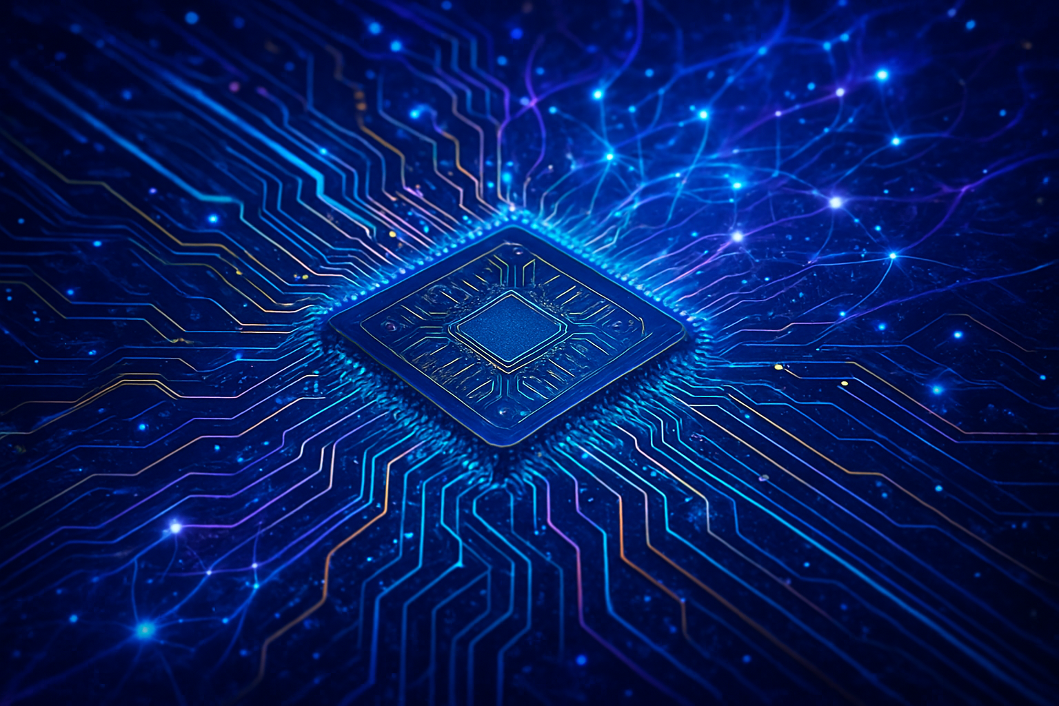
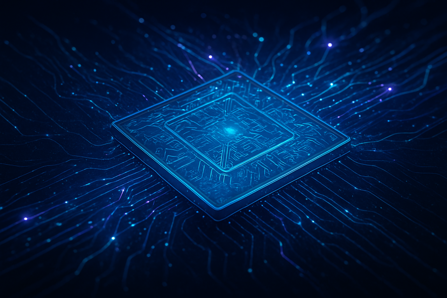
Tag: AI Hardware

  • KLA Corporation Leads the Charge: Process Control Dominance Fuels Bullish Semiconductor Sentiment Amidst AI Boom

    KLA Corporation Leads the Charge: Process Control Dominance Fuels Bullish Semiconductor Sentiment Amidst AI Boom

    The semiconductor industry is experiencing an unprecedented wave of bullish sentiment in 2025, largely propelled by the insatiable demand for Artificial Intelligence (AI) and high-performance computing (HPC). In this dynamic environment, KLA Corporation (NASDAQ: KLAC) has emerged as a standout performer, demonstrating significant outperformance against its peer, Lam Research Corporation (NASDAQ: LRCX). This divergence highlights a critical shift in market confidence, underscoring the escalating importance of precision and quality control in the increasingly complex world of advanced chip manufacturing.

    KLA's leadership signals that while the race to design more powerful AI chips continues, the ability to manufacture them flawlessly and efficiently is becoming an equally, if not more, crucial determinant of success. Investors are keenly observing which companies provide the foundational technologies that enable these cutting-edge innovations, placing a premium on those that can ensure high yields and reliability in an era of miniaturization and sophisticated chip architectures.

    The Technical Edge: KLA's Precision in a Complex World

    KLA Corporation's robust performance is deeply rooted in its market-leading position in process control, defect inspection, and metrology solutions. As of late 2025, KLA commands a dominant market share of approximately 56% in the process control segment, a testament to its indispensable role in modern semiconductor fabrication. With chips becoming denser, featuring advanced packaging techniques, 3D architectures, and ever-shrinking process nodes, the ability to detect and rectify microscopic defects has become paramount for achieving acceptable manufacturing yields. KLA's technologies, particularly its AI-augmented inspection tools and high-bandwidth memory (HBM) process control solutions, are critical enablers for the next generation of AI and HPC applications. The demand for KLA's advanced packaging and process control solutions is projected to surge by a remarkable 70% in 2025, escalating from an estimated $500 million in 2024 to over $850 million.

    In contrast, Lam Research Corporation (NASDAQ: LRCX) remains a powerhouse in deposition and etch equipment, essential processes for building and refining nanometer-scale transistors. In early 2025, Lam introduced its Akara etch system, designed to offer greater precision and speed for advanced 3D memory and logic devices. Its Altus Halo deposition tool is also at the forefront of semiconductor manufacturing innovation. Lam Research was further recognized with the 2025 SEMI Award for North America for its groundbreaking cryogenic etch technology (Lam Cryo™ 3.0), vital for 3D NAND device manufacturing in the AI era, while also offering significant energy and emissions reductions. The company is strategically positioned in Gate-All-Around (GAA) technology and advanced packaging with tools like HALO ALD Moly and SABER 3D.

    The outperformance of KLA, despite Lam Research's significant advancements, highlights a critical differentiation. While Lam Research excels at building the intricate structures of advanced chips, KLA specializes in verifying and optimizing those structures. As manufacturing complexity scales, the need for stringent quality control and defect detection intensifies. The market's current valuation of KLA's niche reflects the industry's focus on mitigating yield losses and ensuring the reliability of increasingly expensive and complex AI chips, making KLA's offerings indispensable at the bleeding edge of semiconductor production. Analyst sentiment further reinforces this, with KLA receiving multiple upgrades and price target increases throughout late 2024 and mid-2025, and Citi maintaining KLA as a "Top Pick" with a $1,060 target in August 2025.

    Competitive Dynamics and Strategic Implications for the AI Ecosystem

    KLA Corporation's (NASDAQ: KLAC) ascendancy in the current market climate has profound implications for the entire AI ecosystem, from chip designers to data center operators. Companies at the forefront of AI chip development, such as NVIDIA Corporation (NASDAQ: NVDA), Advanced Micro Devices, Inc. (NASDAQ: AMD), and Intel Corporation (NASDAQ: INTC), are direct beneficiaries. KLA's sophisticated process control tools enable these firms to achieve higher yields and consistent quality for their highly complex and specialized AI accelerators, critical for performance and cost efficiency. Similarly, major foundries like Taiwan Semiconductor Manufacturing Company Limited (NYSE: TSM) and Samsung Foundry, along with Outsourced Semiconductor Assembly and Test (OSAT) players, heavily rely on KLA's equipment to meet the stringent demands of their advanced manufacturing lines.

    This competitive landscape means that while Lam Research Corporation (NASDAQ: LRCX) remains a crucial partner in chip fabrication, KLA's specialized advantage in process control grants it a unique strategic leverage in a high-growth, high-margin segment. The escalating complexity of AI chips makes robust inspection and metrology capabilities a non-negotiable requirement, effectively solidifying KLA's market positioning as an essential enabler of next-generation technology. For startups and smaller players in the semiconductor equipment space, this trend could lead to increased pressure to innovate rapidly in specialized niches or face consolidation, as larger players like KLA continue to expand their technological leadership.

    The potential disruption lies not in one company replacing another, but in the shifting priorities within the manufacturing workflow. The market's emphasis on KLA underscores that the bottlenecks in advanced chip production are increasingly shifting towards quality assurance and yield optimization. This strategic advantage allows KLA to influence manufacturing roadmaps and standards, ensuring that its tools are integral to any advanced fabrication process, thereby reinforcing its long-term growth trajectory and competitive moats.

    Wider Significance: A Bellwether for AI's Industrialization

    The bullish sentiment in the semiconductor sector, particularly KLA Corporation's (NASDAQ: KLAC) strong performance, serves as a powerful bellwether for the broader industrialization of Artificial Intelligence. This trend signifies that AI is moving beyond theoretical research and initial deployment, demanding robust, scalable, and highly reliable hardware infrastructure. It's no longer just about groundbreaking algorithms; it's equally about the ability to mass-produce the sophisticated silicon that powers them with impeccable precision.

    The impacts of this development are far-reaching. Improved process control and higher manufacturing yields translate directly into more reliable and potentially more affordable AI hardware in the long run, accelerating the adoption of AI across various industries. This efficiency is critical for managing the immense capital expenditures associated with advanced chip fabrication. However, potential concerns include the robustness of the global supply chain, which remains vulnerable to geopolitical tensions and unforeseen disruptions, and the growing talent gap for engineers capable of operating and maintaining such highly specialized and complex equipment. Comparisons to previous AI milestones, such as the initial breakthroughs in deep learning or the rise of large language models, reveal a consistent pattern: advancements in software are always eventually constrained or amplified by the underlying hardware capabilities. KLA's current standing indicates that the industry is now confronting and overcoming these hardware manufacturing hurdles with increasing sophistication.

    This era marks a pivotal moment where manufacturing excellence is as critical as design innovation. The drive for smaller nodes, 3D integration, and heterogeneous computing for AI demands unprecedented levels of control at every stage of production. The market's confidence in KLA reflects a collective understanding that without this foundational precision, the ambitious promises of AI cannot be fully realized, making the semiconductor equipment sector a central pillar in the ongoing AI revolution.

    The Horizon: Future Developments in Precision Manufacturing

    Looking ahead, the trajectory of the semiconductor equipment sector, particularly in process control and metrology, is poised for continued innovation and expansion. Near-term developments will likely focus on further integrating Artificial Intelligence directly into inspection tools, enabling predictive maintenance, real-time anomaly detection, and autonomous process optimization. This self-improving manufacturing ecosystem will be crucial for maintaining high yields as chip designs become even more intricate. In the long term, we can expect advancements that support next-generation computing paradigms, including highly specialized AI accelerators, neuromorphic chips designed to mimic the human brain, and even the foundational hardware for nascent quantum computing technologies.

    Potential applications and use cases on the horizon are vast. Enhanced manufacturing precision will enable the creation of more powerful and energy-efficient edge AI devices, bringing intelligent capabilities closer to the source of data. It will also facilitate the development of more robust autonomous systems, advanced medical diagnostics, and sophisticated scientific research tools that rely on flawless data processing. However, significant challenges remain. The exponential rise in research and development costs for ever-more complex equipment, the daunting task of managing and analyzing petabytes of data generated by billions of inspection points, and ensuring seamless interoperability across diverse vendor equipment are formidable hurdles that need continuous innovation.

    Experts predict a sustained period of strong growth for the process control segment of the semiconductor equipment market, potentially leading to further consolidation as companies seek to acquire specialized expertise and market share. The relentless pursuit of technological boundaries by AI will continue to be the primary catalyst, pushing the semiconductor industry to new heights of precision and efficiency. The coming years will undoubtedly see a fascinating interplay between design ingenuity and manufacturing prowess, with companies like KLA Corporation (NASDAQ: KLAC) playing an instrumental role in shaping the future of AI.

    Comprehensive Wrap-up: Precision as the Pillar of AI's Future

    The current bullish sentiment in the semiconductor sector, epitomized by KLA Corporation's (NASDAQ: KLAC) robust outperformance against Lam Research Corporation (NASDAQ: LRCX), offers critical insights into the evolving landscape of Artificial Intelligence. The key takeaway is the undeniable strategic advantage held by companies specializing in process control, defect inspection, and metrology. As AI chips grow exponentially in complexity, the ability to manufacture them with unparalleled precision and ensure high yields becomes a non-negotiable prerequisite for technological advancement. KLA's dominance in this niche underscores the market's confidence in foundational technologies that directly impact the reliability and scalability of AI hardware.

    This development marks a significant chapter in AI history, emphasizing that the journey to advanced intelligence is as much about the meticulous execution of manufacturing as it is about groundbreaking algorithmic design. The semiconductor sector's health, particularly the performance of its equipment providers, serves as a powerful indicator of the broader tech industry's future trajectory and the sustained momentum of AI innovation. The long-term impact will be a more robust, efficient, and ultimately more accessible AI ecosystem, driven by the foundational quality and precision enabled by companies like KLA.

    In the coming weeks and months, industry watchers should keenly observe quarterly earnings reports from key semiconductor equipment players, paying close attention to guidance on capital expenditures and R&D investments. New product announcements in metrology and inspection, particularly those leveraging AI for enhanced capabilities, will also be crucial indicators. Furthermore, updates on global fab construction and government initiatives aimed at strengthening domestic semiconductor manufacturing will provide additional context for the sustained growth and strategic importance of this vital sector.


    This content is intended for informational purposes only and represents analysis of current AI developments.

    TokenRing AI delivers enterprise-grade solutions for multi-agent AI workflow orchestration, AI-powered development tools, and seamless remote collaboration platforms.
    For more information, visit https://www.tokenring.ai/.

  • India Unleashes Semiconductor Revolution: Rs 1.6 Lakh Crore Investment Ignites Domestic Chip Manufacturing

    India Unleashes Semiconductor Revolution: Rs 1.6 Lakh Crore Investment Ignites Domestic Chip Manufacturing

    New Delhi, India – October 22, 2025 – India has taken a monumental leap towards technological self-reliance with the recent approval of 10 ambitious semiconductor projects, boasting a cumulative investment exceeding Rs 1.6 lakh crore (approximately $18.23 billion). Announced by Union Minister Ashwini Vaishnaw on October 18, 2025, this decisive move under the flagship India Semiconductor Mission (ISM) marks a pivotal moment in the nation's journey to establish a robust, indigenous semiconductor ecosystem. The projects, strategically spread across six states, are poised to drastically reduce India's reliance on foreign chip imports, secure critical supply chains, and position the country as a formidable player in the global semiconductor landscape.

    This massive infusion of capital and strategic focus underscores India's unwavering commitment to becoming a global manufacturing and design hub for electronics. The initiative is expected to catalyze unprecedented economic growth, generate hundreds of thousands of high-skilled jobs, and foster a vibrant ecosystem of innovation, from advanced chip design to cutting-edge manufacturing and packaging. It's a clear signal that India is not just aspiring to be a consumer of technology but a significant producer and innovator, securing its digital future and enhancing its strategic autonomy in an increasingly chip-dependent world.

    A Deep Dive into India's Chipmaking Blueprint: Technical Prowess and Strategic Diversification

    The 10 approved projects represent a diverse and technologically advanced portfolio, meticulously designed to cover various critical aspects of semiconductor manufacturing, from fabrication to advanced packaging. This multi-pronged approach under the India Semiconductor Mission (ISM) aims to build a comprehensive value chain, addressing both current demands and future technological imperatives.

    Among the standout initiatives, SiCSem Private Limited, in collaboration with UK-based Clas-SiC Wafer Fab Ltd., is set to establish India's first commercial Silicon Carbide (SiC) compound semiconductor fabrication facility in Bhubaneswar, Odisha. This is a crucial step as SiC chips are vital for high-power, high-frequency applications found in electric vehicles, 5G infrastructure, and renewable energy systems – sectors where India has significant growth ambitions. Another significant project in Odisha involves 3D Glass Solutions Inc. setting up an advanced packaging and embedded glass substrate facility, focusing on cutting-edge packaging technologies essential for miniaturization and performance enhancement of integrated circuits.

    Further bolstering India's manufacturing capabilities, Continental Device India Private Limited (CDIL) is expanding its Mohali, Punjab plant to produce a wide array of discrete semiconductors including MOSFETs, IGBTs, schottky bypass diodes, and transistors, with an impressive annual capacity of 158.38 million units. This expansion is critical for meeting the burgeoning demand for power management and switching components across various industries. Additionally, Tata Electronics is making substantial strides with an estimated $11 billion fab plant in Gujarat and an OSAT (Outsourced Semiconductor Assembly and Test) facility in Assam, signifying a major entry by an Indian conglomerate into large-scale chip manufacturing and advanced packaging. Not to be overlooked, global giant Micron Technology (NASDAQ: MU) is investing over $2.75 billion in an assembly, testing, marking, and packaging (ATMP) plant, further cementing international confidence in India’s emerging semiconductor ecosystem. These projects collectively represent a departure from previous, more fragmented efforts by providing substantial financial incentives (up to 50% of project costs) and a unified strategic vision, making India a truly attractive destination for high-tech manufacturing. The focus on diverse technologies, from SiC to advanced packaging and traditional silicon-based devices, demonstrates a comprehensive strategy to cater to a wide spectrum of the global chip market.

    Reshaping the AI and Tech Landscape: Corporate Beneficiaries and Competitive Shifts

    The approval of these 10 semiconductor projects under the India Semiconductor Mission is poised to send ripples across the global technology industry, particularly impacting AI companies, tech giants, and startups alike. The immediate beneficiaries are undoubtedly the companies directly involved in the approved projects, such as SiCSem Private Limited, 3D Glass Solutions Inc., Continental Device India Private Limited (CDIL), and Tata Electronics. Their strategic investments are now backed by significant government support, providing a crucial competitive edge in establishing advanced manufacturing capabilities. Micron Technology (NASDAQ: MU), as a global leader, stands to gain from diversified manufacturing locations and access to India's rapidly growing market and talent pool.

    The competitive implications for major AI labs and tech companies are profound. As India develops its indigenous chip manufacturing capabilities, it will reduce the global supply chain vulnerabilities that have plagued the industry in recent years. This will lead to greater stability and potentially lower costs for companies reliant on semiconductors, including those developing AI hardware and running large AI models. Companies like Google (NASDAQ: GOOGL), Microsoft (NASDAQ: MSFT), and Amazon (NASDAQ: AMZN), which are heavily invested in AI infrastructure and cloud computing, could benefit from more reliable and potentially localized chip supplies, reducing their dependence on a concentrated few global foundries. For Indian tech giants and startups, this initiative creates an unprecedented opportunity. Domestic availability of advanced chips and packaging services will accelerate innovation in AI, IoT, automotive electronics, and telecommunications. Startups focused on hardware design and embedded AI solutions will find it easier to prototype, manufacture, and scale their products within India, fostering a new wave of deep tech innovation. This could potentially disrupt existing product development cycles and market entry strategies, as companies with localized manufacturing capabilities gain strategic advantages in terms of cost, speed, and intellectual property protection. The market positioning of companies that invest early and heavily in leveraging India's new semiconductor ecosystem will be significantly enhanced, allowing them to capture a larger share of the burgeoning Indian and global electronics markets.

    A New Era of Geopolitical and Technological Significance

    India's monumental push into semiconductor manufacturing transcends mere economic ambition; it represents a profound strategic realignment within the broader global AI and technology landscape. This initiative positions India as a critical player in the ongoing geopolitical competition for technological supremacy, particularly in an era where chips are the new oil. By building domestic capabilities, India is not only safeguarding its own digital economy but also contributing to the diversification of global supply chains, a crucial concern for nations worldwide after recent disruptions. This move aligns with a global trend of nations seeking greater self-reliance in critical technologies, mirroring efforts in the United States, Europe, and China.

    The impact of this initiative extends to national security, as indigenous chip production reduces vulnerabilities to external pressures and ensures the integrity of vital digital infrastructure. It also signals India's intent to move beyond being just an IT services hub to becoming a hardware manufacturing powerhouse, thereby enhancing its 'Make in India' vision. Potential concerns, however, include the immense capital expenditure required, the need for a highly skilled workforce, and the challenge of competing with established global giants that have decades of experience and massive economies of scale. Comparisons to previous AI milestones, such as the development of large language models or breakthroughs in computer vision, highlight that while AI software innovations are crucial, the underlying hardware infrastructure is equally, if not more, foundational. India's semiconductor mission is a foundational milestone, akin to building the highways upon which future AI innovations will travel, ensuring that the nation has control over its technological destiny rather than being solely dependent on external forces.

    The Road Ahead: Anticipating Future Developments and Addressing Challenges

    The approval of these 10 projects is merely the first major stride in India's long-term semiconductor journey. In the near term, we can expect to see rapid progress in the construction and operationalization of these facilities, with a strong focus on meeting ambitious production timelines. The government's continued financial incentives and policy support will be crucial in overcoming initial hurdles and attracting further investments. Experts predict a significant ramp-up in the domestic production of a range of chips, from power management ICs and discrete components to more advanced logic and memory chips, particularly as the Tata Electronics fab in Gujarat comes online.

    Longer-term developments will likely involve the expansion of these initial projects, the approval of additional fabs, and a deepening of the ecosystem to include upstream (materials, equipment) and downstream (design, software integration) segments. Potential applications and use cases on the horizon are vast, spanning the entire spectrum of the digital economy: smarter automotive systems, advanced telecommunications infrastructure (5G/6G), robust defense electronics, sophisticated AI hardware accelerators, and a new generation of IoT devices. However, significant challenges remain. The immediate need for a highly skilled workforce – from process engineers to experienced fab operators – is paramount. India will need to rapidly scale its educational and vocational training programs to meet this demand. Additionally, ensuring a stable and competitive energy supply, robust water management, and a streamlined regulatory environment will be critical for sustained success. Experts predict that while India's entry will be challenging, its large domestic market, strong engineering talent pool, and geopolitical significance will allow it to carve out a substantial niche, potentially becoming a key alternative supply chain partner in the next decade.

    Charting India's Semiconductor Future: A Concluding Assessment

    India's approval of 10 semiconductor projects worth over Rs 1.6 lakh crore under the India Semiconductor Mission represents a transformative moment in the nation's technological and economic trajectory. The key takeaway is a clear and decisive shift towards self-reliance in a critical industry, moving beyond mere consumption to robust domestic production. This initiative is not just about manufacturing chips; it's about building strategic autonomy, fostering a high-tech ecosystem, and securing India's position in the global digital order.

    This development holds immense significance in AI history as it lays the foundational hardware infrastructure upon which future AI advancements in India will be built. Without a secure and indigenous supply of advanced semiconductors, the growth of AI, IoT, and other emerging technologies would remain vulnerable to external dependencies. The long-term impact is poised to be profound, catalyzing job creation, stimulating exports, attracting further foreign direct investment, and ultimately contributing to India's vision of a $5 trillion economy. As these projects move from approval to implementation, the coming weeks and months will be crucial. We will be watching for progress in facility construction, talent acquisition, and the forging of international partnerships that will further integrate India into the global semiconductor value chain. This initiative is a testament to India's strategic foresight and its determination to become a leading force in the technological innovations of the 21st century.


    This content is intended for informational purposes only and represents analysis of current AI developments.

    TokenRing AI delivers enterprise-grade solutions for multi-agent AI workflow orchestration, AI-powered development tools, and seamless remote collaboration platforms.
    For more information, visit https://www.tokenring.ai/.

  • GSI Technology’s AI Chip Breakthrough Sends Stock Soaring 200% on Cornell Validation

    GSI Technology’s AI Chip Breakthrough Sends Stock Soaring 200% on Cornell Validation

    GSI Technology (NASDAQ: GSIT) experienced an extraordinary surge on Monday, October 20, 2025, as its stock price more than tripled, catapulting the company into the spotlight of the artificial intelligence sector. The monumental leap was triggered by the release of an independent study from Cornell University researchers, which unequivocally validated the groundbreaking capabilities of GSI Technology’s Associative Processing Unit (APU). The study highlighted the Gemini-I APU's ability to deliver GPU-level performance for critical AI workloads, particularly retrieval-augmented generation (RAG) tasks, while consuming a staggering 98% less energy than conventional GPUs. This independent endorsement has sent shockwaves through the tech industry, signaling a potential paradigm shift in energy-efficient AI processing.

    Unpacking the Technical Marvel: Compute-in-Memory Redefines AI Efficiency

    The Cornell University study served as a pivotal moment, offering concrete, third-party verification of GSI Technology’s innovative compute-in-memory architecture. The research specifically focused on the Gemini-I APU, demonstrating its comparable throughput to NVIDIA’s (NASDAQ: NVDA) A6000 GPU for demanding RAG applications. What truly set the Gemini-I apart, however, was its unparalleled energy efficiency. For large datasets, the APU consumed over 98% less power, addressing one of the most pressing challenges in scaling AI infrastructure: energy footprint and operational costs. Furthermore, the Gemini-I APU proved several times faster than standard CPUs in retrieval tasks, slashing total processing time by up to 80% across datasets ranging from 10GB to 200GB.

    This compute-in-memory technology fundamentally differs from traditional Von Neumann architectures, which suffer from the 'memory wall' bottleneck – the constant movement of data between the processor and separate memory modules. GSI's APU integrates processing directly within the memory, enabling massive parallel in-memory computation. This approach drastically reduces data movement, latency, and power consumption, making it ideal for memory-intensive AI inference workloads. While existing technologies like GPUs excel at parallel processing, their high power draw and reliance on external memory interfaces limit their efficiency for certain applications, especially those requiring rapid, large-scale data retrieval and comparison. The initial reactions from the AI research community have been overwhelmingly positive, with many experts hailing the Cornell study as a game-changer that could accelerate the adoption of energy-efficient AI at the edge and in data centers. The validation underscores GSI's long-term vision for a more sustainable and scalable AI future.

    Reshaping the AI Landscape: Impact on Tech Giants and Startups

    The implications of GSI Technology’s (NASDAQ: GSIT) APU breakthrough are far-reaching, poised to reshape competitive dynamics across the AI landscape. While NVIDIA (NASDAQ: NVDA) currently dominates the AI hardware market with its powerful GPUs, GSI's APU directly challenges this stronghold in the crucial inference segment, particularly for memory-intensive workloads like Retrieval-Augmented Generation (RAG). The ability of the Gemini-I APU to match GPU-level throughput with an astounding 98% less energy consumption presents a formidable competitive threat, especially in scenarios where power efficiency and operational costs are paramount. This could compel NVIDIA to accelerate its own research and development into more energy-efficient inference solutions or compute-in-memory technologies to maintain its market leadership.

    Major cloud service providers and AI developers—including Google (NASDAQ: GOOGL), Microsoft (NASDAQ: MSFT), and Amazon (NASDAQ: AMZN) through AWS—stand to benefit immensely from this innovation. These tech giants operate vast data centers that consume prodigious amounts of energy, and the APU offers a crucial pathway to drastically reduce the operational costs and environmental footprint of their AI inference workloads. For Google, the APU’s efficiency in retrieval tasks and its potential to enhance Large Language Models (LLMs) by minimizing hallucinations is highly relevant to its core search and AI initiatives. Similarly, Microsoft and Amazon could leverage the APU to provide more cost-effective and sustainable AI services to their cloud customers, particularly for applications requiring large-scale data retrieval and real-time inference, such as OpenSearch and neural search plugins.

    Beyond the tech giants, the APU’s advantages in speed, efficiency, and programmability position it as a game-changer for Edge AI developers and manufacturers. Companies involved in robotics, autonomous vehicles, drones, and IoT devices will find the APU's low-latency, high-efficiency processing invaluable in power-constrained environments, enabling the deployment of more sophisticated AI at the edge. Furthermore, the defense and aerospace industries, which demand real-time, low-latency AI processing in challenging conditions for applications like satellite imaging and advanced threat detection, are also prime beneficiaries. This breakthrough has the potential to disrupt the estimated $100 billion AI inference market, shifting preferences from general-purpose GPUs towards specialized, power-efficient architectures and intensifying the industry's focus on sustainable AI solutions.

    A New Era of Sustainable AI: Broader Significance and Historical Context

    The wider significance of GSI Technology's (NASDAQ: GSIT) APU breakthrough extends far beyond a simple stock surge; it represents a crucial step in addressing some of the most pressing challenges in modern AI: energy consumption and data transfer bottlenecks. By integrating processing directly within Static Random Access Memory (SRAM), the APU's compute-in-memory architecture fundamentally alters how data is processed. This paradigm shift from traditional Von Neumann architectures, which suffer from the 'memory wall' bottleneck, offers a pathway to more sustainable and scalable AI. The dramatic energy savings—over 98% less power than a GPU for comparable RAG performance—are particularly impactful for enabling widespread Edge AI applications in power-constrained environments like robotics, drones, and IoT devices, and for significantly reducing the carbon footprint of massive data centers.

    This innovation also holds the potential to revolutionize search and generative AI. The APU's ability to rapidly search billions of documents and retrieve relevant information in milliseconds makes it an ideal accelerator for vector search engines, a foundational component of modern Large Language Model (LLM) architectures like ChatGPT. By efficiently providing LLMs with pertinent, domain-specific data, the APU can help minimize hallucinations and deliver more personalized, accurate responses at a lower operational cost. Its impact can be compared to the shift towards GPUs for accelerating deep learning; however, the APU specifically targets extreme power efficiency and data-intensive search/retrieval workloads, addressing the 'AI bottleneck' that even GPUs encounter when data movement becomes the limiting factor. It makes the widespread, low-power deployment of deep learning and Transformer-based models more feasible, especially at the edge.

    However, as with any transformative technology, potential concerns and challenges exist. GSI Technology is a smaller player competing against industry behemoths like NVIDIA (NASDAQ: NVDA) and Intel (NASDAQ: INTC), requiring significant effort to gain widespread market adoption and educate developers. The APU, while exceptionally efficient for specific tasks like RAG and pattern identification, is not a general-purpose processor, meaning its applicability might be narrower and will likely complement, rather than entirely replace, existing AI hardware. Developing a robust software ecosystem and ensuring seamless integration into diverse AI infrastructures are critical hurdles. Furthermore, scaling manufacturing and navigating potential supply chain complexities for specialized SRAM components could pose risks, while the long-term financial performance and investment risks for GSI Technology will depend on its ability to diversify its customer base and demonstrate sustained growth beyond initial validation.

    The Road Ahead: Next-Gen APUs and the Future of AI

    The horizon for GSI Technology's (NASDAQ: GSIT) APU technology is marked by ambitious plans and significant potential, aiming to solidify its position as a disruptive force in AI hardware. In the near term, the company is focused on the rollout and widespread adoption of its Gemini-II APU. This second-generation chip, already in initial testing and being delivered to a key offshore defense contractor for satellite and drone applications, is designed to deliver approximately ten times faster throughput and lower latency than its predecessor, Gemini-I, while maintaining its superior energy efficiency. Built with TSMC's (NYSE: TSM) 16nm process, featuring 6 megabytes of associative memory connected to 100 megabytes of distributed SRAM, the Gemini-II boasts 15 times the memory bandwidth of state-of-the-art parallel processors for AI, with sampling anticipated towards the end of 2024 and market availability in the second half of 2024.

    Looking further ahead, GSI Technology's roadmap includes Plato, a chip targeted at even lower-power edge capabilities, specifically addressing on-device Large Language Model (LLM) applications. The company is also actively developing Gemini-III, slated for release in 2027, which will focus on high-capacity memory and bandwidth applications, particularly for advanced LLMs like GPT-IV. GSI is engaging with hyperscalers to integrate its APU architecture with High Bandwidth Memory (HBM) to tackle critical memory bandwidth, capacity, and power consumption challenges inherent in scaling LLMs. Potential applications are vast and diverse, spanning from advanced Edge AI in robotics and autonomous systems, defense and aerospace for satellite imaging and drone navigation, to revolutionizing vector search and RAG workloads in data centers, and even high-performance computing tasks like drug discovery and cryptography.

    However, several challenges need to be addressed for GSI Technology to fully realize its potential. Beyond the initial Cornell validation, broader independent benchmarks across a wider array of AI workloads and model sizes are crucial for market confidence. The maturity of the APU's software stack and seamless system-level integration into existing AI infrastructure are paramount, as developers need robust tools and clear pathways to utilize this new architecture effectively. GSI also faces the ongoing challenge of market penetration and raising awareness for its compute-in-memory paradigm, competing against entrenched giants. Supply chain complexities and scaling production for specialized SRAM components could also pose risks, while the company's financial performance will depend on its ability to efficiently bring products to market and diversify its customer base. Experts predict a continued shift towards Edge AI, where power efficiency and real-time processing are critical, and a growing industry focus on performance-per-watt, areas where GSI's APU is uniquely positioned to excel, potentially disrupting the AI inference market and enabling a new era of sustainable and ubiquitous AI.

    A Transformative Leap for AI Hardware

    GSI Technology’s (NASDAQ: GSIT) Associative Processing Unit (APU) breakthrough, validated by Cornell University, marks a pivotal moment in the ongoing evolution of artificial intelligence hardware. The core takeaway is the APU’s revolutionary compute-in-memory (CIM) architecture, which has demonstrated GPU-class performance for critical AI inference workloads, particularly Retrieval-Augmented Generation (RAG), while consuming a staggering 98% less energy than conventional GPUs. This unprecedented energy efficiency, coupled with significantly faster retrieval times than CPUs, positions GSI Technology as a potential disruptor in the burgeoning AI inference market.

    In the grand tapestry of AI history, this development represents a crucial evolutionary step, akin to the shift towards GPUs for deep learning, but with a distinct focus on sustainability and efficiency. It directly addresses the escalating energy demands of AI and the 'memory wall' bottleneck that limits traditional architectures. The long-term impact could be transformative: a widespread adoption of APUs could dramatically reduce the carbon footprint of AI operations, democratize high-performance AI by lowering operational costs, and accelerate advancements in specialized fields like Edge AI, defense, aerospace, and high-performance computing where power and latency are critical constraints. This paradigm shift towards processing data directly in memory could pave the way for entirely new computing architectures and methodologies.

    In the coming weeks and months, several key indicators will determine the trajectory of GSI Technology and its APU. Investors and industry observers should closely watch the commercialization efforts for the Gemini-II APU, which promises even greater efficiency and throughput, and the progress of future chips like Plato and Gemini-III. Crucial will be GSI Technology’s ability to scale production, mature its software stack, and secure strategic partnerships and significant customer acquisitions with major players in cloud computing, AI, and defense. While initial financial performance shows revenue growth, the company's ability to achieve consistent profitability will be paramount. Further independent validations across a broader spectrum of AI workloads will also be essential to solidify the APU’s standing against established GPU and CPU architectures, as the industry continues its relentless pursuit of more powerful, efficient, and sustainable AI.


    This content is intended for informational purposes only and represents analysis of current AI developments.

    TokenRing AI delivers enterprise-grade solutions for multi-agent AI workflow orchestration, AI-powered development tools, and seamless remote collaboration platforms.
    For more information, visit https://www.tokenring.ai/.

  • Silicon’s Golden Age: How AI is Propelling the Semiconductor Industry to Unprecedented Heights

    Silicon’s Golden Age: How AI is Propelling the Semiconductor Industry to Unprecedented Heights

    The global semiconductor industry is experiencing an unprecedented surge, positioning itself as a leading sector in current market trading. This remarkable growth is not merely a cyclical upturn but a fundamental shift driven by the relentless advancement and widespread adoption of Artificial Intelligence (AI) and Generative AI (Gen AI). Once heavily reliant on consumer electronics like smartphones and personal computers, the industry's new engine is the insatiable demand for specialized AI data center chips, marking a pivotal transformation in the digital economy.

    This AI-fueled momentum is propelling semiconductor revenues to new stratospheric levels, with projections indicating a global market nearing $800 billion in 2025 and potentially exceeding $1 trillion by 2030. The implications extend far beyond chip manufacturers, touching every facet of the tech industry and signaling a profound reorientation of technological priorities towards computational power tailored for intelligent systems.

    The Microscopic Engines of Intelligence: Decoding AI's Chip Demands

    At the heart of this semiconductor renaissance lies a paradigm shift in computational requirements. Traditional CPUs, while versatile, are increasingly inadequate for the parallel processing demands of modern AI, particularly deep learning and large language models. This has led to an explosive demand for specialized AI chips, such as high-performance Graphics Processing Units (GPUs), Neural Processing Units (NPUs), and Application-Specific Integrated Circuits (ASICs) like Alphabet (NASDAQ: GOOGL) Google's TPUs. These accelerators are meticulously designed to handle the massive datasets and complex calculations inherent in AI and machine learning tasks with unparalleled efficiency.

    The technical specifications of these chips are pushing the boundaries of silicon engineering. High Bandwidth Memory (HBM), for instance, has become a critical supporting technology, offering significantly faster data access compared to conventional DRAM, which is crucial for feeding the hungry AI processors. The memory segment alone is projected to surge by over 24% in 2025, driven by the increasing penetration of high-end products like HBM3 and HBM3e, with HBM4 on the horizon. Furthermore, networking semiconductors are experiencing a projected 13% growth as AI workloads shift the bottleneck from processing to data movement, necessitating advanced chips to overcome latency and throughput challenges within data centers. This specialized hardware differs significantly from previous approaches by integrating dedicated AI acceleration cores, optimized memory interfaces, and advanced packaging technologies to maximize performance per watt, a critical metric for power-intensive AI data centers.

    Initial reactions from the AI research community and industry experts confirm the transformative nature of these developments. Nina Turner, Research Director for Semiconductors at IDC, notes the long-term revenue resilience driven by increased semiconductor content per system and enhanced compute capabilities. Experts from McKinsey & Company (NYSE: MCD) view the surge in generative AI as pushing the industry to innovate faster, approaching a "new S-curve" of technological advancement. The consensus is clear: the semiconductor industry is not just recovering; it's undergoing a fundamental restructuring to meet the demands of an AI-first world.

    Corporate Colossus and Startup Scramble: Navigating the AI Chip Landscape

    The AI-driven semiconductor boom is creating a fierce competitive landscape, significantly impacting tech giants, specialized AI labs, and nimble startups alike. Companies at the forefront of this wave are primarily those designing and manufacturing these advanced chips. NVIDIA Corporation (NASDAQ: NVDA) stands as a monumental beneficiary, dominating the AI accelerator market with its powerful GPUs. Its strategic advantage lies in its CUDA ecosystem, which has become the de facto standard for AI development, making its hardware indispensable for many AI researchers and developers. Other major players like Advanced Micro Devices, Inc. (NASDAQ: AMD) are aggressively expanding their AI chip portfolios, challenging NVIDIA's dominance with their own high-performance offerings.

    Beyond the chip designers, foundries like Taiwan Semiconductor Manufacturing Company Limited (NYSE: TSM), or TSMC, are crucial, as they possess the advanced manufacturing capabilities required to produce these cutting-edge semiconductors. Their technological prowess and capacity are bottlenecks that dictate the pace of AI innovation. The competitive implications are profound: companies that can secure access to advanced fabrication will gain a significant strategic advantage, while those reliant on older technologies risk risking falling behind. This development also fosters a robust ecosystem for startups specializing in niche AI hardware, custom ASICs for specific AI tasks, or innovative cooling solutions for power-hungry AI data centers.

    The market positioning of major cloud providers like Amazon.com, Inc. (NASDAQ: AMZN) with AWS, Microsoft Corporation (NASDAQ: MSFT) with Azure, and Alphabet with Google Cloud is also heavily influenced. These companies are not only massive consumers of AI chips for their cloud infrastructure but are also developing their own custom AI accelerators (e.g., Google's TPUs, Amazon's Inferentia and Trainium) to optimize performance and reduce reliance on external suppliers. This vertical integration strategy aims to disrupt existing products and services by offering highly optimized, cost-effective AI compute. The sheer scale of investment in AI-specific hardware by these tech giants underscores the belief that future competitive advantage will be inextricably linked to superior AI infrastructure.

    A New Industrial Revolution: Broader Implications of the AI Chip Era

    The current surge in the semiconductor industry, driven by AI, fits squarely into the broader narrative of a new industrial revolution. It's not merely an incremental technological improvement but a foundational shift akin to the advent of electricity or the internet. The pervasive impact of AI, from automating complex tasks to enabling entirely new forms of human-computer interaction, hinges critically on the availability of powerful and efficient processing units. This development underscores a significant trend in the AI landscape: the increasing hardware-software co-design, where advancements in algorithms and models are tightly coupled with innovations in chip architecture.

    The impacts are far-reaching. Economically, it's fueling massive investment in R&D, manufacturing infrastructure, and specialized talent, creating new job markets and wealth. Socially, it promises to accelerate the deployment of AI across various sectors, from healthcare and finance to autonomous systems and personalized education, potentially leading to unprecedented productivity gains and new services. However, potential concerns also emerge, including the environmental footprint of energy-intensive AI data centers, the geopolitical implications of concentrated advanced chip manufacturing, and the ethical challenges posed by increasingly powerful AI systems. The US, for instance, has imposed export bans on certain advanced AI chips and manufacturing technologies to China, highlighting the strategic importance and national security implications of semiconductor leadership.

    Comparing this to previous AI milestones, such as the rise of expert systems in the 1980s or the deep learning breakthrough of the 2010s, the current era is distinct due to the sheer scale of computational resources being deployed. While earlier breakthroughs demonstrated AI's potential, the current phase is about operationalizing that potential at a global scale, making AI a ubiquitous utility. The investment in silicon infrastructure reflects a collective bet on AI as the next fundamental layer of technological progress, a bet that dwarfs previous commitments in its ambition and scope.

    The Horizon of Innovation: Future Developments in AI Silicon

    Looking ahead, the trajectory of AI-driven semiconductor innovation promises even more transformative developments. In the near term, experts predict continued advancements in chip architecture, focusing on greater energy efficiency and specialized designs for various AI tasks, from training large models to performing inference at the edge. We can expect to see further integration of AI accelerators directly into general-purpose CPUs and System-on-Chips (SoCs), making AI capabilities more ubiquitous in everyday devices. The ongoing evolution of HBM and other advanced memory technologies will be crucial, as memory bandwidth often becomes the bottleneck for increasingly complex AI models.

    Potential applications and use cases on the horizon are vast. Beyond current applications in cloud computing and autonomous vehicles, future developments could enable truly personalized AI assistants running locally on devices, advanced robotics with real-time decision-making capabilities, and breakthroughs in scientific discovery through accelerated simulations and data analysis. The concept of "Edge AI" will become even more prominent, with specialized, low-power chips enabling sophisticated AI processing directly on sensors, industrial equipment, and smart appliances, reducing latency and enhancing privacy.

    However, significant challenges need to be addressed. The escalating cost of designing and manufacturing cutting-edge chips, the immense power consumption of AI data centers, and the complexities of advanced packaging technologies are formidable hurdles. Geopolitical tensions surrounding semiconductor supply chains also pose a continuous challenge to global collaboration and innovation. Experts predict a future where materials science, quantum computing, and neuromorphic computing will converge with traditional silicon, pushing the boundaries of what's possible. The race for materials beyond silicon, such as carbon nanotubes or 2D materials, could unlock new paradigms for AI hardware.

    A Defining Moment: The Enduring Legacy of AI's Silicon Demand

    In summation, the semiconductor industry's emergence as a leading market sector is unequivocally driven by the surging demand for Artificial Intelligence. The shift from traditional consumer electronics to specialized AI data center chips marks a profound recalibration of the industry's core drivers. This era is characterized by relentless innovation in chip architecture, memory technologies, and networking solutions, all meticulously engineered to power the burgeoning world of AI and generative AI.

    This development holds immense significance in AI history, representing the crucial hardware foundation upon which the next generation of intelligent software will be built. It signifies that AI has moved beyond theoretical research into an era of massive practical deployment, demanding a commensurate leap in computational infrastructure. The long-term impact will be a world increasingly shaped by ubiquitous AI, where intelligent systems are seamlessly integrated into every aspect of daily life and industry, from smart cities to personalized medicine.

    As we move forward, the key takeaways are clear: AI is the primary catalyst, specialized hardware is essential, and the competitive landscape is intensely dynamic. What to watch for in the coming weeks and months includes further announcements from major chip manufacturers regarding next-generation AI accelerators, strategic partnerships between AI developers and foundries, and the ongoing geopolitical maneuvering around semiconductor supply chains. The silicon age, far from waning, is entering its most intelligent and impactful chapter yet, with AI as its guiding force.


    This content is intended for informational purposes only and represents analysis of current AI developments.

    TokenRing AI delivers enterprise-grade solutions for multi-agent AI workflow orchestration, AI-powered development tools, and seamless remote collaboration platforms.
    For more information, visit https://www.tokenring.ai/.

  • Revolutionizing the Chip: Gold Deplating and Wide Bandgap Semiconductors Power AI’s Future

    Revolutionizing the Chip: Gold Deplating and Wide Bandgap Semiconductors Power AI’s Future

    October 20, 2025, marks a pivotal moment in semiconductor manufacturing, where a confluence of groundbreaking new tools and refined processes is propelling chip performance and efficiency to unprecedented levels. At the forefront of this revolution is the accelerated adoption of wide bandgap (WBG) compound semiconductors like Gallium Nitride (GaN) and Silicon Carbide (SiC). These materials are not merely incremental upgrades; they offer superior operating temperatures, higher breakdown voltages, and significantly faster switching speeds—up to ten times quicker than traditional silicon. This leap is critical for meeting the escalating demands of artificial intelligence (AI), high-performance computing (HPC), and electric vehicles (EVs), enabling vastly improved thermal management and drastically lower energy losses. Complementing these material innovations are sophisticated manufacturing techniques, including advanced lithography with High-NA EUV systems and revolutionary packaging solutions like die-to-wafer hybrid bonding and chiplet architectures, which integrate diverse functionalities into single, dense modules.

    Among the critical processes enabling these high-performance chips is the refinement of gold deplating, particularly relevant for the intricate fabrication of wide bandgap compound semiconductors. Gold remains an indispensable material in semiconductor devices due to its exceptional electrical conductivity, resistance to corrosion, and thermal properties, essential for contacts, vias, connectors, and bond pads. Electrolytic gold deplating has emerged as a cost-effective and precise method for "feature isolation"—the removal of the original gold seed layer after electrodeposition. This process offers significant advantages over traditional dry etch methods by producing a smoother gold surface with minimal critical dimension (CD) loss. Furthermore, innovations in gold etchant solutions, such as MacDermid Alpha's non-cyanide MICROFAB AU100 CT DEPLATE, provide precise and uniform gold seed etching on various barriers, optimizing cost efficiency and performance in compound semiconductor fabrication. These advancements in gold processing are crucial for ensuring the reliability and performance of next-generation WBG devices, directly contributing to the development of more powerful and energy-efficient electronic systems.

    The Technical Edge: Precision in a Nanometer World

    The technical advancements in semiconductor manufacturing, particularly concerning WBG compound semiconductors like GaN and SiC, are significantly enhancing efficiency and performance, driven by the insatiable demand for advanced AI and 5G technologies. A key development is the emergence of advanced gold deplating techniques, which offer superior alternatives to traditional methods for critical feature isolation in chip fabrication. These innovations are being met with strong positive reactions from both the AI research community and industry experts, who see them as foundational for the next generation of computing.

    Gold deplating is a process for precisely removing gold from specific areas of a semiconductor wafer, crucial for creating distinct electrical pathways and bond pads. Traditionally, this feature isolation was often performed using expensive dry etch processes in vacuum chambers, which could lead to roughened surfaces and less precise feature definition. In contrast, new electrolytic gold deplating tools, such as the ACM Research (NASDAQ: ACMR) Ultra ECDP and ClassOne Technology's Solstice platform with its proprietary Gen4 ECD reactor, utilize wet processing to achieve extremely uniform removal, minimal critical dimension (CD) loss, and exceptionally smooth gold surfaces. These systems are compatible with various wafer sizes (e.g., 75-200mm, configurable for non-standard sizes up to 200mm) and materials including Silicon, GaAs, GaN on Si, GaN on Sapphire, and Sapphire, supporting applications like microLED bond pads, VCSEL p- and n-contact plating, and gold bumps. The Ultra ECDP specifically targets electrochemical wafer-level gold etching outside the pattern area, ensuring improved uniformity, smaller undercuts, and enhanced gold line appearance. These advancements represent a shift towards more cost-effective and precise manufacturing, as gold is a vital material for its high conductivity, corrosion resistance, and malleability in WBG devices.

    The AI research community and industry experts have largely welcomed these advancements with enthusiasm, recognizing their pivotal role in enabling more powerful and efficient AI systems. Improved semiconductor manufacturing processes, including precise gold deplating, directly facilitate the creation of larger and more capable AI models by allowing for higher transistor density and faster memory access through advanced packaging. This creates a "virtuous cycle," where AI demands more powerful chips, and advanced manufacturing processes, sometimes even aided by AI, deliver them. Companies like Taiwan Semiconductor Manufacturing Company (TSMC) (NYSE: TSM), Intel (NASDAQ: INTC), and Samsung Electronics (KRX: 005930) are at the forefront of adopting these AI-driven innovations for yield optimization, predictive maintenance, and process control. Furthermore, the adoption of gold deplating in WBG compound semiconductors is critical for applications in electric vehicles, 5G/6G communication, RF, and various AI applications, which require superior performance in high-power, high-frequency, and high-temperature environments. The shift away from cyanide-based gold processes towards more environmentally conscious techniques also addresses growing sustainability concerns within the industry.

    Industry Shifts: Who Benefits from the Golden Age of Chips

    The latest advancements in semiconductor manufacturing, particularly focusing on new tools and processes like gold deplating for wide bandgap (WBG) compound semiconductors, are poised to significantly impact AI companies, tech giants, and startups. Gold is a crucial component in advanced semiconductor packaging due to its superior conductivity and corrosion resistance, and its demand is increasing with the rise of AI and premium smartphones. Processes like gold deplating, or electrochemical etching, are essential for precision in manufacturing, enhancing uniformity, minimizing undercuts, and improving the appearance of gold lines in advanced devices. These improvements are critical for wide bandgap semiconductors such as Silicon Carbide (SiC) and Gallium Nitride (GaN), which are vital for high-performance computing, electric vehicles, 5G/6G communication, and AI applications. Companies that successfully implement these AI-driven innovations stand to gain significant strategic advantages, influencing market positioning and potentially disrupting existing product and service offerings.

    AI companies and tech giants, constantly pushing the boundaries of computational power, stand to benefit immensely from these advancements. More efficient manufacturing processes for WBG semiconductors mean faster production of powerful and accessible AI accelerators, GPUs, and specialized processors. This allows companies like NVIDIA (NASDAQ: NVDA), Advanced Micro Devices (NASDAQ: AMD), and Qualcomm (NASDAQ: QCOM) to bring their innovative AI hardware to market more quickly and at a lower cost, fueling the development of even more sophisticated AI models and autonomous systems. Furthermore, AI itself is being integrated into semiconductor manufacturing to optimize design, streamline production, automate defect detection, and refine supply chain management, leading to higher efficiency, reduced costs, and accelerated innovation. Companies like Taiwan Semiconductor Manufacturing Company (TSMC) (NYSE: TSM), Intel (NASDAQ: INTC), and Samsung Electronics (KRX: 005930) are key players in this manufacturing evolution, leveraging AI to enhance their processes and meet the surging demand for AI chips.

    The competitive implications are substantial. Major AI labs and tech companies that can secure access to or develop these advanced manufacturing capabilities will gain a significant edge. The ability to produce more powerful and reliable WBG semiconductors more efficiently can lead to increased market share and strategic advantages. For instance, ACM Research (NASDAQ: ACMR), with its newly launched Ultra ECDP Electrochemical Deplating tool, is positioned as a key innovator in addressing challenges in the growing compound semiconductor market. Technic Inc. and MacDermid are also significant players in supplying high-performance gold plating solutions. Startups, while facing higher barriers to entry due to the capital-intensive nature of advanced semiconductor manufacturing, can still thrive by focusing on specialized niches or developing innovative AI applications that leverage these new, powerful chips. The potential disruption to existing products and services is evident: as WBG semiconductors become more widespread and cost-effective, they will enable entirely new categories of high-performance, energy-efficient AI products and services, potentially rendering older, less efficient silicon-based solutions obsolete in certain applications. This creates a virtuous cycle where advanced manufacturing fuels AI development, which in turn demands even more sophisticated chips.

    Broader Implications: Fueling AI's Exponential Growth

    The latest advancements in semiconductor manufacturing, particularly those focusing on new tools and processes like gold deplating for wide bandgap (WBG) compound semiconductors, are fundamentally reshaping the technological landscape as of October 2025. The insatiable demand for processing power, largely driven by the exponential growth of Artificial Intelligence (AI), is creating a symbiotic relationship where AI both consumes and enables the next generation of chip fabrication. Leading foundries like TSMC (NYSE: TSM) are spearheading massive expansion efforts to meet the escalating needs of AI, with 3nm and emerging 2nm process nodes at the forefront of current manufacturing capabilities. High-NA EUV lithography, capable of patterning features 1.7 times smaller and nearly tripling density, is becoming indispensable for these advanced nodes. Additionally, advancements in 3D stacking and hybrid bonding are allowing for greater integration and performance in smaller footprints. WBG semiconductors, such as GaN and SiC, are proving crucial for high-efficiency power converters, offering superior properties like higher operating temperatures, breakdown voltages, and significantly faster switching speeds—up to ten times quicker than silicon, translating to lower energy losses and improved thermal management for power-hungry AI data centers and electric vehicles.

    Gold deplating, a less conventional but significant process, plays a role in achieving precise feature isolation in semiconductor devices. While dry etch methods are available, electrolytic gold deplating offers a lower-cost alternative with minimal critical dimension (CD) loss and a smoother gold surface, integrating seamlessly with advanced plating tools. This technique is particularly valuable in applications requiring high reliability and performance, such as connectors and switches, where gold's excellent electrical conductivity, corrosion resistance, and thermal conductivity are essential. Gold plating also supports advancements in high-frequency operations and enhanced durability by protecting sensitive components from environmental factors. The ability to precisely control gold deposition and removal through deplating could optimize these connections, especially critical for the enhanced performance characteristics of WBG devices, where gold has historically been used for low inductance electrical connections and to handle high current densities in high-power circuits.

    The significance of these manufacturing advancements for the broader AI landscape is profound. The ability to produce faster, smaller, and more energy-efficient chips is directly fueling AI's exponential growth across diverse fields, including generative AI, edge computing, autonomous systems, and high-performance computing. AI models are becoming more complex and data-hungry, demanding ever-increasing computational power, and advanced semiconductor manufacturing creates a virtuous cycle where more powerful chips enable even more sophisticated AI. This has led to a projected AI chip market exceeding $150 billion in 2025. Compared to previous AI milestones, the current era is marked by AI enabling its own acceleration through more efficient hardware production. While past breakthroughs focused on algorithms and data, the current period emphasizes the crucial role of hardware in running increasingly complex AI models. The impact is far-reaching, enabling more realistic simulations, accelerating drug discovery, and advancing climate modeling. Potential concerns include the increasing cost of developing and manufacturing at advanced nodes, a persistent talent gap in semiconductor manufacturing, and geopolitical tensions that could disrupt supply chains. There are also environmental considerations, as chip manufacturing is highly energy and water intensive, and involves hazardous chemicals, though efforts are being made towards more sustainable practices, including recycling and renewable energy integration.

    The Road Ahead: What's Next for Chip Innovation

    Future developments in advanced semiconductor manufacturing are characterized by a relentless pursuit of higher performance, increased efficiency, and greater integration, particularly driven by the burgeoning demands of artificial intelligence (AI), high-performance computing (HPC), and electric vehicles (EVs). A significant trend is the move towards wide bandgap (WBG) compound semiconductors like Silicon Carbide (SiC) and Gallium Nitride (GaN), which offer superior thermal conductivity, breakdown voltage, and energy efficiency compared to traditional silicon. These materials are revolutionizing power electronics for EVs, renewable energy systems, and 5G/6G infrastructure. To meet these demands, new tools and processes are emerging, such as advanced packaging techniques, including 2.5D and 3D integration, which enable the combination of diverse chiplets into a single, high-density module, thus extending the "More than Moore" era. Furthermore, AI-driven manufacturing processes are becoming crucial for optimizing chip design and production, improving efficiency, and reducing errors in increasingly complex fabrication environments.

    A notable recent development in this landscape is the introduction of specialized tools for gold deplating, particularly for wide bandgap compound semiconductors. As of September 2025, ACM Research (NASDAQ: ACMR) launched its Ultra ECDP (Electrochemical Deplating) tool, specifically designed for wafer-level gold etching in the manufacturing of wide bandgap compound semiconductors like SiC and Gallium Arsenide (GaAs). This tool enhances electrochemical gold etching by improving uniformity, minimizing undercut, and refining the appearance of gold lines, addressing critical challenges associated with gold's use in these advanced devices. Gold is an advantageous material for these devices due to its high conductivity, corrosion resistance, and malleability, despite presenting etching and plating challenges. The Ultra ECDP tool supports processes like gold bump removal and thin film gold etching, integrating advanced features such as cleaning chambers and multi-anode technology for precise control and high surface finish. This innovation is vital for developing high-performance, energy-efficient chips that are essential for next-generation applications.

    Looking ahead, near-term developments (late 2025 into 2026) are expected to see widespread adoption of 2nm and 1.4nm process nodes, driven by Gate-All-Around (GAA) transistors and High-NA EUV lithography, yielding incredibly powerful AI accelerators and CPUs. Advanced packaging will become standard for high-performance chips, integrating diverse functionalities into single modules. Long-term, the semiconductor market is projected to reach a $1 trillion valuation by 2030, fueled by demand from high-performance computing, memory, and AI-driven technologies. Potential applications on the horizon include the accelerated commercialization of neuromorphic chips for embedded AI in IoT devices, smart sensors, and advanced robotics, benefiting from their low power consumption. Challenges that need addressing include the inherent complexity of designing and integrating diverse components in heterogeneous integration, the lack of industry-wide standardization, effective thermal management, and ensuring material compatibility. Additionally, the industry faces persistent talent gaps, supply chain vulnerabilities exacerbated by geopolitical tensions, and the critical need for sustainable manufacturing practices, including efficient gold recovery and recycling from waste. Experts predict continued growth, with a strong emphasis on innovations in materials, advanced packaging, and AI-driven manufacturing to overcome these hurdles and enable the next wave of technological breakthroughs.

    A New Era for AI Hardware: The Golden Standard

    The semiconductor manufacturing landscape is undergoing a rapid transformation driven by an insatiable demand for more powerful, efficient, and specialized chips, particularly for artificial intelligence (AI) applications. As of October 2025, several cutting-edge tools and processes are defining this new era. Extreme Ultraviolet (EUV) lithography continues to advance, enabling the creation of features as small as 7nm and below with fewer steps, boosting resolution and efficiency in wafer fabrication. Beyond traditional scaling, the industry is seeing a significant shift towards "more than Moore" approaches, emphasizing advanced packaging technologies like CoWoS, SoIC, hybrid bonding, and 3D stacking to integrate multiple components into compact, high-performance systems. Innovations such as Gate-All-Around (GAA) transistor designs are entering production, with TSMC (NYSE: TSM) and Intel (NASDAQ: INTC) slated to scale these in 2025, alongside backside power delivery networks that promise reduced heat and enhanced performance. AI itself is becoming an indispensable tool within manufacturing, optimizing quality control, defect detection, process optimization, and even chip design through AI-driven platforms that significantly reduce development cycles and improve wafer yields.

    A particularly noteworthy advancement for wide bandgap compound semiconductors, critical for electric vehicles, 5G/6G communication, RF, and AI applications, is the emergence of advanced gold deplating processes. In September 2025, ACM Research (NASDAQ: ACMR) launched its Ultra ECDP Electrochemical Deplating tool, specifically engineered for electrochemical wafer-level gold (Au) etching in the manufacturing of these specialized semiconductors. Gold, prized for its high conductivity, corrosion resistance, and malleability, presents unique etching and plating challenges. The Ultra ECDP tool tackles these by offering improved uniformity, smaller undercuts, enhanced gold line appearance, and specialized processes for Au bump removal, thin film Au etching, and deep-hole Au deplating. This precision technology is crucial for optimizing devices built on substrates like silicon carbide (SiC) and gallium arsenide (GaAs), ensuring superior electrical conductivity and reliability in increasingly miniaturized and high-performance components. The integration of such precise deplating techniques underscores the industry's commitment to overcoming material-specific challenges to unlock the full potential of advanced materials.

    The significance of these developments in AI history is profound, marking a defining moment where hardware innovation directly dictates the pace and scale of AI progress. These advancements are the fundamental enablers for the ever-increasing computational demands of large language models, advanced computer vision, and sophisticated reinforcement learning, propelling AI into truly ubiquitous applications from hyper-personalized edge devices to entirely new autonomous systems. The long-term impact points towards a global semiconductor market projected to exceed $1 trillion by 2030, potentially reaching $2 trillion by 2040, driven by this symbiotic relationship between AI and semiconductor technology. Key takeaways include the relentless push for miniaturization to sub-2nm nodes, the indispensable role of advanced packaging, and the critical need for energy-efficient designs as power consumption becomes a growing concern. In the coming weeks and months, industry observers should watch for the continued ramp-up of next-generation AI chip production, such as Nvidia's (NASDAQ: NVDA) Blackwell wafers in the US, the further progress of Intel's (NASDAQ: INTC) 18A process, and TSMC's (NYSE: TSM) accelerated capacity expansions driven by strong AI demand. Additionally, developments from emerging players in advanced lithography and the broader adoption of chiplet architectures, especially in demanding sectors like automotive, will be crucial indicators of the industry's trajectory.


    This content is intended for informational purposes only and represents analysis of current AI developments.

    TokenRing AI delivers enterprise-grade solutions for multi-agent AI workflow orchestration, AI-powered development tools, and seamless remote collaboration platforms.
    For more information, visit https://www.tokenring.ai/.

  • Beyond the Silicon Ceiling: Next-Gen AI Chips Ignite a New Era of Intelligence

    Beyond the Silicon Ceiling: Next-Gen AI Chips Ignite a New Era of Intelligence

    The relentless pursuit of artificial general intelligence (AGI) and the explosive growth of large language models (LLMs) are pushing the boundaries of traditional computing, ushering in a transformative era for AI chip architectures. We are witnessing a profound shift beyond the conventional CPU and GPU paradigms, as innovators race to develop specialized, energy-efficient, and brain-inspired silicon designed to unlock unprecedented AI capabilities. This architectural revolution is not merely an incremental upgrade; it represents a foundational re-thinking of how AI processes information, promising to dismantle existing computational bottlenecks and pave the way for a future where intelligent systems are faster, more efficient, and ubiquitous.

    The immediate significance of these next-generation AI chips cannot be overstated. They are the bedrock upon which the next wave of AI innovation will be built, addressing critical challenges such as the escalating energy consumption of AI data centers, the "von Neumann bottleneck" that limits data throughput, and the demand for real-time, on-device AI in countless applications. From neuromorphic processors mimicking the human brain to optical chips harnessing the speed of light, these advancements are poised to accelerate AI development cycles, enable more complex and sophisticated AI models, and ultimately redefine the scope of what artificial intelligence can achieve across industries.

    A Deep Dive into Architectural Revolution: From Neurons to Photons

    The innovations driving next-generation AI chip architectures are diverse and fundamentally depart from the general-purpose designs that have dominated computing for decades. At their core, these new architectures aim to overcome the limitations of the von Neumann architecture—where processing and memory are separate, leading to significant energy and time costs for data movement—and to provide hyper-specialized efficiency for AI workloads.

    Neuromorphic Computing stands out as a brain-inspired paradigm. Chips like Intel's (NASDAQ: INTC) Loihi and IBM's TrueNorth utilize spiking neural networks (SNNs), mimicking biological neurons that communicate via electrical spikes. A key differentiator is their inherent integration of computation and memory, dramatically reducing the von Neumann bottleneck. These chips boast ultra-low power consumption, often operating at 1% to 10% of traditional processors' power draw, and excel in real-time processing, making them ideal for edge AI applications. For instance, Intel's Loihi 2 features 1 million neurons and 128 million synapses, offering significant improvements in energy efficiency and latency for event-driven, sparse AI workloads compared to conventional GPUs.

    In-Memory Computing (IMC) and Analog AI Accelerators represent another significant leap. IMC performs computations directly within or adjacent to memory, drastically cutting down data transfer overhead. This approach is particularly effective for the multiply-accumulate (MAC) operations central to deep learning. Analog AI accelerators often complement IMC by using analog circuits for computations, consuming significantly less energy than their digital counterparts. Innovations like ferroelectric field-effect transistors (FeFET) and phase-change memory are enhancing the efficiency and compactness of IMC solutions. For example, startups like Mythic and Cerebras Systems (private) are developing analog and wafer-scale engines, respectively, to push the boundaries of in-memory and near-memory computation, claiming orders of magnitude improvements in performance-per-watt for specific AI inference tasks. D-Matrix's 3D Digital In-Memory Compute (3DIMC) technology, for example, aims to offer superior speed and energy efficiency compared to traditional High Bandwidth Memory (HBM) for AI inference.

    Optical/Photonic AI Chips are perhaps the most revolutionary, leveraging light (photons) instead of electrons for processing. These chips promise machine learning tasks at the speed of light, potentially classifying wireless signals within nanoseconds—about 100 times faster than the best digital alternatives—while being significantly more energy-efficient and generating less heat. By encoding and processing data with light, photonic chips can perform key deep neural network computations entirely optically on-chip. Lightmatter (private) and Ayar Labs (private) are notable players in this emerging field, developing silicon photonics solutions that could revolutionize applications from 6G wireless systems to autonomous vehicles by enabling ultra-fast, low-latency AI inference directly at the source of data.

    Finally, Domain-Specific Architectures (DSAs), Application-Specific Integrated Circuits (ASICs), and Neural Processing Units (NPUs) represent a broader trend towards "hyper-specialized silicon." Unlike general-purpose CPUs/GPUs, DSAs are meticulously engineered for specific AI workloads, such as large language models, computer vision, or edge inference. Google's (NASDAQ: GOOGL) Tensor Processing Units (TPUs) are a prime example, optimized specifically for AI workloads in data centers, delivering unparalleled performance for tasks like TensorFlow model training. Similarly, Google's Coral NPUs are designed for energy-efficient on-device inference. These custom chips achieve higher performance and energy efficiency by shedding the overhead of general-purpose designs, providing a tailored fit for the unique computational patterns of AI.

    Initial reactions from the AI research community and industry experts are overwhelmingly positive, albeit with a healthy dose of realism regarding the challenges ahead. Many see these architectural shifts as not just necessary but inevitable for AI to continue its exponential growth. Experts highlight the potential for these chips to democratize advanced AI by making it more accessible and affordable, especially for resource-constrained applications. However, concerns remain about the complexity of developing software stacks for these novel architectures and the significant investment required for their commercialization and mass production.

    Industry Impact: Reshaping the AI Competitive Landscape

    The advent of next-generation AI chip architectures is poised to dramatically reshape the competitive landscape for AI companies, tech giants, and startups alike. This shift favors entities capable of deep hardware-software co-design and those willing to invest heavily in specialized silicon.

    NVIDIA (NASDAQ: NVDA), currently the undisputed leader in AI hardware with its dominant GPU accelerators, faces both opportunities and challenges. While NVIDIA continues to innovate with new GPU generations like Blackwell, incorporating features like transformer engines and greater memory bandwidth, the rise of highly specialized architectures could eventually erode its general-purpose AI supremacy for certain workloads. NVIDIA is proactively responding by investing in its own software ecosystem (CUDA) and developing more specialized solutions, but the sheer diversity of new architectures means competition will intensify.

    Tech giants like Google (NASDAQ: GOOGL), Amazon (NASDAQ: AMZN), and Microsoft (NASDAQ: MSFT) are significant beneficiaries, primarily through their massive cloud infrastructure and internal AI development. Google's TPUs have given it a strategic advantage in AI training for its own services and Google Cloud. Amazon's AWS has its own Inferentia and Trainium chips, and Microsoft is reportedly developing its own custom AI silicon. These companies leverage their vast resources to design chips optimized for their specific cloud workloads, reducing reliance on external vendors and gaining performance and cost efficiencies. This vertical integration allows them to offer more competitive AI services to their customers.

    Startups are a vibrant force in this new era, often focusing on niche architectural innovations that established players might overlook or find too risky. Companies like Cerebras Systems (private) with its wafer-scale engine, Mythic (private) with analog in-memory compute, Lightmatter (private) and Ayar Labs (private) with optical computing, and SambaNova Systems (private) with its reconfigurable dataflow architecture, are all aiming to disrupt the market. These startups, often backed by significant venture capital, are pushing the boundaries of what's possible, potentially creating entirely new market segments or offering compelling alternatives for specific AI tasks where traditional GPUs fall short. Their success hinges on demonstrating superior performance-per-watt or unique capabilities for emerging AI paradigms.

    The competitive implications are profound. For major AI labs and tech companies, access to or ownership of cutting-edge AI silicon becomes a critical strategic advantage, influencing everything from research velocity to the cost of deploying large-scale AI services. This could lead to a further consolidation of AI power among those who can afford to design and fabricate their own chips, or it could foster a more diverse ecosystem if specialized startups gain significant traction. Potential disruption to existing products or services is evident, particularly for general-purpose AI acceleration, as specialized chips can offer vastly superior efficiency for their intended tasks. Market positioning will increasingly depend on a company's ability to not only develop advanced AI models but also to run them on the most optimal and cost-effective hardware, making silicon innovation a core competency for any serious AI player.

    Wider Significance: Charting AI's Future Course

    The emergence of next-generation AI chip architectures is not merely a technical footnote; it represents a pivotal moment in the broader AI landscape, profoundly influencing its trajectory and capabilities. This wave of innovation fits squarely into the overarching trend of AI industrialization and specialization, moving beyond theoretical breakthroughs to practical, scalable, and efficient deployment.

    The impacts are multifaceted. Firstly, these chips are instrumental in tackling the "AI energy squeeze." As AI models grow exponentially in size and complexity, their computational demands translate into colossal energy consumption for training and inference. Architectures like neuromorphic, in-memory, and optical computing offer orders of magnitude improvements in energy efficiency, making AI more sustainable and reducing the environmental footprint of massive data centers. This is crucial for the long-term viability and public acceptance of widespread AI deployment.

    Secondly, these advancements are critical for the realization of ubiquitous AI at the edge. The ability to perform complex AI tasks on devices with limited power budgets—smartphones, autonomous vehicles, IoT sensors, wearables—is unlocked by these energy-efficient designs. This will enable real-time, personalized, and privacy-preserving AI applications that don't rely on constant cloud connectivity, fundamentally changing how we interact with technology and our environment. Imagine autonomous drones making split-second decisions with minimal latency or medical wearables providing continuous, intelligent health monitoring.

    However, the wider significance also brings potential concerns. The increasing specialization of hardware could lead to greater vendor lock-in, making it harder for developers to port AI models across different platforms without significant re-optimization. This could stifle innovation if a diverse ecosystem of interoperable hardware and software does not emerge. There are also ethical considerations related to the accelerated capabilities of AI, particularly in areas like autonomous systems and surveillance, where ultra-fast, on-device AI could pose new challenges for oversight and control.

    Comparing this to previous AI milestones, this architectural shift is as significant as the advent of GPUs for deep learning or the development of specialized TPUs. While those were crucial steps, the current wave goes further by fundamentally rethinking the underlying computational model itself, rather than just optimizing existing paradigms. It's a move from brute-force parallelization to intelligent, purpose-built computation, reminiscent of how the human brain evolved highly specialized regions for different tasks. This marks a transition from general-purpose AI acceleration to a truly heterogeneous computing future where the right tool (chip architecture) is matched precisely to the AI task at hand, promising to unlock capabilities that were previously unimaginable due to power or performance constraints.

    The Road Ahead: Future Developments and Expert Predictions

    The trajectory of next-generation AI chip architectures promises a fascinating and rapid evolution in the coming years. In the near term, we can expect a continued refinement and commercialization of the architectures currently under development. This includes more mature software development kits (SDKs) and programming models for neuromorphic and in-memory computing, making them more accessible to a broader range of AI developers. We will likely see a proliferation of specialized ASICs and NPUs for specific large language models (LLMs) and generative AI tasks, offering optimized performance for these increasingly dominant workloads.

    Longer term, experts predict a convergence of these innovative approaches, leading to hybrid architectures that combine the best aspects of different paradigms. Imagine a chip integrating optical interconnects for ultra-fast data transfer, neuromorphic cores for energy-efficient inference, and specialized digital accelerators for high-precision training. This heterogeneous integration, possibly facilitated by advanced chiplet designs and 3D stacking, will unlock unprecedented levels of performance and efficiency.

    Potential applications and use cases on the horizon are vast. Beyond current applications, these chips will be crucial for developing truly autonomous systems that can learn and adapt in real-time with minimal human intervention, from advanced robotics to fully self-driving vehicles operating in complex, unpredictable environments. They will enable personalized, always-on AI companions that deeply understand user context and intent, running sophisticated models directly on personal devices. Furthermore, these architectures are essential for pushing the boundaries of scientific discovery, accelerating simulations in fields like materials science, drug discovery, and climate modeling by handling massive datasets with unparalleled speed.

    However, significant challenges need to be addressed. The primary hurdle remains the software stack. Developing compilers, frameworks, and programming tools that can efficiently map diverse AI models onto these novel, often non-Von Neumann architectures is a monumental task. Manufacturing processes for exotic materials and complex 3D structures also present considerable engineering challenges and costs. Furthermore, the industry needs to establish common benchmarks and standards to accurately compare the performance and efficiency of these vastly different chip designs.

    Experts predict that the next five to ten years will see a dramatic shift in how AI hardware is designed and consumed. The era of a single dominant chip architecture for all AI tasks is rapidly fading. Instead, we are moving towards an ecosystem of highly specialized and interconnected processors, each optimized for specific aspects of the AI workload. The focus will increasingly be on system-level optimization, where the interaction between hardware, software, and the AI model itself is paramount. This will necessitate closer collaboration between chip designers, AI researchers, and application developers to fully harness the potential of these revolutionary architectures.

    A New Dawn for AI: The Enduring Significance of Architectural Innovation

    The emergence of next-generation AI chip architectures marks a pivotal inflection point in the history of artificial intelligence. It is a testament to the relentless human ingenuity in overcoming computational barriers and a clear indicator that the future of AI will be defined as much by hardware innovation as by algorithmic breakthroughs. This architectural revolution, encompassing neuromorphic, in-memory, optical, and domain-specific designs, is fundamentally reshaping the capabilities and accessibility of AI.

    The key takeaways are clear: we are moving towards a future of hyper-specialized, energy-efficient, and data-movement-optimized AI hardware. This shift is not just about making AI faster; it's about making it sustainable, ubiquitous, and capable of tackling problems previously deemed intractable due to computational constraints. The significance of this development in AI history can be compared to the invention of the transistor or the microprocessor—it's a foundational change that will enable entirely new categories of AI applications and accelerate the journey towards more sophisticated and intelligent systems.

    In the long term, these innovations will democratize advanced AI, allowing complex models to run efficiently on everything from massive cloud data centers to tiny edge devices. This will foster an explosion of creativity and application development across industries. The environmental benefits, through drastically reduced power consumption, are also a critical aspect of their enduring impact.

    What to watch for in the coming weeks and months includes further announcements from both established tech giants and innovative startups regarding their next-generation chip designs and strategic partnerships. Pay close attention to the development of robust software ecosystems for these new architectures, as this will be a crucial factor in their widespread adoption. Additionally, observe how benchmarks evolve to accurately measure the unique performance characteristics of these diverse computational paradigms. The race to build the ultimate AI engine is intensifying, and the future of artificial intelligence will undoubtedly be forged in silicon.


    This content is intended for informational purposes only and represents analysis of current AI developments.

    TokenRing AI delivers enterprise-grade solutions for multi-agent AI workflow orchestration, AI-powered development tools, and seamless remote collaboration platforms.
    For more information, visit https://www.tokenring.ai/.

  • The Symbiotic Revolution: How Hardware-Software Co-Design is Unleashing AI’s True Potential

    The Symbiotic Revolution: How Hardware-Software Co-Design is Unleashing AI’s True Potential

    In the rapidly evolving landscape of artificial intelligence, a fundamental shift is underway: the increasingly tight integration of chip hardware and AI software. This symbiotic relationship, often termed hardware-software co-design, is no longer a mere optimization but a critical necessity for unlocking the next generation of AI capabilities. As AI models, particularly large language models (LLMs) and generative AI, grow exponentially in complexity and demand unprecedented computational power, the traditional approach of developing hardware and software in isolation is proving insufficient. The industry is witnessing a holistic embrace of co-design, where silicon and algorithms are crafted in unison, forging a path to unparalleled performance, efficiency, and innovation.

    This integrated approach is immediately significant because it addresses the core bottlenecks that have constrained AI's progress. By tailoring hardware architectures to the specific demands of AI workloads and simultaneously optimizing software to exploit these specialized capabilities, developers are achieving breakthroughs in speed, energy efficiency, and scalability. This synergy is not just about incremental gains; it's about fundamentally redefining what's possible in AI, enabling real-time applications, pushing AI to the edge, and fostering the development of entirely new model architectures that were once deemed computationally intractable. The future of AI is being built on this foundation of deeply intertwined hardware and software.

    The Engineering Behind AI's New Frontier: Unpacking Hardware-Software Co-Design

    The technical essence of hardware-software co-design in AI silicon lies in its departure from the general-purpose computing paradigm. Historically, CPUs and even early GPUs were designed with broad applicability in mind, leading to inefficiencies when confronted with the highly parallel and matrix-multiplication-heavy workloads characteristic of deep learning. The co-design philosophy, however, involves a deliberate, iterative process where hardware architects and AI software engineers collaborate from conception to deployment.

    Specific details of this advancement include the proliferation of specialized AI accelerators like NVIDIA's (NASDAQ: NVDA) GPUs, Google's (NASDAQ: GOOGL) Tensor Processing Units (TPUs), and a growing array of Application-Specific Integrated Circuits (ASICs) and Neural Processing Units (NPUs) from companies like AMD (NASDAQ: AMD), Intel (NASDAQ: INTC), and Apple (NASDAQ: AAPL). These chips feature architectures explicitly designed for AI, incorporating vast numbers of processing cores, optimized memory hierarchies (e.g., High-Bandwidth Memory or HBM), and instruction sets tailored for AI operations. Software stacks, from low-level drivers and compilers to high-level AI frameworks like TensorFlow and PyTorch, are then meticulously optimized to leverage these hardware features. This includes techniques such as low-precision arithmetic (INT8, BF16 quantization), sparsity exploitation, and graph optimization, which are implemented at both hardware and software levels to reduce computational load and memory footprint without significant accuracy loss.

    This approach differs significantly from previous methods where hardware was a fixed target for software optimization. Instead, hardware designers now incorporate insights from AI model architectures and training/inference patterns directly into chip design, while software developers adapt their algorithms to best utilize the unique characteristics of the underlying silicon. For instance, Google's TPUs were designed from the ground up for TensorFlow workloads, offering a tightly coupled hardware-software ecosystem. Similarly, Apple's M-series chips integrate powerful Neural Engines directly onto the SoC, enabling highly efficient on-device AI. Initial reactions from the AI research community and industry experts have been overwhelmingly positive, recognizing this trend as indispensable for sustaining the pace of AI innovation. Researchers are increasingly exploring "hardware-aware" AI model design, where model architectures are developed with the target hardware in mind, leading to more efficient and performant solutions.

    Reshaping the AI Competitive Landscape: Winners, Losers, and Strategic Plays

    The trend of tighter hardware-software integration is profoundly reshaping the competitive landscape across AI companies, tech giants, and startups, creating clear beneficiaries and potential disruptors. Companies that possess both deep expertise in chip design and robust AI software capabilities are poised to dominate this new era.

    NVIDIA (NASDAQ: NVDA) stands out as a prime beneficiary, having pioneered the GPU-accelerated computing paradigm for AI. Its CUDA platform, a tightly integrated software stack with its powerful GPUs, has created a formidable ecosystem that is difficult for competitors to replicate. Google (NASDAQ: GOOGL) with its TPUs and custom AI software stack for its cloud services and internal AI research, is another major player leveraging co-design to its advantage. Apple (NASDAQ: AAPL) has strategically integrated its Neural Engine into its M-series chips, enabling powerful on-device AI capabilities that enhance user experience and differentiate its products. Other chipmakers like AMD (NASDAQ: AMD) and Intel (NASDAQ: INTC) are aggressively investing in their own AI accelerators and software platforms, such as AMD's Vitis AI, to compete in this rapidly expanding market.

    The competitive implications are significant. Major AI labs and tech companies that can design or heavily influence custom AI silicon will gain strategic advantages in terms of performance, cost-efficiency, and differentiation. This could lead to a further consolidation of power among the tech giants with the resources to pursue such vertical integration. Startups in specialized AI hardware or software optimization stand to benefit if they can offer unique solutions that integrate seamlessly into existing ecosystems or carve out niche markets. However, those relying solely on general-purpose hardware or lacking the ability to optimize across the stack may find themselves at a disadvantage. Potential disruption to existing products or services includes the accelerated obsolescence of less optimized AI hardware and a shift towards cloud-based or edge AI solutions powered by highly integrated systems. Market positioning will increasingly hinge on a company's ability to deliver end-to-end optimized AI solutions, from the silicon up to the application layer.

    The Broader Canvas: AI's Evolution Through Integrated Design

    This push for tighter hardware-software integration is not an isolated phenomenon but a central pillar in the broader AI landscape, reflecting a maturing industry focused on efficiency and real-world deployment. It signifies a move beyond theoretical AI breakthroughs to practical, scalable, and sustainable AI solutions.

    The impact extends across various domains. In enterprise AI, optimized silicon and software stacks mean faster data processing, more accurate predictions, and reduced operational costs for tasks like fraud detection, supply chain optimization, and personalized customer experiences. For consumer AI, it enables more powerful on-device capabilities, enhancing privacy by reducing reliance on cloud processing for features like real-time language translation, advanced photography, and intelligent assistants. However, potential concerns include the increasing complexity of the AI development ecosystem, which could raise the barrier to entry for smaller players. Furthermore, the reliance on specialized hardware could lead to vendor lock-in, where companies become dependent on a specific hardware provider's ecosystem. Comparisons to previous AI milestones reveal a consistent pattern: each significant leap in AI capability has been underpinned by advancements in computing power. Just as GPUs enabled the deep learning revolution, co-designed AI silicon is enabling the era of ubiquitous, high-performance AI.

    This trend fits into the broader AI landscape by facilitating the deployment of increasingly complex models, such as multimodal LLMs that seamlessly integrate text, vision, and audio. These models demand unprecedented computational throughput and memory bandwidth, which only a tightly integrated hardware-software approach can efficiently deliver. It also drives the trend towards "AI everywhere," making sophisticated AI capabilities accessible on a wider range of devices, from data centers to edge devices like smartphones and IoT sensors. The emphasis on energy efficiency, a direct outcome of co-design, is crucial for sustainable AI development, especially as the carbon footprint of large AI models becomes a growing concern.

    The Horizon of AI: Anticipating Future Developments

    Looking ahead, the trajectory of hardware-software integration in AI silicon promises a future brimming with innovation, pushing the boundaries of what AI can achieve. The near-term will see continued refinement of existing co-design principles, with a focus on even greater specialization and energy efficiency.

    Expected near-term developments include the widespread adoption of chiplets and modular AI accelerators, allowing for more flexible and scalable custom hardware solutions. We will also see advancements in in-memory computing and near-memory processing, drastically reducing data movement bottlenecks and power consumption. Furthermore, the integration of AI capabilities directly into network infrastructure and storage systems will create "AI-native" computing environments. Long-term, experts predict the emergence of entirely new computing paradigms, potentially moving beyond von Neumann architectures to neuromorphic computing or quantum AI, where hardware is fundamentally designed to mimic biological brains or leverage quantum mechanics for AI tasks. These radical shifts will necessitate even deeper hardware-software co-design.

    Potential applications and use cases on the horizon are vast. Autonomous systems, from self-driving cars to robotic surgery, will achieve new levels of reliability and real-time decision-making thanks to highly optimized edge AI. Personalized medicine will benefit from accelerated genomic analysis and drug discovery. Generative AI will become even more powerful and versatile, enabling hyper-realistic content creation, advanced material design, and sophisticated scientific simulations. However, challenges remain. The complexity of designing and optimizing these integrated systems requires highly specialized talent, and the development cycles can be lengthy and expensive. Standardization across different hardware and software ecosystems is also a significant hurdle. Experts predict that the next wave of AI breakthroughs will increasingly come from those who can master this interdisciplinary art of co-design, leading to a golden age of specialized AI hardware and software ecosystems tailored for specific problems.

    A New Era of AI Efficiency and Innovation

    The escalating trend of tighter integration between chip hardware and AI software marks a pivotal moment in the history of artificial intelligence. It represents a fundamental shift from general-purpose computing to highly specialized, purpose-built AI systems, addressing the insatiable computational demands of modern AI models. This hardware-software co-design paradigm is driving unprecedented gains in performance, energy efficiency, and scalability, making previously theoretical AI applications a tangible reality.

    Key takeaways include the critical role of specialized AI accelerators (GPUs, TPUs, ASICs, NPUs) working in concert with optimized software stacks. This synergy is not just an optimization but a necessity for the advancement of complex AI models like LLMs. Companies like NVIDIA (NASDAQ: NVDA), Google (NASDAQ: GOOGL), and Apple (NASDAQ: AAPL), with their vertically integrated hardware and software capabilities, are leading this charge, reshaping the competitive landscape and setting new benchmarks for AI performance. The wider significance of this development lies in its potential to democratize powerful AI, enabling more robust on-device capabilities, fostering sustainable AI development through energy efficiency, and paving the way for entirely new classes of AI applications across industries.

    The long-term impact of this symbiotic revolution cannot be overstated. It is laying the groundwork for AI that is not only more intelligent but also more efficient, accessible, and adaptable. As we move forward, watch for continued innovation in chiplet technology, in-memory computing, and the emergence of novel computing architectures tailored for AI. The convergence of hardware and software is not merely a trend; it is the future of AI, promising to unlock capabilities that will redefine technology and society in the coming weeks and months.


    This content is intended for informational purposes only and represents analysis of current AI developments.

    TokenRing AI delivers enterprise-grade solutions for multi-agent AI workflow orchestration, AI-powered development tools, and seamless remote collaboration platforms.
    For more information, visit https://www.tokenring.ai/.

  • Broadcom: The Unseen Architect Powering the AI Supercomputing Revolution

    Broadcom: The Unseen Architect Powering the AI Supercomputing Revolution

    In the relentless pursuit of artificial intelligence (AI) breakthroughs, the spotlight often falls on the dazzling capabilities of large language models (LLMs) and the generative wonders they unleash. Yet, beneath the surface of these computational marvels lies a sophisticated hardware backbone, meticulously engineered to sustain their insatiable demands. At the forefront of this critical infrastructure stands Broadcom Inc. (NASDAQ: AVGO), a semiconductor giant that has quietly, yet definitively, positioned itself as the unseen architect powering the AI supercomputing revolution and shaping the very foundation of next-generation AI infrastructure.

    Broadcom's strategic pivot and deep technical expertise in custom silicon (ASICs/XPUs) and high-speed networking solutions are not just incremental improvements; they are foundational shifts that enable the unprecedented scale, speed, and efficiency required by today's most advanced AI models. As of October 2025, Broadcom's influence is more pronounced than ever, underscored by transformative partnerships, including a multi-year strategic collaboration with OpenAI to co-develop and deploy custom AI accelerators. This move signifies a pivotal moment where the insights from frontier AI model development are directly embedded into the hardware, promising to unlock new levels of capability and intelligence for the AI era.

    The Technical Core: Broadcom's Silicon and Networking Prowess

    Broadcom's critical contributions to the AI hardware backbone are primarily rooted in its high-speed networking chips and custom accelerators, which are meticulously engineered to meet the stringent demands of AI workloads.

    At the heart of AI supercomputing, Broadcom's Tomahawk series of Ethernet switches are designed for hyperscale data centers and optimized for AI/ML networking. The Tomahawk 5 (BCM78900 Series), for instance, delivered a groundbreaking 51.2 Terabits per second (Tbps) switching capacity on a single chip, supporting up to 256 x 200GbE ports and built on a power-efficient 5nm monolithic die. It introduced advanced adaptive routing, dynamic load balancing, and end-to-end congestion control tailored for AI/ML workloads. The Tomahawk Ultra (BCM78920 Series) further pushes boundaries with ultra-low latency of 250 nanoseconds at 51.2 Tbps throughput and introduces "in-network collectives" (INC) – specialized hardware that offloads common AI communication patterns (like AllReduce) from processors to the network, improving training efficiency by 7-10%. This innovation aims to transform standard Ethernet into a supercomputing-class fabric, significantly closing the performance gap with specialized fabrics like NVIDIA Corporation's (NASDAQ: NVDA) NVLink. The latest Tomahawk 6 (BCM78910 Series) is a monumental leap, offering 102.4 Tbps of switching capacity in a single chip, implemented in 3nm technology, and supporting AI clusters with over one million XPUs. It unifies scale-up and scale-out Ethernet for massive AI deployments and is compliant with the Ultra Ethernet Consortium (UEC).

    Complementing the Tomahawk series is the Jericho3-AI (BCM88890), a network processor specifically repositioned for AI systems. It boasts 28.8 Tbps of throughput and can interconnect up to 32,000 GPUs, creating high-performance fabrics for AI networks with predictable tail latency. Its features, such as perfect load balancing, congestion-free operation, and Zero-Impact Failover, are crucial for significantly shorter job completion times (JCTs) in AI workloads. Broadcom claims Jericho3-AI can provide at least 10% shorter JCTs compared to alternative networking solutions, making expensive AI accelerators 10% more efficient. This directly challenges proprietary solutions like InfiniBand by offering a high-bandwidth, low-latency, and low-power Ethernet-based alternative.

    Further solidifying Broadcom's networking arsenal is the Thor Ultra 800G AI Ethernet NIC, the industry's first 800G AI Ethernet Network Interface Card. This NIC is designed to interconnect hundreds of thousands of XPUs for trillion-parameter AI workloads. It is fully compliant with the open UEC specification, delivering advanced RDMA innovations like packet-level multipathing, out-of-order packet delivery to XPU memory, and programmable congestion control. Thor Ultra modernizes RDMA for large AI clusters, addressing limitations of traditional RDMA and enabling customers to scale AI workloads with unparalleled performance and efficiency in an open ecosystem. Initial reactions from the AI research community and industry experts highlight Broadcom's role as a formidable competitor to NVIDIA, particularly in offering open, standards-based Ethernet solutions that challenge the proprietary nature of NVLink/NVSwitch and InfiniBand, while delivering superior performance and efficiency for AI workloads.

    Reshaping the AI Industry: Impact on Companies and Competitive Dynamics

    Broadcom's strategic focus on custom AI accelerators and high-speed networking solutions is profoundly reshaping the competitive landscape for AI companies, tech giants, and even startups.

    The most significant beneficiaries are hyperscale cloud providers and major AI labs. Companies like Alphabet (NASDAQ: GOOGL) (Google), Meta Platforms Inc. (NASDAQ: META), ByteDance, Microsoft Corporation (NASDAQ: MSFT), and reportedly Apple Inc. (NASDAQ: AAPL), are leveraging Broadcom's expertise to develop custom AI chips. This allows them to tailor silicon precisely to their specific AI workloads, leading to enhanced performance, greater energy efficiency, and lower operational costs, particularly for inference tasks. For OpenAI, the multi-year partnership with Broadcom to co-develop and deploy 10 gigawatts of custom AI accelerators and Ethernet-based network systems is a strategic move to optimize performance and cost-efficiency by embedding insights from its frontier models directly into the hardware and to diversify its hardware base beyond traditional GPU suppliers.

    This strategy introduces significant competitive implications, particularly for NVIDIA. While NVIDIA remains dominant in general-purpose GPUs for AI training, Broadcom's focus on custom ASICs for inference and its leadership in high-speed networking solutions presents a nuanced challenge. Broadcom's custom ASIC offerings enable hyperscalers to diversify their supply chain and reduce reliance on NVIDIA's CUDA-centric ecosystem, potentially eroding NVIDIA's market share in specific inference workloads and pressuring pricing. Furthermore, Broadcom's Ethernet switching and routing chips, where it holds an 80% market share, are critical for scalable AI infrastructure, even for clusters heavily reliant on NVIDIA GPUs, positioning Broadcom as an indispensable part of the overall AI data center architecture. For Intel Corporation (NASDAQ: INTC) and Advanced Micro Devices, Inc. (NASDAQ: AMD), Broadcom's custom ASICs pose a challenge in areas where their general-purpose CPUs or GPUs might otherwise be used for AI workloads, as Broadcom's ASICs often offer better energy efficiency and performance for specific AI tasks.

    Potential disruptions include a broader shift from general-purpose to specialized hardware, where ASICs gain ground in inference due to superior energy efficiency and latency. This could lead to decreased demand for general-purpose GPUs in pure inference scenarios where custom solutions are more cost-effective. Broadcom's advancements in Ethernet networking are also disrupting older networking technologies that cannot meet the stringent demands of AI workloads. Broadcom's market positioning is strengthened by its leadership in custom silicon, deep relationships with hyperscale cloud providers, and dominance in networking interconnects. Its "open ecosystem" approach, which enables interoperability with various hardware, further enhances its strategic advantage, alongside its significant revenue growth in AI-related projects.

    Broader AI Landscape: Trends, Impacts, and Milestones

    Broadcom's contributions extend beyond mere component supply; they are actively shaping the architectural foundations of next-generation AI infrastructure, deeply influencing the broader AI landscape and current trends.

    Broadcom's role aligns with several key trends, most notably the diversification from NVIDIA's dominance. Many major AI players are actively seeking to reduce their reliance on NVIDIA's general-purpose GPUs and proprietary InfiniBand interconnects. Broadcom provides a viable alternative through its custom silicon development and promotion of open, Ethernet-based networking solutions. This is part of a broader shift towards custom silicon, where leading AI companies and cloud providers design their own specialized AI chips, with Broadcom serving as a critical partner. The company's strong advocacy for open Ethernet standards in AI networking, as evidenced by its involvement in the Ultra Ethernet Consortium, contrasts with proprietary solutions, offering customers more choice and flexibility. These factors are crucial for the unprecedented massive data center expansion driven by the demand for AI compute capacity.

    The overall impacts on the AI industry are significant. Broadcom's emergence as a major supplier intensifies competition and innovation in the AI hardware market, potentially spurring further advancements. Its solutions contribute to substantial cost and efficiency optimization through custom silicon and optimized networking, along with crucial supply chain diversification. By enabling tailored performance for advanced models, Broadcom's hardware allows companies to achieve performance optimizations not possible with off-the-shelf hardware, leading to faster training times and lower inference latency.

    However, potential concerns exist. While Broadcom champions open Ethernet, companies extensively leveraging Broadcom for custom ASIC design might experience a different form of vendor lock-in to Broadcom's specialized design and manufacturing expertise. Some specific AI networking mechanisms, like the "scheduled fabric" in Jericho3-AI, remain proprietary, meaning optimal performance might still require Broadcom's specific implementations. The sheer scale of AI infrastructure build-outs, involving multi-billion dollar and multi-gigawatt commitments, also raises concerns about the sustainability of financing these massive endeavors.

    In comparison to previous AI milestones, the shift towards custom ASICs, enabled by Broadcom, mirrors historical transitions from general-purpose to specialized processors in computing. The recognition and address of networking as a critical bottleneck for scaling AI supercomputers, with Broadcom's innovations in high-bandwidth, low-latency Ethernet solutions, is akin to previous breakthroughs in interconnect technologies that enabled larger, more powerful computing clusters. The deep collaboration between OpenAI (designing accelerators) and Broadcom (developing and deploying them) also signifies a move towards tighter hardware-software co-design, a hallmark of successful technological advancements.

    The Horizon: Future Developments and Expert Predictions

    Looking ahead, Broadcom's trajectory in AI hardware is poised for continued innovation and expansion, with several key developments and expert predictions shaping the future.

    In the near term, the OpenAI partnership remains a significant focus, with initial deployments of custom AI accelerators and networking systems expected in the second half of 2026 and continuing through 2029. This collaboration is expected to embed OpenAI's frontier model insights directly into the hardware. Broadcom will continue its long-standing partnership with Google on its Tensor Processing Unit (TPU) roadmap, with involvement in the upcoming TPU v7. The company's Jericho3-AI and its companion Ramon3 fabric chip are expected to qualify for production within a year, enabling even larger and more efficient AI training supercomputers. The Tomahawk 6 will see broader adoption in AI data centers, supporting over one million accelerator chips. The Thor Ultra 800G AI Ethernet NIC will also become a critical component for interconnecting vast numbers of XPUs. Beyond the data center, Broadcom's Wi-Fi 8 silicon ecosystem is designed for AI-era edge networks, including hardware-accelerated telemetry for AI-driven network optimization at the edge.

    Potential applications and use cases are vast, primarily focused on powering hyperscale AI data centers for large language models and generative AI. Broadcom's custom ASICs are optimized for both AI training and inference, offering superior energy efficiency for specific tasks. The emergence of smaller reasoning models and "chain of thought" reasoning in AI, forming the backbone of agentic AI, presents new opportunities for Broadcom's XPUs in inference-heavy workloads. Furthermore, the expansion of edge AI will see Broadcom's Wi-Fi 8 solutions enabling localized intelligence and real-time inference in various devices and environments, from smart homes to predictive analytics.

    Challenges remain, including persistent competition from NVIDIA, though Broadcom's strategy is more complementary, focusing on custom ASICs and networking. The industry also faces the challenge of diversification and vendor lock-in, with hyperscalers actively seeking multi-vendor solutions. The capital intensity of building new, custom processors means only a few companies can afford bespoke silicon, potentially widening the gap between leading AI firms and smaller players. Experts predict a significant shift to specialized hardware like ASICs for optimized performance and cost control. The network is increasingly recognized as a critical bottleneck in large-scale AI deployments, a challenge Broadcom's advanced networking solutions are designed to address. Analysts also predict that inference silicon demand will grow substantially, potentially becoming the largest driver of AI compute spend, where Broadcom's XPUs are expected to play a key role. Broadcom's CEO, Hock Tan, predicts generative AI could significantly increase technology-related GDP from 30% to 40%, adding an estimated $10 trillion in economic value annually.

    A Comprehensive Wrap-Up: Broadcom's Enduring AI Legacy

    Broadcom's journey into the heart of AI hardware has solidified its position as an indispensable force in the rapidly evolving landscape of AI supercomputing and next-generation AI infrastructure. Its dual focus on custom AI accelerators and high-performance, open-standard networking solutions is not merely supporting the current AI boom but actively shaping its future trajectory.

    Key takeaways highlight Broadcom's strategic brilliance in enabling vertical integration for hyperscale cloud providers, allowing them to craft AI stacks precisely tailored to their unique workloads. This empowers them with optimized performance, reduced costs, and enhanced supply chain security, challenging the traditional reliance on general-purpose GPUs. Furthermore, Broadcom's unwavering commitment to Ethernet as the dominant networking fabric for AI, through innovations like the Tomahawk and Jericho series and the Thor Ultra NIC, is establishing an open, interoperable, and scalable alternative to proprietary interconnects, fostering a broader and more resilient AI ecosystem. By addressing the escalating demands of AI workloads with purpose-built networking and custom silicon, Broadcom is enabling the construction of AI supercomputers capable of handling increasingly complex models and scales.

    The overall significance of these developments in AI history is profound. Broadcom is not just a supplier; it is a critical enabler of the industry's shift towards specialized hardware, fostering competition and diversification that will drive further innovation. Its long-term impact is expected to be enduring, positioning Broadcom as a structural winner in AI infrastructure with robust projections for continued AI revenue growth. The company's deep involvement in building the underlying infrastructure for advanced AI models, particularly through its partnership with OpenAI, positions it as a foundational enabler in the pursuit of artificial general intelligence (AGI).

    In the coming weeks and months, readers should closely watch for further developments in the OpenAI-Broadcom custom AI accelerator racks, especially as initial deployments are expected in the latter half of 2026. Any new custom silicon customers or expansions with existing clients, such as rumored work with Apple, will be crucial indicators of market traction. The industry adoption and real-world performance benchmarks of Broadcom's latest networking innovations, including the Thor Ultra NIC, Tomahawk 6, and Jericho4, in large-scale AI supercomputing environments will also be key. Finally, Broadcom's upcoming earnings calls, particularly the Q4 2025 report expected in December, will provide vital updates on its AI revenue trajectory and future outlook, which analysts predict will continue to surge. Broadcom's strategic focus on enabling custom AI silicon and providing leading-edge Ethernet networking positions it as an indispensable partner in the AI revolution, with its influence on the broader AI hardware landscape only expected to grow.


    This content is intended for informational purposes only and represents analysis of current AI developments.

    TokenRing AI delivers enterprise-grade solutions for multi-agent AI workflow orchestration, AI-powered development tools, and seamless remote collaboration platforms.
    For more information, visit https://www.tokenring.ai/.

  • Geopolitical Fault Lines Reshape Global Chip Landscape: Micron’s China Server Chip Exit Signals Deeper Tech Divide

    Geopolitical Fault Lines Reshape Global Chip Landscape: Micron’s China Server Chip Exit Signals Deeper Tech Divide

    The intricate web of the global semiconductor industry is undergoing a profound re-evaluation as escalating US-China tech tensions compel major chipmakers to recalibrate their market presence. This strategic realignment is particularly evident in the critical server chip sector, where companies like Micron Technology (NASDAQ: MU) are making significant shifts, indicative of a broader fragmentation of the technology ecosystem. The ongoing rivalry, characterized by stringent export controls and retaliatory measures, is not merely impacting trade flows but is fundamentally altering long-term investment strategies and supply chain resilience across the AI and high-tech sectors. As of October 17, 2025, these shifts are not just theoretical but are manifesting in concrete business decisions that will shape the future of global technology leadership.

    This geopolitical tug-of-war is forcing a fundamental rethinking of how advanced technology is developed, manufactured, and distributed. For AI companies, which rely heavily on cutting-edge chips for everything from training large language models to powering inference engines, these market shifts introduce both challenges and opportunities. The re-evaluation by chipmakers signals a move towards more localized or diversified supply chains, potentially leading to increased costs but also fostering domestic innovation in key regions. The implications extend beyond economics, touching upon national security, technological sovereignty, and the pace of AI advancement globally.

    Micron's Strategic Retreat: A Deep Dive into Server DRAM and Geopolitical Impact

    Micron Technology's reported decision to exit the server chip business in mainland China marks a pivotal moment in the ongoing US-China tech rivalry. This strategic shift is a direct consequence of a 2023 Chinese government ban on Micron's products in critical infrastructure, citing "cybersecurity risks"—a move widely interpreted as retaliation for US restrictions on China's semiconductor industry. At the heart of this decision are server DRAM (Dynamic Random-Access Memory) chips, which are essential components for data centers, cloud computing infrastructure, and, crucially, the massive server farms that power AI training and inference.

    Server DRAM differs significantly from consumer-grade memory due to its enhanced reliability, error correction capabilities (ECC – Error-Correcting Code memory), and higher density, designed to operate continuously under heavy loads in enterprise environments. Micron, a leading global producer of these advanced memory solutions, previously held a substantial share of the Chinese server memory market. The ban effectively cut off a significant revenue stream for Micron in a critical sector within China. Their new strategy involves continuing to supply Chinese customers operating data centers outside mainland China and focusing on other segments within China, such as automotive and mobile phone memory, which are less directly impacted by the "critical infrastructure" designation. This represents a stark departure from their previous approach of broad market engagement within China's data center ecosystem. Initial reactions from the tech industry have underscored the severity of the geopolitical pressure, with many experts viewing it as a clear signal that companies must increasingly choose sides or at least bifurcate their operations to navigate the complex regulatory landscapes. This move highlights the increasing difficulty for global chipmakers to operate seamlessly across both major economic blocs without facing significant political and economic repercussions.

    Ripple Effects Across the AI and Tech Landscape

    Micron's strategic shift, alongside similar adjustments by other major players, has profound implications for AI companies, tech giants, and startups alike. Companies like NVIDIA (NASDAQ: NVDA), which designs AI accelerators, and major cloud providers such as Amazon (NASDAQ: AMZN) Web Services, Microsoft (NASDAQ: MSFT) Azure, and Alphabet's (NASDAQ: GOOGL) Google Cloud, all rely heavily on a stable and diverse supply of high-performance memory and processing units. The fragmentation of the chip market introduces supply chain complexities and potential cost increases, which could impact the scaling of AI infrastructure.

    While US-based AI companies might see a push towards more secure, domestically sourced components, potentially benefiting companies like Intel (NASDAQ: INTC) with its renewed foundry efforts, Chinese AI companies face an intensified drive for indigenous solutions. This could accelerate the growth of domestic Chinese memory manufacturers, albeit with potential initial performance gaps compared to global leaders. The competitive landscape for major AI labs is shifting, with access to specific types of advanced chips becoming a strategic advantage or bottleneck. For instance, TSMC (NYSE: TSM) diversifying its manufacturing to the US and Europe aims to mitigate geopolitical risks for its global clientele, including major AI chip designers. Conversely, companies like Qualcomm (NASDAQ: QCOM) and ASML (NASDAQ: ASML), deeply integrated into global supply chains, face ongoing challenges in balancing market access with compliance to various national regulations. This environment fosters a "de-risking" mentality, pushing companies to build redundancy and resilience into their supply chains, potentially at the expense of efficiency, but with the long-term goal of geopolitical insulation.

    Broader Implications for the AI Ecosystem

    The re-evaluation of market presence by chipmakers like Micron is not an isolated event but a critical symptom of a broader trend towards technological decoupling between the US and China. This trend fits into the larger AI landscape by creating distinct regional ecosystems, each striving for self-sufficiency in critical technologies. The impacts are multifaceted: on one hand, it stimulates significant investment in domestic semiconductor manufacturing and R&D in both regions, potentially leading to new innovations and job creation. For instance, the US CHIPS Act and similar initiatives in Europe and Asia are direct responses to these geopolitical pressures, aiming to onshore chip production.

    However, potential concerns abound. The bifurcation of technology standards and supply chains could stifle global collaboration, slow down the pace of innovation, and increase the cost of advanced AI hardware. A world with two distinct, less interoperable tech stacks could lead to inefficiencies and limit the global reach of AI solutions. This situation draws parallels to historical periods of technological competition, such as the Cold War space race, but with the added complexity of deeply intertwined global economies. Unlike previous milestones focused purely on technological breakthroughs, this era is defined by the geopolitical weaponization of technology, where access to advanced chips becomes a tool of national power. The long-term impact on AI development could mean divergent paths for AI ethics, data governance, and application development in different parts of the world, leading to a fragmented global AI landscape.

    The Road Ahead: Navigating a Fragmented Future

    Looking ahead, the near-term will likely see further consolidation of chipmakers' operations within specific geopolitical blocs, with increased emphasis on "friend-shoring" and regional supply chain development. We can expect continued government subsidies and incentives in the US, Europe, Japan, and other allied nations to bolster domestic semiconductor capabilities. This could lead to a surge in new fabrication plants and R&D centers outside of traditional hubs. For AI, this means a potential acceleration in the development of custom AI chips and specialized memory solutions tailored for regional markets, aiming to reduce reliance on external suppliers for critical components.

    In the long term, experts predict a more bifurcated global technology landscape. Challenges will include managing the economic inefficiencies of duplicate supply chains, ensuring interoperability where necessary, and preventing a complete divergence of technological standards. The focus will be on achieving a delicate balance between national security interests and the benefits of global technological collaboration. What experts predict is a sustained period of strategic competition, where innovation in AI will be increasingly tied to geopolitical advantage. Future applications might see AI systems designed with specific regional hardware and software stacks, potentially impacting global data sharing and collaborative AI research. Watch for continued legislative actions, new international alliances around technology, and the emergence of regional champions in critical AI hardware and software sectors.

    Concluding Thoughts: A New Era for AI and Global Tech

    Micron's strategic re-evaluation in China is more than just a corporate decision; it is a potent symbol of the profound transformation sweeping through the global technology industry, driven by escalating US-China tech tensions. This development underscores a fundamental shift from a globally integrated semiconductor supply chain to one increasingly fragmented along geopolitical lines. For the AI sector, this means navigating a new era where access to cutting-edge hardware is not just a technical challenge but a geopolitical one.

    The significance of this development in AI history cannot be overstated. It marks a departure from a purely innovation-driven competition to one heavily influenced by national security and economic sovereignty. While it may foster domestic innovation and resilience in certain regions, it also carries the risk of increased costs, reduced efficiency, and a potential slowdown in the global pace of AI advancement due to duplicated efforts and restricted collaboration. In the coming weeks and months, the tech world will be watching for further strategic adjustments from other major chipmakers, the evolution of national semiconductor policies, and how these shifts ultimately impact the cost, availability, and performance of the advanced chips that fuel the AI revolution. The future of AI will undoubtedly be shaped by these geopolitical currents.


    This content is intended for informational purposes only and represents analysis of current AI developments.

    TokenRing AI delivers enterprise-grade solutions for multi-agent AI workflow orchestration, AI-powered development tools, and seamless remote collaboration platforms.
    For more information, visit https://www.tokenring.ai/.

  • The Dawn of Hyper-Specialized AI: New Chip Architectures Redefine Performance and Efficiency

    The Dawn of Hyper-Specialized AI: New Chip Architectures Redefine Performance and Efficiency

    The artificial intelligence landscape is undergoing a profound transformation, driven by a new generation of AI-specific chip architectures that are dramatically enhancing performance and efficiency. As of October 2025, the industry is witnessing a pivotal shift away from reliance on general-purpose GPUs towards highly specialized processors, meticulously engineered to meet the escalating computational demands of advanced AI models, particularly large language models (LLMs) and generative AI. This hardware renaissance promises to unlock unprecedented capabilities, accelerate AI development, and pave the way for more sophisticated and energy-efficient intelligent systems.

    The immediate significance of these advancements is a substantial boost in both AI performance and efficiency across the board. Faster training and inference speeds, coupled with dramatic improvements in energy consumption, are not merely incremental upgrades; they are foundational changes enabling the next wave of AI innovation. By overcoming memory bottlenecks and tailoring silicon to specific AI workloads, these new architectures are making previously resource-intensive AI applications more accessible and sustainable, marking a critical inflection point in the ongoing AI supercycle.

    Unpacking the Engineering Marvels: A Deep Dive into Next-Gen AI Silicon

    The current wave of AI chip innovation is characterized by a multi-pronged approach, with hyperscalers, established GPU giants, and innovative startups pushing the boundaries of what's possible. These advancements showcase a clear trend towards specialization, high-bandwidth memory integration, and groundbreaking new computing paradigms.

    Hyperscale cloud providers are leading the charge with custom silicon designed for their specific workloads. Google's (NASDAQ: GOOGL) unveiling of Ironwood, its seventh-generation Tensor Processing Unit (TPU), stands out. Designed specifically for inference, Ironwood delivers an astounding 42.5 exaflops of performance, representing a nearly 2x improvement in energy efficiency over its predecessors and an almost 30-fold increase in power efficiency compared to the first Cloud TPU from 2018. It boasts an enhanced SparseCore, a massive 192 GB of High Bandwidth Memory (HBM) per chip (6x that of Trillium), and a dramatically improved HBM bandwidth of 7.37 TB/s. These specifications are crucial for accelerating enterprise AI applications and powering complex models like Gemini 2.5.

    Traditional GPU powerhouses are not standing still. Nvidia's (NASDAQ: NVDA) Blackwell architecture, including the B200 and the upcoming Blackwell Ultra (B300-series) expected in late 2025, is in full production. The Blackwell Ultra promises 20 petaflops and a 1.5x performance increase over the original Blackwell, specifically targeting AI reasoning workloads with 288GB of HBM3e memory. Blackwell itself offers a substantial generational leap over its predecessor, Hopper, being up to 2.5 times faster for training and up to 30 times faster for cluster inference, with 25 times better energy efficiency for certain inference tasks. Looking further ahead, Nvidia's Rubin AI platform, slated for mass production in late 2025 and general availability in early 2026, will feature an entirely new architecture, advanced HBM4 memory, and NVLink 6, further solidifying Nvidia's dominant 86% market share in 2025. Not to be outdone, AMD (NASDAQ: AMD) is rapidly advancing its Instinct MI300X and the upcoming MI350 series GPUs. The MI325X accelerator, with 288GB of HBM3E memory, was generally available in Q4 2024, while the MI350 series, expected in 2025, promises up to a 35x increase in AI inference performance. The MI450 Series AI chips are also set for deployment by Oracle Cloud Infrastructure (NYSE: ORCL) starting in Q3 2026. Intel (NASDAQ: INTC), while canceling its Falcon Shores commercial offering, is focusing on a "system-level solution at rack scale" with its successor, Jaguar Shores. For AI inference, Intel unveiled "Crescent Island" at the 2025 OCP Global Summit, a new data center GPU based on the Xe3P architecture, optimized for performance-per-watt, and featuring 160GB of LPDDR5X memory, ideal for "tokens-as-a-service" providers.

    Beyond traditional architectures, emerging computing paradigms are gaining significant traction. In-Memory Computing (IMC) chips, designed to perform computations directly within memory, are dramatically reducing data movement bottlenecks and power consumption. IBM Research (NYSE: IBM) has showcased scalable hardware with 3D analog in-memory architecture for large models and phase-change memory for compact edge-sized models, demonstrating exceptional throughput and energy efficiency for Mixture of Experts (MoE) models. Neuromorphic computing, inspired by the human brain, utilizes specialized hardware chips with interconnected neurons and synapses, offering ultra-low power consumption (up to 1000x reduction) and real-time learning. Intel's Loihi 2 and IBM's TrueNorth are leading this space, alongside startups like BrainChip (Akida Pulsar, July 2025, 500 times lower energy consumption) and Innatera Nanosystems (Pulsar, May 2025). Chinese researchers also unveiled SpikingBrain 1.0 in October 2025, claiming it to be 100 times faster and more energy-efficient than traditional systems. Photonic AI chips, which use light instead of electrons, promise extremely high bandwidth and low power consumption, with Tsinghua University's Taichi chip (April 2024) claiming 1,000 times more energy-efficiency than Nvidia's H100.

    Reshaping the AI Industry: Competitive Implications and Market Dynamics

    These advancements in AI-specific chip architectures are fundamentally reshaping the competitive landscape for AI companies, tech giants, and startups alike. The drive for specialized silicon is creating both new opportunities and significant challenges, influencing strategic advantages and market positioning.

    Hyperscalers like Google, Amazon (NASDAQ: AMZN), and Microsoft (NASDAQ: MSFT), with their deep pockets and immense AI workloads, stand to benefit significantly from their custom silicon efforts. Google's Ironwood TPU, for instance, provides a tailored, highly optimized solution for its internal AI development and Google Cloud customers, offering a distinct competitive edge in performance and cost-efficiency. This vertical integration allows them to fine-tune hardware and software, delivering superior end-to-end solutions.

    For major AI labs and tech companies, the competitive implications are profound. While Nvidia continues to dominate the AI GPU market, the rise of custom silicon from hyperscalers and the aggressive advancements from AMD pose a growing challenge. Companies that can effectively leverage these new, more efficient architectures will gain a significant advantage in model training times, inference costs, and the ability to deploy larger, more complex AI models. The focus on energy efficiency is also becoming a key differentiator, as the operational costs and environmental impact of AI grow exponentially. This could disrupt existing products or services that rely on older, less efficient hardware, pushing companies to rapidly adopt or develop their own specialized solutions.

    Startups specializing in emerging architectures like neuromorphic, photonic, and in-memory computing are poised for explosive growth. Their ability to deliver ultra-low power consumption and unprecedented efficiency for specific AI tasks opens up new markets, particularly at the edge (IoT, robotics, autonomous vehicles) where power budgets are constrained. The AI ASIC market itself is projected to reach $15 billion in 2025, indicating a strong appetite for specialized solutions. Market positioning will increasingly depend on a company's ability to offer not just raw compute power, but also highly optimized, energy-efficient, and domain-specific solutions that address the nuanced requirements of diverse AI applications.

    The Broader AI Landscape: Impacts, Concerns, and Future Trajectories

    The current evolution in AI-specific chip architectures fits squarely into the broader AI landscape as a critical enabler of the ongoing "AI supercycle." These hardware innovations are not merely making existing AI faster; they are fundamentally expanding the horizons of what AI can achieve, paving the way for the next generation of intelligent systems that are more powerful, pervasive, and sustainable.

    The impacts are wide-ranging. Dramatically faster training times mean AI researchers can iterate on models more rapidly, accelerating breakthroughs. Improved inference efficiency allows for the deployment of sophisticated AI in real-time applications, from autonomous vehicles to personalized medical diagnostics, with lower latency and reduced operational costs. The significant strides in energy efficiency, particularly from neuromorphic and in-memory computing, are crucial for addressing the environmental concerns associated with the burgeoning energy demands of large-scale AI. This "hardware renaissance" is comparable to previous AI milestones, such as the advent of GPU acceleration for deep learning, but with an added layer of specialization that promises even greater gains.

    However, this rapid advancement also brings potential concerns. The high development costs associated with designing and manufacturing cutting-edge chips could further concentrate power among a few large corporations. There's also the potential for hardware fragmentation, where a diverse ecosystem of specialized chips might complicate software development and interoperability. Companies and developers will need to invest heavily in adapting their software stacks to leverage the unique capabilities of these new architectures, posing a challenge for smaller players. Furthermore, the increasing complexity of these chips demands specialized talent in chip design, AI engineering, and systems integration, creating a talent gap that needs to be addressed.

    The Road Ahead: Anticipating What Comes Next

    Looking ahead, the trajectory of AI-specific chip architectures points towards continued innovation and further specialization, with profound implications for future AI applications. Near-term developments will see the refinement and wider adoption of current generation technologies. Nvidia's Rubin platform, AMD's MI350/MI450 series, and Intel's Jaguar Shores will continue to push the boundaries of traditional accelerator performance, while HBM4 memory will become standard, enabling even larger and more complex models.

    In the long term, we can expect the maturation and broader commercialization of emerging paradigms like neuromorphic, photonic, and in-memory computing. As these technologies scale and become more accessible, they will unlock entirely new classes of AI applications, particularly in areas requiring ultra-low power, real-time adaptability, and on-device learning. There will also be a greater integration of AI accelerators directly into CPUs, creating more unified and efficient computing platforms.

    Potential applications on the horizon include highly sophisticated multimodal AI systems that can seamlessly understand and generate information across various modalities (text, image, audio, video), truly autonomous systems capable of complex decision-making in dynamic environments, and ubiquitous edge AI that brings intelligent processing closer to the data source. Experts predict a future where AI is not just faster, but also more pervasive, personalized, and environmentally sustainable, driven by these hardware advancements. The challenges, however, will involve scaling manufacturing to meet demand, ensuring interoperability across diverse hardware ecosystems, and developing robust software frameworks that can fully exploit the unique capabilities of each architecture.

    A New Era of AI Computing: The Enduring Impact

    In summary, the latest advancements in AI-specific chip architectures represent a critical inflection point in the history of artificial intelligence. The shift towards hyper-specialized silicon, ranging from hyperscaler custom TPUs to groundbreaking neuromorphic and photonic chips, is fundamentally redefining the performance, efficiency, and capabilities of AI applications. Key takeaways include the dramatic improvements in training and inference speeds, unprecedented energy efficiency gains, and the strategic importance of overcoming memory bottlenecks through innovations like HBM4 and in-memory computing.

    This development's significance in AI history cannot be overstated; it marks a transition from a general-purpose computing era to one where hardware is meticulously crafted for the unique demands of AI. This specialization is not just about making existing AI faster; it's about enabling previously impossible applications and democratizing access to powerful AI by making it more efficient and sustainable. The long-term impact will be a world where AI is seamlessly integrated into every facet of technology and society, from the cloud to the edge, driving innovation across all industries.

    As we move forward, what to watch for in the coming weeks and months includes the commercial success and widespread adoption of these new architectures, the continued evolution of Nvidia, AMD, and Google's next-generation chips, and the critical development of software ecosystems that can fully harness the power of this diverse and rapidly advancing hardware landscape. The race for AI supremacy will increasingly be fought on the silicon frontier.


    This content is intended for informational purposes only and represents analysis of current AI developments.

    TokenRing AI delivers enterprise-grade solutions for multi-agent AI workflow orchestration, AI-powered development tools, and seamless remote collaboration platforms.
    For more information, visit https://www.tokenring.ai/.