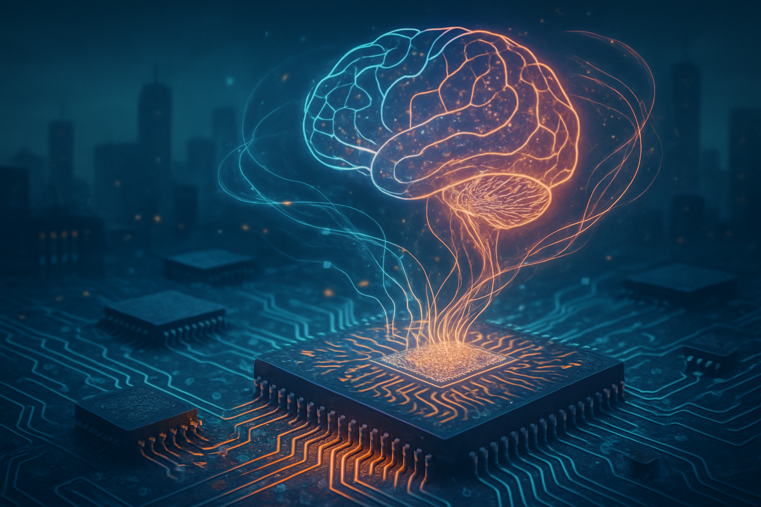
October 27, 2025 – In a groundbreaking stride towards overcoming the inherent energy inefficiencies of modern electronics, scientists are rapidly advancing the field of topological insulators (TIs). These exotic materials, once a theoretical curiosity, are now poised to revolutionize computing and power delivery by creating "electron superhighways"—pathways where electricity flows with unprecedented efficiency and minimal energy loss. This development promises to usher in an era of ultra-low-power devices, faster processors, and potentially unlock new frontiers in quantum computing.
The immediate significance of topological insulators lies in their ability to dramatically reduce heat generation and energy consumption, two critical bottlenecks in the relentless pursuit of more powerful and compact electronics. As silicon-based technologies approach their fundamental limits, TIs offer a fundamentally new paradigm for electron transport, moving beyond traditional conductors that waste significant energy as heat. This shift could redefine the capabilities of everything from personal devices to massive data centers, addressing one of the most pressing challenges facing the tech industry today.
Unpacking the Quantum Mechanics of Dissipationless Flow
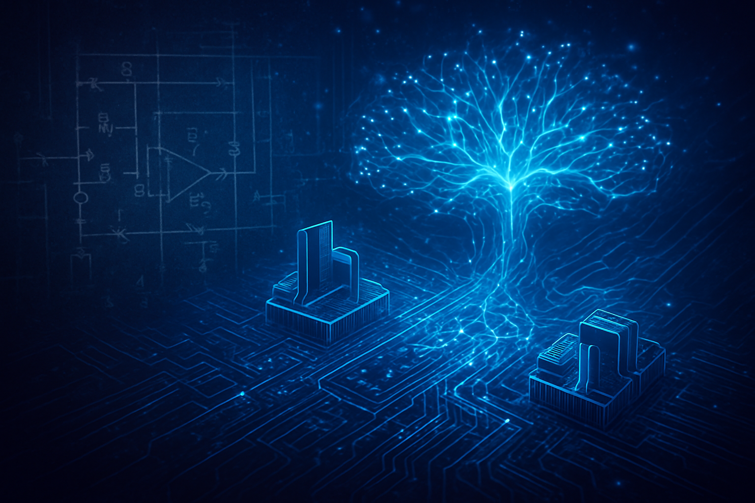
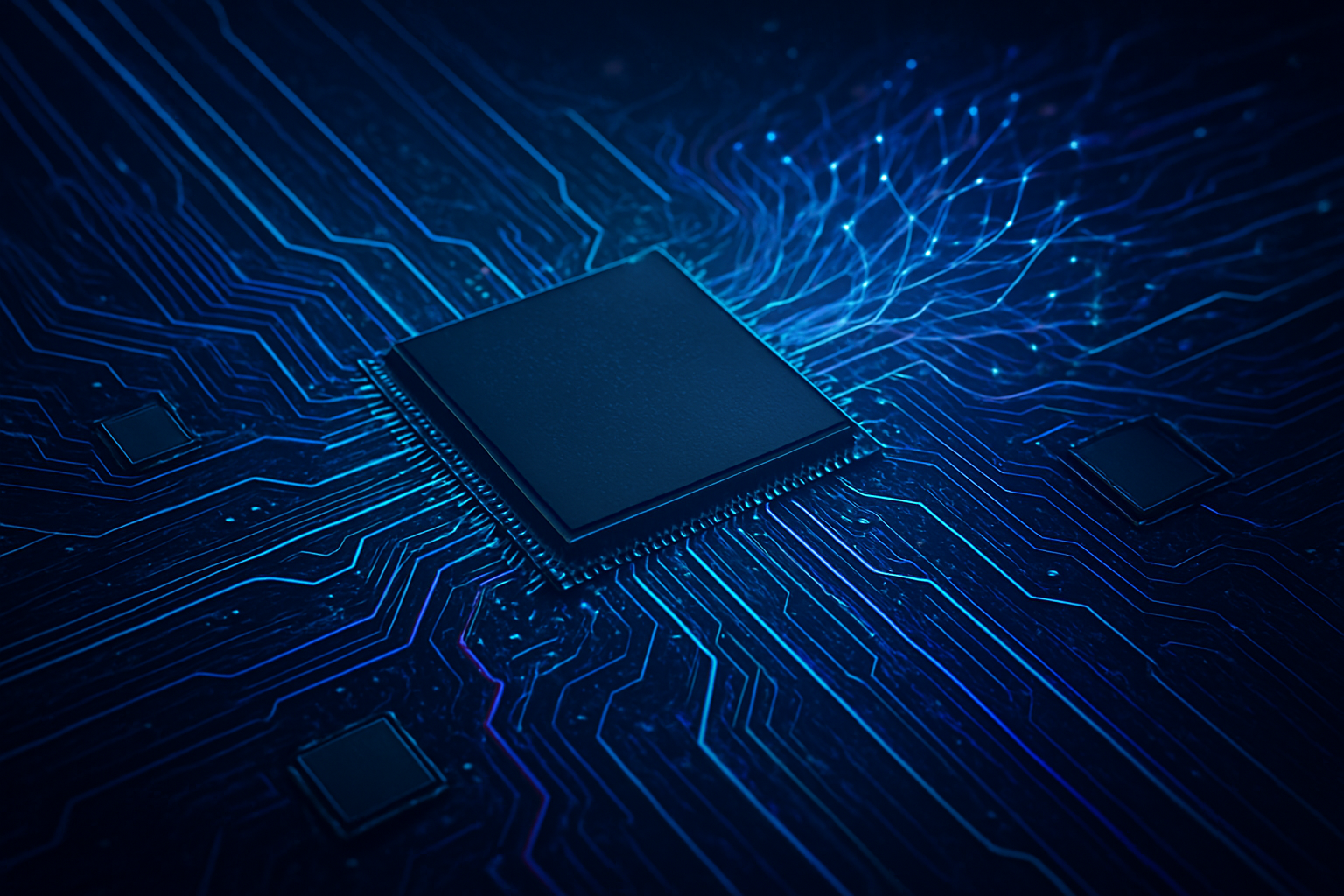
Topological insulators are a unique class of quantum materials that behave as electrical insulators in their bulk interior, much like glass, but astonishingly conduct electricity with near-perfect efficiency along their surfaces or edges. This duality arises from a complex interplay of quantum mechanical principles, notably strong spin-orbit coupling and time-reversal symmetry, which imbue them with a "non-trivial" electronic band structure. Unlike conventional conductors where electrons scatter off impurities and lattice vibrations, generating heat, the surface states of TIs are "topologically protected." This means that defects, imperfections, and non-magnetic impurities have little to no effect on the electron flow, creating the fabled "electron superhighways."
A key feature contributing to this efficient conduction is "spin-momentum locking," where an electron's spin direction is inextricably linked and perpendicular to its direction of motion. This phenomenon effectively suppresses "backscattering"—the primary cause of resistance in traditional materials. For an electron to reverse its direction, its spin would also need to flip, an event that is strongly inhibited in time-reversal symmetric TIs. This "no U-turn" rule ensures that electrons travel largely unimpeded, leading to dissipationless transport. Recent advancements have even demonstrated the creation of multi-layered topological insulators exhibiting the Quantum Anomalous Hall (QAH) effect with higher Chern numbers, essentially constructing multiple parallel superhighways for electrons, significantly boosting information transfer capacity. For example, studies have achieved Chern numbers up to 5, creating 10 effective lanes for electron flow.
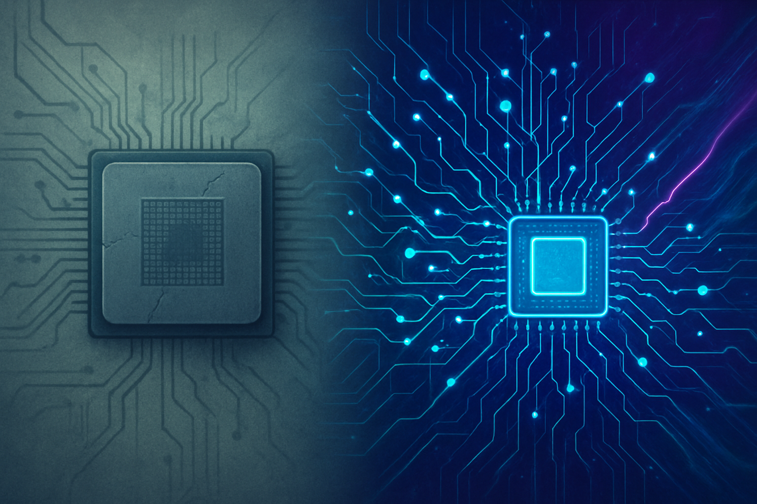
This approach stands in stark contrast to existing technologies, where even the best conductors, like copper, suffer from significant energy loss due to electron scattering. Silicon, the workhorse of modern computing, relies on manipulating charge carriers within a semiconductor, a process that inherently generates heat and requires substantial power. Topological insulators bypass these limitations by leveraging quantum protection, offering a path to fundamentally cooler and more energy-efficient electronic components. The scientific community has met the advancements in TIs with immense excitement, hailing them as a "newly discovered state of quantum matter" and a "groundbreaking discovery" with the potential to "revolutionize electronics." The theoretical underpinnings of topological phases of matter were even recognized with the Nobel Prize in Physics in 2016, underscoring the profound importance of this field.
Strategic Implications for Tech Giants and Innovators
The advent of practical topological insulator technology carries profound implications for a wide array of companies, from established tech giants to agile startups. Companies heavily invested in semiconductor manufacturing, such as Intel (NASDAQ: INTC), Taiwan Semiconductor Manufacturing Company (NYSE: TSM), and Samsung Electronics (KRX: 005930), stand to benefit immensely from incorporating these materials into next-generation chip designs. The ability to create processors that consume less power while operating at higher speeds could provide a significant competitive edge, extending Moore's Law well into the future.
Beyond chip manufacturing, companies focused on data center infrastructure, like Amazon (NASDAQ: AMZN) Web Services, Microsoft (NASDAQ: MSFT) Azure, and Google (NASDAQ: GOOGL) Cloud, could see massive reductions in their energy footprints and cooling costs. The energy savings from dissipationless electron transport could translate into billions of dollars annually, making their cloud services more sustainable and profitable. Furthermore, the development of ultra-low-power components could disrupt the mobile device market, leading to smartphones and wearables with significantly longer battery lives and enhanced performance, benefiting companies like Apple (NASDAQ: AAPL) and Qualcomm (NASDAQ: QCOM).
Startups specializing in novel materials, quantum computing hardware, and spintronics are also uniquely positioned to capitalize on this development. The robust nature of topologically protected states makes them ideal candidates for building fault-tolerant qubits, a holy grail for quantum computing. Companies like IBM (NYSE: IBM) and Google, which are heavily investing in quantum research, could leverage TIs to overcome some of the most persistent challenges in qubit stability and coherence. The market positioning for early adopters of TI technology will be defined by their ability to integrate these complex materials into scalable and manufacturable solutions, potentially creating new industry leaders and reshaping the competitive landscape of the entire electronics sector.
Broader Significance in the AI and Tech Landscape
The emergence of topological insulators fits perfectly into the broader trend of seeking fundamental material science breakthroughs to fuel the next generation of artificial intelligence and high-performance computing. As AI models grow exponentially in complexity and demand ever-increasing computational resources, the energy cost of training and running these models becomes a significant concern. TIs offer a pathway to drastically reduce this energy consumption, making advanced AI more sustainable and accessible. This aligns with the industry's push for "green AI" and more efficient computing architectures.
The impacts extend beyond mere efficiency. The unique spin-momentum locking properties of TIs make them ideal for spintronics, a field that aims to utilize the electron's spin, in addition to its charge, for data storage and processing. This could lead to a new class of memory and logic devices that are not only faster but also non-volatile, retaining data even when power is off. This represents a significant leap from current charge-based electronics and could enable entirely new computing paradigms. Concerns, however, revolve around the scalability of manufacturing these exotic materials, maintaining their topological properties under various environmental conditions, and integrating them seamlessly with existing silicon infrastructure. While recent breakthroughs in higher-temperature operation and silicon compatibility are promising, mass production remains a significant hurdle.
Comparing this to previous AI milestones, the development of TIs is akin to the foundational advancements in semiconductor physics that enabled the integrated circuit. It's not an AI algorithm itself, but a fundamental hardware innovation that will underpin and accelerate future AI breakthroughs. Just as the transistor revolutionized electronics, topological insulators have the potential to spark a similar revolution in how information is processed and stored, providing the physical substrate for a quantum leap in computational power and efficiency that will directly benefit AI development.
The Horizon: Future Developments and Applications
The near-term future of topological insulators will likely focus on refining synthesis techniques, exploring new material compositions, and integrating them into experimental device prototypes. Researchers are particularly keen on pushing the operational temperatures higher, with recent successes demonstrating topological properties at significantly less extreme temperatures (around -213 degrees Celsius) and even room temperature in specific bismuth iodide crystals. The August 2024 discovery of a one-dimensional topological insulator using tellurium further expands the design space, potentially leading to novel applications in quantum wires and qubits.
Long-term developments include the realization of commercial-scale spintronic devices, ultra-low-power transistors, and robust, fault-tolerant qubits for quantum computers. Experts predict that within the next decade, we could see the first commercial products leveraging TI principles, starting perhaps with specialized memory chips or highly efficient sensors. The potential applications are vast, ranging from next-generation solar cells with enhanced efficiency to novel quantum communication devices.
However, significant challenges remain. Scaling up production from laboratory samples to industrial quantities, ensuring material purity, and developing cost-effective manufacturing processes are paramount. Furthermore, integrating these quantum materials with existing classical electronic components requires overcoming complex engineering hurdles. Experts predict continued intense research in academic and industrial labs, focusing on material science, device physics, and quantum engineering. The goal is to move beyond proof-of-concept demonstrations to practical, deployable technologies that can withstand real-world conditions.
A New Foundation for the Digital Age
The advancements in topological insulators mark a pivotal moment in materials science, promising to lay a new foundation for the digital age. By enabling "electron superhighways," these materials offer a compelling solution to the escalating energy demands of modern electronics and the physical limitations of current silicon technology. The ability to conduct electricity with minimal dissipation is not merely an incremental improvement but a fundamental shift that could unlock unprecedented levels of efficiency and performance across the entire computing spectrum.
This development's significance in the broader history of technology cannot be overstated. It represents a paradigm shift from optimizing existing materials to discovering and harnessing entirely new quantum states of matter for technological benefit. The implications for AI, quantum computing, and sustainable electronics are profound, promising a future where computational power is no longer constrained by the heat and energy waste of traditional conductors. As researchers continue to push the boundaries of what's possible with these remarkable materials, the coming weeks and months will be crucial for observing breakthroughs in manufacturing scalability, higher-temperature operation, and the first functional prototypes that demonstrate their transformative potential outside the lab. The race is on to build the next generation of electronics, and topological insulators are leading the charge.
This content is intended for informational purposes only and represents analysis of current AI developments.
TokenRing AI delivers enterprise-grade solutions for multi-agent AI workflow orchestration, AI-powered development tools, and seamless remote collaboration platforms.
For more information, visit https://www.tokenring.ai/.