Lam Research Corporation (NASDAQ: LRCX) has kicked off its fiscal year 2026 with a powerful first quarter, reporting earnings that significantly surpassed analyst expectations. Announced on October 22, 2025, these strong results not only signal a healthy and expanding semiconductor equipment market but also underscore the company's indispensable role in powering the global artificial intelligence (AI) revolution. As a critical enabler of advanced chip manufacturing, Lam Research's performance serves as a key indicator of the sustained capital expenditures by chipmakers scrambling to meet the insatiable demand for AI-specific hardware.
The company's impressive financial showing, particularly its robust revenue and earnings per share, highlights the ongoing technological advancements required for next-generation AI processors and memory. With AI workloads demanding increasingly complex and efficient semiconductors, Lam Research's leadership in critical etch and deposition technologies positions it at the forefront of this transformative era. Its Q1 success is a testament to the surging investments in AI-driven semiconductor manufacturing inflections, making it a crucial bellwether for the entire industry's trajectory in the age of artificial intelligence.
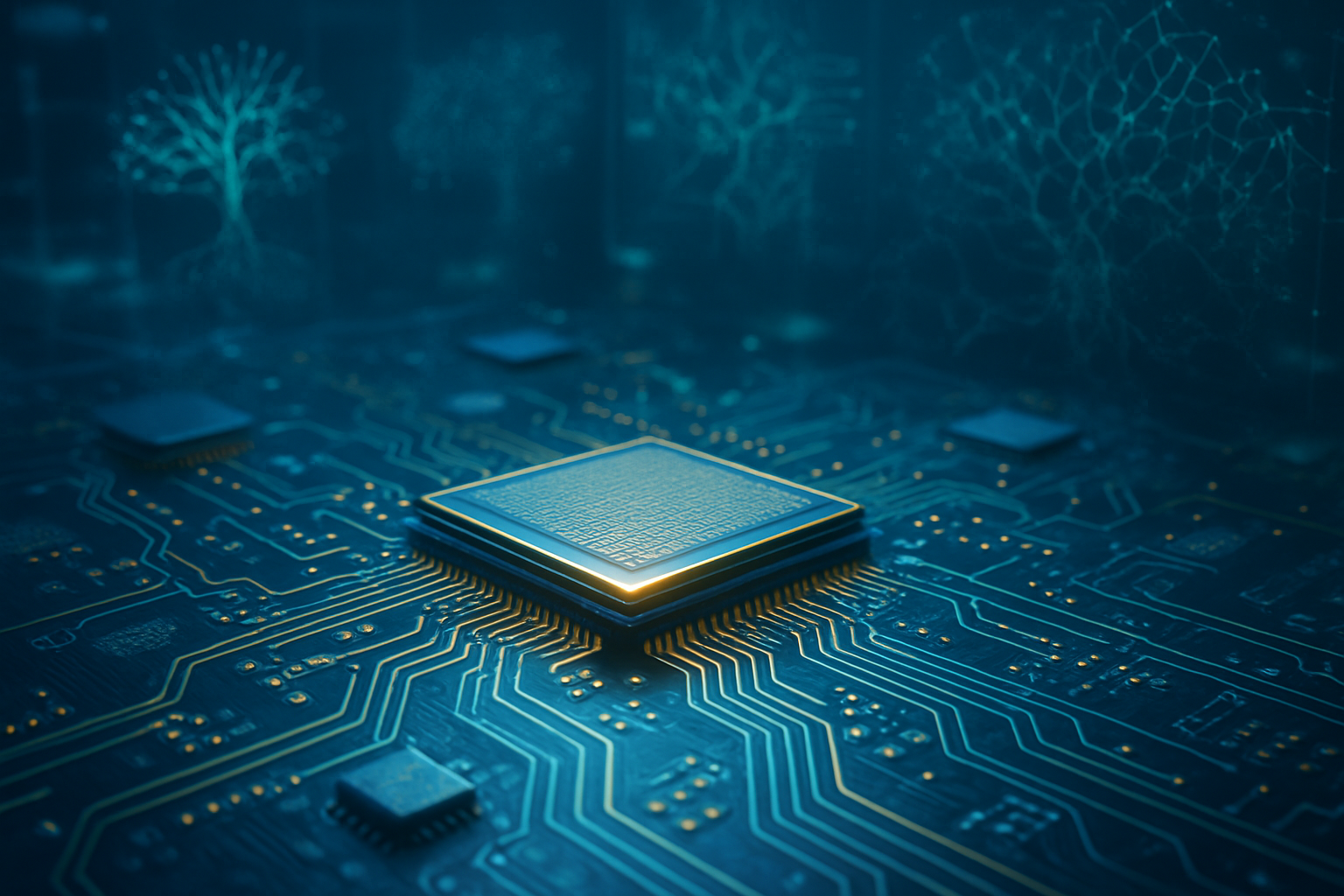
Technical Prowess Driving AI Innovation
Lam Research's stellar Q1 fiscal year 2026 performance, ending September 28, 2025, was marked by several key financial achievements. The company reported revenue of $5.32 billion, comfortably exceeding the consensus analyst forecast of $5.22 billion. U.S. GAAP EPS soared to $1.24, significantly outperforming the $1.21 per share analyst consensus and representing a remarkable increase of over 40% compared to the prior year's Q1. This financial strength is directly tied to Lam Research's advanced technological offerings, which are proving crucial for the intricate demands of AI chip production.
A significant driver of this growth is Lam Research's expertise in advanced packaging and High Bandwidth Memory (HBM) technologies. The re-acceleration of memory investment, particularly for HBM, is vital for high-performance AI accelerators. Lam Research's advanced packaging solutions, such as its SABRE 3D systems, are critical for creating the 2.5D and 3D packages essential for these powerful AI devices, leading to substantial market share gains. These solutions allow for the vertical stacking of memory and logic, drastically reducing data transfer latency and increasing bandwidth—a non-negotiable requirement for efficient AI processing.
Furthermore, Lam Research's tools are fundamental enablers of leading-edge logic nodes and emerging architectures like gate-all-around (GAA) transistors. AI workloads demand processors that are not only powerful but also energy-efficient, pushing the boundaries of semiconductor design. The company's deposition and etch equipment are indispensable for manufacturing these complex, next-generation semiconductor device architectures, which feature increasingly smaller and more intricate structures. Lam Research's innovation in this area ensures that chipmakers can continue to scale performance while managing power consumption, a critical balance for AI at the edge and in the data center.
The introduction of new technologies further solidifies Lam Research's technical leadership. The company recently unveiled VECTOR® TEOS 3D, an inter-die gapfill tool specifically designed to address critical advanced packaging challenges in 3D integration and chiplet technologies. This innovation explicitly paves the way for new AI-accelerating architectures by enabling denser and more reliable interconnections between stacked dies. Such advancements differentiate Lam Research from previous approaches by providing solutions tailored to the unique complexities of 3D heterogeneous integration, an area where traditional 2D scaling methods are reaching their physical limits. Initial reactions from the AI research community and industry experts have been overwhelmingly positive, recognizing these tools as essential for the continued evolution of AI hardware.
Competitive Implications and Market Positioning in the AI Era
Lam Research's robust Q1 performance and its strategic focus on AI-enabling technologies carry significant competitive implications across the semiconductor and AI landscapes. Companies positioned to benefit most directly are the leading-edge chip manufacturers (fabs) like Taiwan Semiconductor Manufacturing Company (TSMC: TPE) and Samsung Electronics (KRX: 005930), as well as memory giants such as SK Hynix (KRX: 000660) and Micron Technology (NASDAQ: MU). These companies rely heavily on Lam Research's advanced equipment to produce the complex logic and HBM chips that power AI servers and devices. Lam's success directly translates to their ability to ramp up production of high-demand AI components.
The competitive landscape for major AI labs and tech companies, including NVIDIA (NASDAQ: NVDA), Google (NASDAQ: GOOGL), Microsoft (NASDAQ: MSFT), and Amazon (NASDAQ: AMZN), is also profoundly affected. As these tech giants invest billions in developing their own AI accelerators and data center infrastructure, the availability of cutting-edge manufacturing equipment becomes a bottleneck. Lam Research's ability to deliver advanced etch and deposition tools ensures that the supply chain for AI chips remains robust, enabling these companies to rapidly deploy new AI models and services. Its leadership in advanced packaging, for instance, is crucial for companies leveraging chiplet architectures to build more powerful and modular AI processors.
Potential disruption to existing products or services could arise if competitors in the semiconductor equipment space, such as Applied Materials (NASDAQ: AMAT) or Tokyo Electron (TYO: 8035), fail to keep pace with Lam Research's innovations in AI-specific manufacturing processes. While the market is large enough for multiple players, Lam's specialized tools for HBM and advanced logic nodes give it a strategic advantage in the highest-growth segments driven by AI. Its focus on solving the intricate challenges of 3D integration and new materials for AI chips positions it as a preferred partner for chipmakers pushing the boundaries of performance.
From a market positioning standpoint, Lam Research has solidified its role as a "critical enabler" and a "quiet supplier" in the AI chip boom. Its strategic advantage lies in providing the foundational equipment that allows chipmakers to produce the smaller, more complex, and higher-performance integrated circuits necessary for AI. This deep integration into the manufacturing process gives Lam Research significant leverage and ensures its sustained relevance as the AI industry continues its rapid expansion. The company's proactive approach to developing solutions for future AI architectures, such as GAA and advanced packaging, reinforces its long-term strategic advantage.
Wider Significance in the AI Landscape
Lam Research's strong Q1 performance is not merely a financial success story; it's a profound indicator of the broader trends shaping the AI landscape. This development fits squarely into the ongoing narrative of AI's insatiable demand for computational power, pushing the limits of semiconductor technology. It underscores that the advancements in AI are inextricably linked to breakthroughs in hardware manufacturing, particularly in areas like advanced packaging, 3D integration, and novel transistor architectures. Lam's results confirm that the industry is in a capital-intensive phase, with significant investments flowing into the foundational infrastructure required to support increasingly complex AI models and applications.
The impacts of this robust performance are far-reaching. It signifies a healthy supply chain for AI chips, which is critical for mitigating potential bottlenecks in AI development and deployment. A strong semiconductor equipment market, led by companies like Lam Research, ensures that the innovation pipeline for AI hardware remains robust, enabling the continuous evolution of machine learning models and the expansion of AI into new domains. Furthermore, it highlights the importance of materials science and precision engineering in achieving AI milestones, moving beyond just algorithmic breakthroughs to encompass the physical realization of intelligent systems.
Potential concerns, however, also exist. The heavy reliance on a few key equipment suppliers like Lam Research could pose risks if there are disruptions in their operations or if geopolitical tensions affect global supply chains. While the current outlook is positive, any significant slowdown in capital expenditure by chipmakers or shifts in technology roadmaps could impact future performance. Moreover, the increasing complexity of manufacturing processes, while enabling advanced AI, also raises the barrier to entry for new players, potentially concentrating power among established semiconductor giants and their equipment partners.
Comparing this to previous AI milestones, Lam Research's current trajectory echoes the foundational role played by hardware innovators during earlier tech booms. Just as specialized hardware enabled the rise of personal computing and the internet, advanced semiconductor manufacturing is now the bedrock for the AI era. This moment can be likened to the early days of GPU acceleration, where NVIDIA's (NASDAQ: NVDA) hardware became indispensable for deep learning. Lam Research, as a "quiet supplier," is playing a similar, albeit less visible, foundational role, enabling the next generation of AI breakthroughs by providing the tools to build the chips themselves. It signifies a transition from theoretical AI advancements to widespread, practical implementation, underpinned by sophisticated manufacturing capabilities.
Future Developments and Expert Predictions
Looking ahead, Lam Research's strong Q1 performance and its strategic focus on AI-enabling technologies portend several key near-term and long-term developments in the semiconductor and AI industries. In the near term, we can expect continued robust capital expenditure from chip manufacturers, particularly those focusing on AI accelerators and high-performance memory. This will likely translate into sustained demand for Lam Research's advanced etch and deposition systems, especially those critical for HBM production and leading-edge logic nodes like GAA. The company's guidance for Q2 fiscal year 2026, while showing a modest near-term contraction in gross margins, still reflects strong revenue expectations, indicating ongoing market strength.
Longer-term, the trajectory of AI hardware will necessitate even greater innovation in materials science and 3D integration. Experts predict a continued shift towards heterogeneous integration, where different types of chips (logic, memory, specialized AI accelerators) are integrated into a single package, often in 3D stacks. This trend will drive demand for Lam Research's advanced packaging solutions, including its SABRE 3D systems and new tools like VECTOR® TEOS 3D, which are designed to address the complexities of inter-die gapfill and robust interconnections. We can also anticipate further developments in novel memory technologies beyond HBM, and advanced transistor architectures that push the boundaries of physics, all requiring new generations of fabrication equipment.
Potential applications and use cases on the horizon are vast, ranging from more powerful and efficient AI in data centers, enabling larger and more complex large language models, to advanced AI at the edge for autonomous vehicles, robotics, and smart infrastructure. These applications will demand chips with higher performance-per-watt, lower latency, and greater integration density, directly aligning with Lam Research's areas of expertise. The company's innovations are paving the way for AI systems that can process information faster, learn more efficiently, and operate with greater autonomy.
However, several challenges need to be addressed. Scaling manufacturing processes to atomic levels becomes increasingly difficult and expensive, requiring significant R&D investments. Geopolitical factors, trade policies, and intellectual property disputes could also impact global supply chains and market access. Furthermore, the industry faces the challenge of attracting and retaining skilled talent capable of working with these highly advanced technologies. Experts predict that the semiconductor equipment market will continue to be a high-growth sector, but success will hinge on continuous innovation, strategic partnerships, and the ability to navigate complex global dynamics. The next wave of AI breakthroughs will be as much about materials and manufacturing as it is about algorithms.
A Crucial Enabler in the AI Revolution's Ascent
Lam Research's strong Q1 fiscal year 2026 performance serves as a powerful testament to its pivotal role in the ongoing artificial intelligence revolution. The key takeaways from this report are clear: the demand for advanced semiconductors, fueled by AI, is not only robust but accelerating, driving significant capital expenditures across the industry. Lam Research, with its leadership in critical etch and deposition technologies and its strategic focus on advanced packaging and HBM, is exceptionally well-positioned to capitalize on and enable this growth. Its financial success is a direct reflection of its technological prowess in facilitating the creation of the next generation of AI-accelerating hardware.
This development's significance in AI history cannot be overstated. It underscores that the seemingly abstract advancements in machine learning and large language models are fundamentally dependent on the tangible, physical infrastructure provided by companies like Lam Research. Without the sophisticated tools to manufacture ever-more powerful and efficient chips, the progress of AI would inevitably stagnate. Lam Research's innovations are not just incremental improvements; they are foundational enablers that unlock new possibilities for AI, pushing the boundaries of what intelligent systems can achieve.
Looking towards the long-term impact, Lam Research's continued success ensures a healthy and innovative semiconductor ecosystem, which is vital for sustained AI progress. Its focus on solving the complex manufacturing challenges of 3D integration and leading-edge logic nodes guarantees that the hardware necessary for future AI breakthroughs will continue to evolve. This positions the company as a long-term strategic partner for the entire AI industry, from chip designers to cloud providers and AI research labs.
In the coming weeks and months, industry watchers should keenly observe several indicators. Firstly, the capital expenditure plans of major chipmakers will provide further insights into the sustained demand for equipment. Secondly, any new technological announcements from Lam Research or its competitors regarding advanced packaging or novel transistor architectures will signal the next frontiers in AI hardware. Finally, the broader economic environment and geopolitical stability will continue to influence the global semiconductor supply chain, impacting the pace and scale of AI infrastructure development. Lam Research's performance remains a critical barometer for the health and future direction of the AI-powered tech industry.
This content is intended for informational purposes only and represents analysis of current AI developments.
TokenRing AI delivers enterprise-grade solutions for multi-agent AI workflow orchestration, AI-powered development tools, and seamless remote collaboration platforms.
For more information, visit https://www.tokenring.ai/.