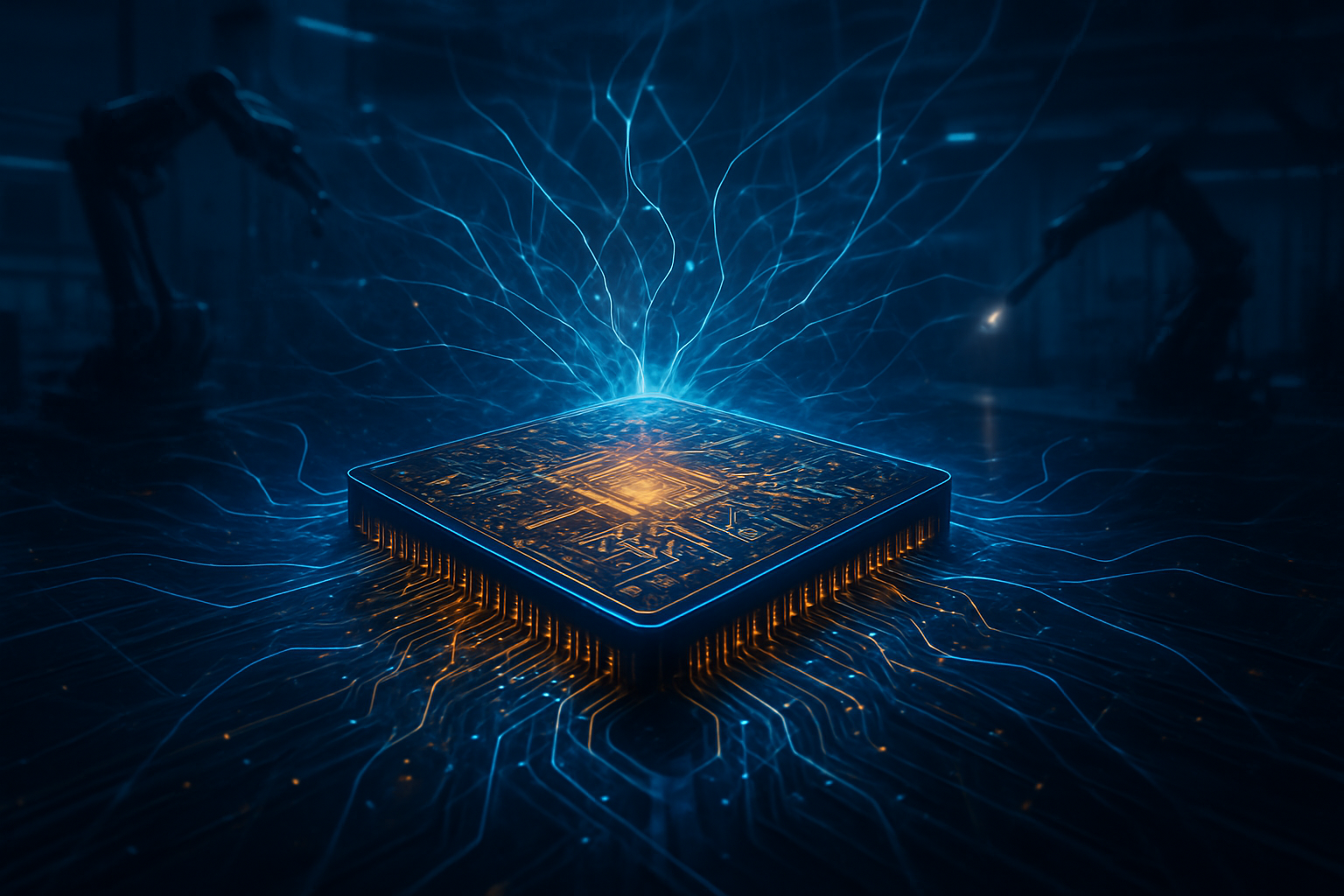
As of January 30, 2026, the global semiconductor landscape has officially entered the "Angstrom Era." Taiwan Semiconductor Manufacturing Company (NYSE: TSM), the world's largest contract chipmaker, has successfully transitioned its 2nm (N2) process from pilot lines to high-volume manufacturing (HVM). This milestone represents more than just a reduction in feature size; it marks the most significant architectural overhaul in semiconductor design since the introduction of FinFET over a decade ago.
The immediate significance of the N2 node cannot be overstated, particularly for the burgeoning artificial intelligence sector. With production now scaling at TSMC's Baoshan and Kaohsiung facilities, the first wave of 2nm-powered devices is expected to hit the market by the end of the year. This shift provides the critical hardware foundation required to sustain the massive compute demands of next-generation large language models and autonomous systems, effectively extending the lifespan of Moore’s Law through sheer architectural ingenuity.
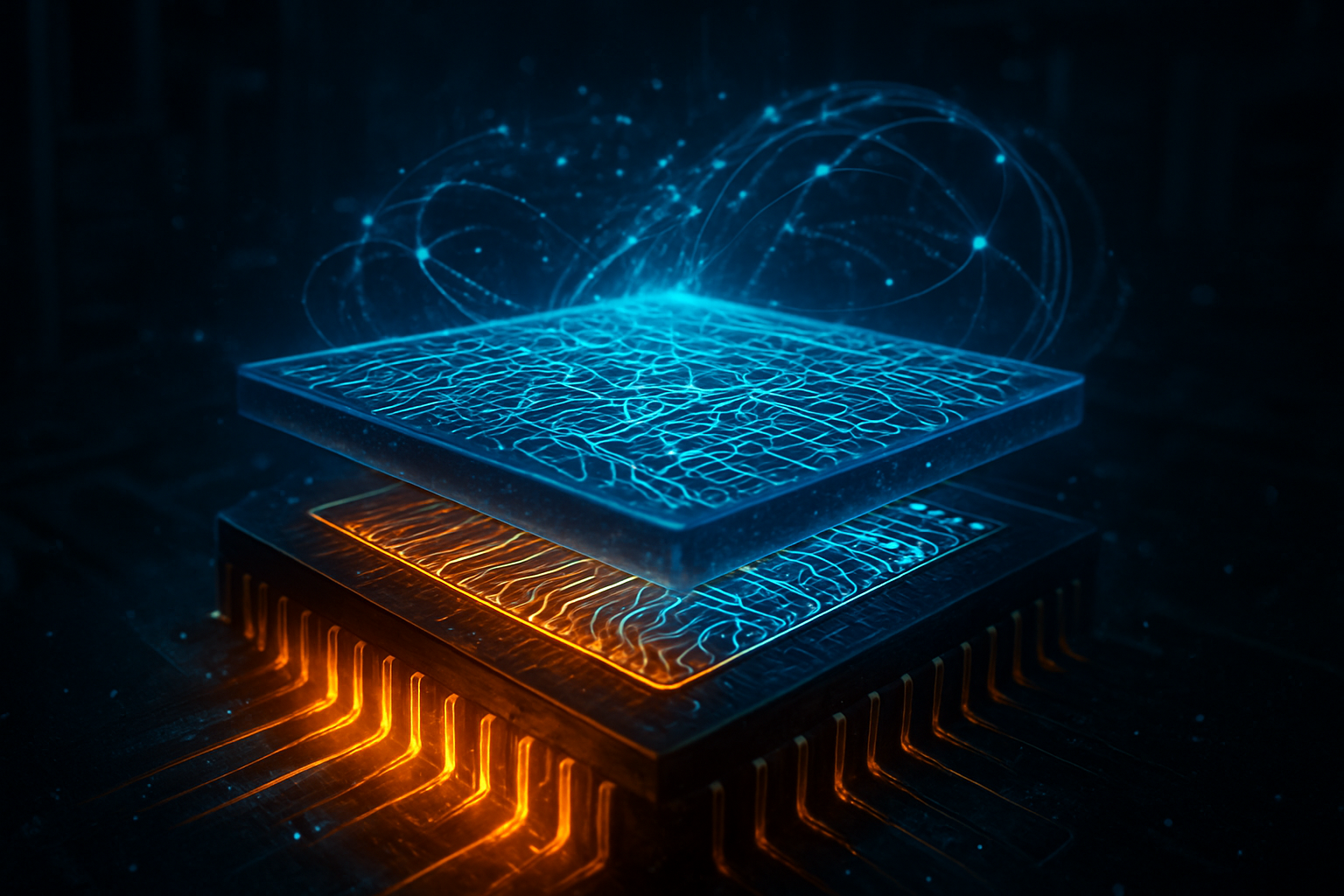
The Nanosheet Revolution: Engineering the 2nm Breakthrough
The technical centerpiece of the N2 node is the transition from the long-standing FinFET (Fin Field-Effect Transistor) architecture to Gate-All-Around (GAA) technology, which TSMC refers to as "Nanosheet" transistors. In previous FinFET designs, the gate covered three sides of the channel. However, as transistors shrunk toward the 2nm limit, electron leakage became an insurmountable hurdle. The Nanosheet design solves this by wrapping the gate entirely around the channel on all four sides. This provides superior electrostatic control, virtually eliminating current leakage and allowing for significantly lower operating voltages.
Beyond the transistor geometry, TSMC has introduced a proprietary feature known as NanoFlex™. This technology allows chip designers at firms like Apple (NASDAQ: AAPL) and NVIDIA (NASDAQ: NVDA) to mix and match different standard cell types—short cells for power efficiency and tall cells for peak performance—on a single die. This granular control over the power-performance-area (PPA) profile is unprecedented. Early reports from January 2026 indicate that TSMC has achieved logic test chip yields between 70% and 80%, a remarkable feat that places them well ahead of competitors like Samsung (KRX: 005930), whose 2nm GAA yields are reportedly struggling in the 40-55% range.
In terms of raw performance, the N2 process is delivering a 10% to 15% speed increase at the same power level compared to the refined 3nm (N3E) process. Perhaps more importantly for mobile and edge AI applications, it offers a 25% to 30% reduction in power consumption at the same clock speed. This efficiency gain is the primary driver for the massive industry interest, as it allows for more complex AI processing to occur on-device without devastating battery life or thermal envelopes.
The 2026 Capacity Crunch: Apple and NVIDIA Lead the Charge
The scramble for 2nm capacity has created a "supply choke" that has defined the early months of 2026. Industry insiders confirm that TSMC’s N2 capacity is effectively fully booked through the end of the year, with Apple and NVIDIA emerging as the dominant stakeholders. Apple has reportedly secured over 50% of the initial 2nm output, which it plans to utilize for its upcoming A20 Bionic chips in the iPhone 18 series and the M6 series processors for its MacBook Pro and iPad Pro lineups. For Apple, this exclusivity ensures that its "Apple Intelligence" ecosystem remains the gold standard for on-device AI performance.
NVIDIA has also made an aggressive play for 2nm wafers to power its "Rubin" GPU platform. As generative AI workloads continue to grow exponentially, NVIDIA’s move to 2nm is seen as a strategic necessity to maintain its dominance in the data center. By moving to the N2 node, NVIDIA can pack more CUDA cores and specialized AI accelerators into a single chip while staying within the power limits of modern liquid-cooled server racks. This has placed smaller AI startups and rival chipmakers in a precarious position, as they must compete for the remaining "leftover" capacity or wait for the 2nm ramp-up to reach 140,000 wafers per month by late 2026.
The cost of this technological edge is steep. Wafers for the 2nm process are currently estimated at $30,000 each, a 20% premium over the 3nm generation. This pricing reinforces a "winners-take-all" market dynamic, where only the wealthiest tech giants can afford the most advanced silicon. For consumers, this likely translates to higher price points for flagship hardware, but for the industry, it represents the massive capital expenditure required to keep the AI revolution moving forward.
Redefining the AI Landscape: Sustainability and Sovereignty
The shift to 2nm has implications that reach far beyond faster smartphones. In the broader AI landscape, the improved power efficiency of N2 is a critical component of the industry’s "green AI" initiatives. As data centers consume an ever-increasing percentage of global electricity, the 30% power reduction offered by 2nm chips becomes a vital tool for sustainability. This allows major cloud providers to expand their AI training clusters without requiring a linear increase in energy infrastructure, mitigating some of the environmental concerns surrounding the AI boom.
Furthermore, the 2nm milestone solidifies TSMC’s role as the indispensable lynchpin of the global digital economy. As the only foundry currently capable of delivering high-yield 2nm GAA wafers at scale, TSMC’s technological lead has become a matter of national and corporate sovereignty. This has intensified the competitive pressure on Intel (NASDAQ: INTC) and Samsung to accelerate their own roadmaps. While Intel’s 18A process is beginning to gain traction, TSMC’s successful N2 rollout in early 2026 suggests that the "Taiwan Advantage" remains firmly in place for the foreseeable future.
However, the concentration of 2nm manufacturing in Taiwan remains a point of strategic anxiety for global markets. Despite TSMC’s expansion into Arizona and Japan, the most advanced 2nm "GigaFabs" are currently concentrated in Hsinchu and Kaohsiung. This geopolitical reality means that any disruption in the region would immediately halt the production of the world’s most advanced AI and consumer chips, a vulnerability that continues to drive investments in domestic chip manufacturing in the U.S. and Europe.
The Road to 1.6nm: Super PowerRail and the A16 Era
Even as N2 production ramps up, TSMC is already looking toward its next major leap: the A16 (1.6nm) node. Scheduled for high-volume manufacturing in the second half of 2026, A16 will introduce "Super PowerRail" (SPR) technology. This is TSMC’s proprietary implementation of a Backside Power Delivery Network (BSPDN). Traditionally, power and signal lines are bundled on the front side of a wafer. SPR moves the power delivery to the back, connecting it directly to the transistor's source and drain.
This innovation is expected to free up nearly 20% more space for signal routing on the front side, significantly reducing "IR drop" (voltage loss) and improving power delivery efficiency. Experts predict that A16 will provide an additional 8% to 10% speed boost over N2P (the performance-enhanced version of 2nm). However, moving the power network to the backside presents a new set of thermal management challenges, as the chip's ability to spread heat laterally is reduced. This will likely necessitate new cooling solutions, such as microfluidic channels integrated directly into the chip packaging.
Looking ahead, the successful deployment of Super PowerRail in the A16 process will be the defining technical challenge of 2027. If TSMC can solve the thermal hurdles associated with backside power, it will pave the way for chips that are not only smaller but fundamentally more efficient at handling the high-intensity, continuous compute required for real-time AI reasoning and 8K holographic rendering.
Conclusion: A New Era of Silicon Dominance
TSMC’s 2nm production milestone is a watershed moment in the history of computing. By successfully navigating the transition from FinFET to Nanosheet architecture, the company has provided the world’s leading technology companies with the tools needed to push AI beyond current limitations. The fact that 2026 capacity is already spoken for by Apple and NVIDIA underscores the desperate industry-wide need for more efficient, more powerful silicon.
As we move through the first quarter of 2026, the key metrics to watch will be the continued stabilization of N2 yields and the first real-world benchmarks from 2nm-equipped devices. While the A16 roadmap and Super PowerRail technology promise even greater gains, the current focus remains on the flawless execution of N2. For the AI industry, the message is clear: the hardware bottleneck is widening, but the price of entry into the elite tier of performance has never been higher. TSMC's achievement ensures that the momentum of the AI era continues unabated, firmly establishing the 2nm node as the backbone of the next generation of digital innovation.
This content is intended for informational purposes only and represents analysis of current AI developments.
TokenRing AI delivers enterprise-grade solutions for multi-agent AI workflow orchestration, AI-powered development tools, and seamless remote collaboration platforms.
For more information, visit https://www.tokenring.ai/.