Tag: AI Hardware

  • MOCVD Systems Propel Semiconductor Innovation: Veeco’s Lumina+ Lights Up the Future of Compound Materials

    MOCVD Systems Propel Semiconductor Innovation: Veeco’s Lumina+ Lights Up the Future of Compound Materials

    In a landscape increasingly dominated by the demand for faster, more efficient, and smaller electronic components, the often-unsung hero of advanced manufacturing, Metal Organic Chemical Vapor Deposition (MOCVD) technology, continues its relentless march of innovation. On the cusp of this advancement is Veeco Instruments Inc. (NASDAQ: VECO), whose new Lumina+ MOCVD system, launched this October 2025, is poised to significantly accelerate the production of high-performance compound semiconductors, critical for everything from next-generation AI hardware to advanced displays and 5G networks.

    MOCVD systems are the foundational bedrock upon which many of today's most sophisticated electronic and optoelectronic devices are built. By precisely depositing atomic layers of material, these systems enable the creation of compound semiconductors—materials composed of two or more elements, unlike traditional silicon. These specialized materials offer unparalleled advantages in speed, frequency handling, temperature resilience, and light conversion efficiency, making them indispensable for the future of technology.

    Precision Engineering: Unpacking the Lumina+ Advancement

    MOCVD, also known as Metal-Organic Vapor Phase Epitaxy (MOVPE), is a sophisticated chemical vapor deposition method. It operates by introducing a meticulously controlled gas stream of 'precursors'—molecules like trimethylgallium, trimethylindium, and ammonia—into a reaction chamber. Within this chamber, semiconductor wafers are heated to extreme temperatures, typically between 400°C and 1300°C. This intense heat causes the precursors to decompose, depositing ultra-thin, single-crystal layers onto the wafer surface. The precise control over precursor concentrations allows for the growth of diverse material layers, enabling the fabrication of complex device structures.

    This technology is paramount for manufacturing III-V (e.g., Gallium Nitride (GaN), Gallium Arsenide (GaAs), Indium Phosphide (InP)) and II-VI compound semiconductors. These materials are not just alternatives to silicon; they are enablers of advanced functionalities. Their superior electron mobility, ability to operate at high frequencies and temperatures, and efficient light-to-electricity conversion properties make them essential for a vast array of high-performance applications. These include all forms of Light Emitting Diodes (LEDs), from general lighting to mini and micro-LEDs for advanced displays; various lasers like VCSELs for 3D sensing and LiDAR; power electronics utilizing GaN and Silicon Carbide (SiC) for electric vehicles and 5G infrastructure; high-efficiency solar cells; and high-speed RF devices crucial for modern telecommunications. The ability to deposit films less than one nanometer thick ensures unparalleled material quality and compositional control, directly translating to superior device performance.

    Veeco's Lumina+ MOCVD system marks a significant leap in this critical manufacturing domain. Building on the company's proprietary TurboDisc® technology, the Lumina+ introduces several breakthrough advancements. Notably, it boasts the industry's largest arsenic phosphide (As/P) batch size, which directly translates to reduced manufacturing costs and increased output. This, combined with best-in-class throughput and the lowest cost per wafer, sets a new benchmark for efficiency. The system also delivers industry-leading uniformity and repeatability across large As/P batches, a persistent challenge in high-precision semiconductor manufacturing. A key differentiator is its capability to deposit high-quality As/P epitaxial layers on wafers up to eight inches (200mm) in diameter, a substantial upgrade from previous generations limited to 6-inch wafers. This larger wafer size significantly boosts production capacity, as exemplified by Rocket Lab, a long-time Veeco customer, which plans to double its space-grade solar cell production capacity using the Lumina+ system. The enhanced process efficiency, coupled with Veeco's proven uniform injection and thermal control technology, ensures low defectivity and exceptional yield over long production campaigns.

    Reshaping the Competitive Landscape for Tech Innovators

    The continuous innovation in MOCVD systems, particularly exemplified by Veeco's Lumina+, has profound implications for a wide spectrum of technology companies, from established giants to nimble startups. Companies at the forefront of AI development, including those designing advanced machine learning accelerators and specialized AI hardware, stand to benefit immensely. Compound semiconductors, with their superior electron mobility and power efficiency, are increasingly vital for pushing the boundaries of AI processing power beyond what traditional silicon can offer.

    The competitive landscape is set to intensify, as companies that adopt these cutting-edge MOCVD technologies will gain a significant manufacturing advantage. This enables them to produce more sophisticated, higher-performance, and more energy-efficient devices at a lower cost per unit. For consumer electronics, this means advancements in smartphones, 4K and 8K displays, augmented/virtual reality (AR/VR) devices, and sophisticated 3D sensing and LiDAR applications. In telecommunications, the enhanced capabilities are critical for the rollout and optimization of 5G networks and high-speed data communication infrastructure. The automotive industry will see improvements in electric vehicle performance, autonomous driving systems, and advanced sensor technologies. Furthermore, sectors like aerospace and defense, renewable energy, and data centers will leverage these materials for high-efficiency solar cells, robust RF devices, and advanced power management solutions. Veeco (NASDAQ: VECO) itself stands to benefit directly from the increased demand for its innovative MOCVD platforms, solidifying its market positioning as a key enabler of advanced semiconductor manufacturing.

    Broader Implications: A Catalyst for a New Era of Electronics

    The advancements in MOCVD technology, spearheaded by systems like the Lumina+, are not merely incremental improvements; they represent a fundamental shift in the broader technological landscape. These innovations are critical for transcending the limitations of silicon-based electronics in areas where compound semiconductors offer inherent advantages. This aligns perfectly with the overarching trend towards more specialized hardware for specific computational tasks, particularly in the burgeoning field of AI.

    The impact of these MOCVD breakthroughs will be pervasive. We can expect to see a new generation of devices that are not only faster and more powerful but also significantly more energy-efficient. This has profound implications for environmental sustainability and the operational costs of data centers and other power-intensive applications. While the initial capital investment for MOCVD systems can be substantial, the long-term benefits in terms of device performance, efficiency, and expanded capabilities far outweigh these costs. This evolution can be compared to past milestones such as the advent of advanced lithography, which similarly enabled entire new industries and transformed existing ones. The ability to grow complex, high-quality compound semiconductor layers with unprecedented precision is a foundational advancement that will underpin many of the technological marvels of the coming decades.

    The Road Ahead: Anticipating Future Developments

    Looking to the future, the continuous innovation in MOCVD technology promises a wave of transformative developments. In the near term, we can anticipate the widespread adoption of even more efficient and advanced LED and Micro-LED technologies, leading to brighter, more color-accurate, and incredibly energy-efficient displays across various markets. The ability to produce higher power and frequency RF devices will further enable next-generation wireless communication and high-frequency applications, pushing the boundaries of connectivity. Advanced sensors, crucial for sophisticated 3D sensing, biometric applications, and LiDAR, will see significant enhancements, improving capabilities in automotive safety and consumer interaction.

    Longer term, compound semiconductors grown via MOCVD are poised to play a pivotal role in emerging computing paradigms. They offer a promising pathway to overcome the inherent limitations of traditional silicon in areas like neuromorphic computing, which aims to mimic the human brain's structure, and quantum computing, where high-speed and power efficiency are paramount. Furthermore, advancements in silicon photonics and optical data communication will enhance the integration of photonic devices into consumer electronics and data infrastructure, leading to unprecedented data transfer speeds. Challenges remain, including the need for continued cost reduction, scaling to even larger wafer sizes beyond 8-inch, and the integration of novel material combinations. However, experts predict substantial growth in the MOCVD equipment market, underscoring the increasing demand and the critical role these technologies will play in shaping the future of electronics.

    A New Era of Material Science and Device Performance

    In summary, the continuous innovation in MOCVD systems is a cornerstone of modern semiconductor manufacturing, enabling the creation of high-performance compound semiconductors that are critical for the next wave of technological advancement. Veeco's Lumina+ system, with its groundbreaking capabilities in batch size, throughput, uniformity, and 8-inch wafer processing, stands as a testament to this ongoing evolution. It is not merely an improvement but a catalyst, poised to unlock new levels of performance and efficiency across a multitude of industries.

    This development signifies a crucial step in the journey beyond traditional silicon, highlighting the increasing importance of specialized materials for specialized applications. The ability to precisely engineer materials at the atomic level is fundamental to powering the complex demands of artificial intelligence, advanced communication, and immersive digital experiences. As we move forward, watching for further innovations in MOCVD technology, the adoption rates of larger wafer sizes, and the emergence of novel applications leveraging these advanced materials will be key indicators of the trajectory of the entire tech industry in the coming weeks and months. The future of high-performance electronics is intrinsically linked to the continued sophistication of MOCVD.

    This content is intended for informational purposes only and represents analysis of current AI developments.

    TokenRing AI delivers enterprise-grade solutions for multi-agent AI workflow orchestration, AI-powered development tools, and seamless remote collaboration platforms.
    For more information, visit https://www.tokenring.ai/.

  • Veeco’s Lumina+ MOCVD System Ignites New Era for Compound Semiconductor Production, Fueling Next-Gen AI Hardware

    Veeco’s Lumina+ MOCVD System Ignites New Era for Compound Semiconductor Production, Fueling Next-Gen AI Hardware

    Veeco (NASDAQ: VECO) has today, October 6, 2025, unveiled its groundbreaking Lumina+ MOCVD System, a significant leap forward in the manufacturing of compound semiconductors. This announcement is coupled with a pivotal multi-tool order from Rocket Lab Corporation (NYSE: RKLB), signaling a robust expansion in high-volume production capabilities for critical electronic components. The Lumina+ system is poised to redefine efficiency and scalability in the compound semiconductor market, impacting everything from advanced AI hardware to space-grade solar cells, and laying a crucial foundation for the future of high-performance computing.

    A New Benchmark in Semiconductor Manufacturing

    The Lumina+ MOCVD system represents a culmination of advanced engineering, building upon Veeco's established Lumina platform and proprietary TurboDisc® technology. At its core, the system boasts the industry's largest arsenic phosphide (As/P) batch size, a critical factor for driving down manufacturing costs and increasing output. This innovation translates into best-in-class throughput and the lowest cost per wafer, setting a new benchmark for efficiency in compound semiconductor production. Furthermore, the Lumina+ delivers industry-leading uniformity and repeatability for As/P processes, ensuring consistent quality across large batches – a persistent challenge in high-precision semiconductor manufacturing.

    What truly sets the Lumina+ apart from previous generations and competing technologies is its enhanced process efficiency, which combines proven TurboDisc technology with breakthrough advancements in material deposition. This allows for the deposition of high-quality As/P epitaxial layers on wafers up to eight inches in diameter, a substantial improvement that broadens the scope of applications. Proprietary technology within the system ensures uniform injection and thermal control, vital for achieving excellent thickness and compositional uniformity in the epitaxial layers. Coupled with the Lumina platform's reputation for low defectivity over long campaigns, the Lumina+ promises exceptional yield and flexibility, directly addressing the demands for more robust and reliable semiconductor components. Initial reactions from industry experts highlight the system's potential to significantly accelerate the adoption of compound semiconductors in mainstream applications, particularly where silicon-based solutions fall short in performance or efficiency.

    Competitive Edge for AI and Tech Giants

    The launch of Veeco's Lumina+ MOCVD System and the subsequent multi-tool order from Rocket Lab (NYSE: RKLB) carry profound implications for AI companies, tech giants, and burgeoning startups. Companies heavily reliant on high-performance computing, such as those developing advanced AI models, machine learning accelerators, and specialized AI hardware, stand to benefit immensely. Compound semiconductors, known for their superior electron mobility, optical properties, and power efficiency compared to traditional silicon, are crucial for next-generation AI processors, high-speed optical interconnects, and efficient power management units.

    Tech giants like NVIDIA (NASDAQ: NVDA), Intel (NASDAQ: INTC), and AMD (NASDAQ: AMD), which are deeply invested in AI hardware development, could see accelerated innovation through improved access to these advanced materials. Faster, more efficient chips enabled by Lumina+ technology could lead to breakthroughs in AI training speeds, inference capabilities, and the overall energy efficiency of data centers, addressing a growing concern within the AI community. For startups focusing on niche AI applications requiring ultra-fast data processing or specific optical sensing capabilities (e.g., LiDAR for autonomous vehicles), the increased availability and reduced cost per wafer could lower barriers to entry and accelerate product development. This development could also disrupt existing supply chains, as companies might pivot towards compound semiconductor-based solutions where performance gains outweigh initial transition costs. Veeco's strategic advantage lies in providing the foundational manufacturing technology that unpins these advancements, positioning itself as a critical enabler in the ongoing AI hardware race.

    Wider Implications for the AI Landscape and Beyond

    Veeco's Lumina+ MOCVD System launch fits squarely into the broader trend of seeking increasingly specialized and high-performance materials to push the boundaries of technology, particularly in the context of AI. As AI models grow in complexity and demand more computational power, the limitations of traditional silicon are becoming more apparent. Compound semiconductors offer a pathway to overcome these limitations, providing higher speeds, better power efficiency, and superior optical and RF properties essential for advanced AI applications like neuromorphic computing, quantum computing components, and sophisticated sensor arrays.

    The multi-tool order from Rocket Lab (NYSE: RKLB), specifically for expanding domestic production under the CHIPS and Science Act, underscores a significant geopolitical and economic impact. It highlights a global effort to secure critical semiconductor supply chains and reduce reliance on foreign manufacturing, a lesson learned from recent supply chain disruptions. This move is not just about technological advancement but also about national security and economic resilience. Potential concerns, however, include the initial capital investment required for companies to adopt these new manufacturing processes and the specialized expertise needed to work with compound semiconductors. Nevertheless, this milestone is comparable to previous breakthroughs in semiconductor manufacturing that enabled entirely new classes of electronic devices, setting the stage for a new wave of innovation in AI hardware and beyond.

    The Road Ahead: Future Developments and Challenges

    In the near term, experts predict a rapid integration of Lumina+ manufactured compound semiconductors into high-demand applications such as 5G/6G infrastructure, advanced automotive sensors (LiDAR), and next-generation displays (MicroLEDs). The ability to produce these materials at a lower cost per wafer and with higher uniformity will accelerate their adoption across these sectors. Long-term, the impact on AI could be transformative, enabling more powerful and energy-efficient AI accelerators, specialized processors for edge AI, and advanced photonics for optical computing architectures that could fundamentally change how AI is processed.

    Potential applications on the horizon include highly efficient power electronics for AI data centers, enabling significant reductions in energy consumption, and advanced VCSELs for ultra-fast data communication within and between AI systems. Challenges that need to be addressed include further scaling up production to meet anticipated demand, continued research into new compound semiconductor materials and their integration with existing silicon platforms, and the development of a skilled workforce capable of operating and maintaining these advanced MOCVD systems. Experts predict that the increased availability of high-quality compound semiconductors will unleash a wave of innovation, leading to AI systems that are not only more powerful but also more sustainable and versatile.

    A New Chapter in AI Hardware and Beyond

    Veeco's (NASDAQ: VECO) launch of the Lumina+ MOCVD System marks a pivotal moment in the evolution of semiconductor manufacturing, promising to unlock new frontiers for high-performance electronics, particularly in the rapidly advancing field of artificial intelligence. Key takeaways include the system's unprecedented batch size, superior throughput, and industry-leading uniformity, all contributing to a significantly lower cost per wafer for compound semiconductors. The strategic multi-tool order from Rocket Lab (NYSE: RKLB) further solidifies the immediate impact, ensuring expanded domestic production of critical components.

    This development is not merely an incremental improvement; it represents a foundational shift that will enable the next generation of AI hardware, from more efficient processors to advanced sensors and optical communication systems. Its significance in AI history will be measured by how quickly and effectively these advanced materials are integrated into AI architectures, potentially leading to breakthroughs in computational power and energy efficiency. In the coming weeks and months, the tech world will be watching closely for further adoption announcements, the performance benchmarks of devices utilizing Lumina+ produced materials, and how this new manufacturing capability reshapes the competitive landscape for AI hardware development. This content is intended for informational purposes only and represents analysis of current AI developments.

    TokenRing AI delivers enterprise-grade solutions for multi-agent AI workflow orchestration, AI-powered development tools, and seamless remote collaboration platforms.
    For more information, visit https://www.tokenring.ai/.

  • Cambridge Scientists Uncover Quantum Secret: A Solar Power Revolution in the Making

    Cambridge Scientists Uncover Quantum Secret: A Solar Power Revolution in the Making

    Cambridge scientists have made a monumental breakthrough in solar energy, unveiling a novel organic semiconductor material named P3TTM that harnesses a previously unobserved quantum phenomenon. This discovery, reported in late 2024 and extensively covered in October 2025, promises to fundamentally revolutionize solar power by enabling the creation of single-material solar cells that are significantly more efficient, lighter, and cheaper than current technologies. Its immediate significance lies in simplifying solar cell design, drastically reducing manufacturing complexity and cost, and opening new avenues for flexible and integrated solar applications, potentially accelerating the global transition to sustainable energy.

    Unlocking Mott-Hubbard Physics in Organic Semiconductors

    The core of this groundbreaking advancement lies in the unique properties of P3TTM, a spin-radical organic semiconductor molecule developed through a collaborative effort between Professor Hugo Bronstein's chemistry team and Professor Sir Richard Friend's semiconductor physics group at the University of Cambridge. P3TTM is distinguished by having a single unpaired electron at its core, which imbues it with unusual electronic and magnetic characteristics. The "quantum secret" is the observation that when P3TTM molecules are closely packed, they exhibit Mott-Hubbard physics – a phenomenon previously believed to occur exclusively in complex inorganic materials.

    This discovery challenges a century-old understanding of quantum mechanics in materials science. In P3TTM, the unpaired electrons align in an alternating "up, down, up, down" pattern. When light strikes these molecules, an electron can "hop" from its original position to an adjacent molecule, leaving behind a positive charge. This intrinsic charge separation mechanism within a homogeneous molecular lattice is what sets P3TTM apart. Unlike conventional organic solar cells, which require at least two different materials (an electron donor and an electron acceptor) to facilitate charge separation, P3TTM can generate charges by itself. This simplifies the device architecture dramatically and leads to what researchers describe as "close-to-unity charge collection efficiency," meaning almost every absorbed photon is converted into usable electricity.

    Initial reactions from the AI research community and industry experts have been overwhelmingly positive. This discovery is not only seen as a significant advancement for solar energy but also as a "critical enabler for the next generation of AI." Experts anticipate that P3TTM technology could lead to significantly lower power consumption for AI accelerators and edge computing devices, signaling a potential "beyond silicon" era. This fundamental shift could contribute substantially to the "Green AI" movement, which aims to address the burgeoning energy consumption of AI systems.

    Reshaping the Competitive Landscape for Tech Giants and Startups

    The P3TTM breakthrough is poised to send ripples across multiple industries, creating both immense opportunities and significant competitive pressures. Companies specializing in organic electronics and material science are in a prime position to gain a first-mover advantage, potentially redefining their market standing through early investment or licensing of P3TTM-like technologies.

    For traditional solar panel manufacturers like JinkoSolar and Vikram Solar, this technology offers a pathway to drastically reduce manufacturing complexity and costs, leading to lighter, simpler, and more cost-effective solar products. This could enable them to diversify their offerings and penetrate new markets with flexible and integrated solar solutions.

    The impact extends powerfully into the AI hardware sector. Companies focused on neuromorphic computing, such such as Intel (NASDAQ: INTC) with its Loihi chip and IBM (NYSE: IBM) with TrueNorth, could integrate these novel organic materials to enhance their brain-inspired AI accelerators. Major tech giants like NVIDIA (NASDAQ: NVDA) (for GPUs), Google (NASDAQ: GOOGL) (for custom TPUs), Amazon (NASDAQ: AMZN), and Microsoft (NASDAQ: MSFT) (for cloud AI infrastructure) face a strategic imperative: aggressively invest in R&D for organic Mott-Hubbard materials or risk being outmaneuvered. The high energy consumption of large-scale AI is a growing environmental concern, and P3TTM offers a pathway to "green AI" hardware, providing a significant competitive advantage for companies committed to sustainability.

    The lower capital requirements for manufacturing organic semiconductors could empower startups to innovate in AI hardware without the prohibitive costs associated with traditional silicon foundries, fostering a wave of new entrants, especially in flexible and edge AI devices. Furthermore, manufacturers of IoT, wearable electronics, and flexible displays stand to benefit immensely from the inherent flexibility, lightweight nature, and low-power characteristics of organic semiconductors, enabling new product categories like self-powered sensors and wearable AI assistants.

    Broader Implications for Sustainable AI and Energy

    The Cambridge quantum solar discovery of P3TTM represents a pivotal moment in material science and energy, fundamentally altering our understanding of charge generation in organic materials. This breakthrough fits perfectly into the broader AI landscape and trends, particularly the urgent drive towards sustainable and energy-efficient AI solutions. The immense energy footprint of modern AI necessitates radical innovations in renewable energy, and P3TTM offers a promising avenue to power these systems with unprecedented environmental efficiency.

    Beyond direct energy generation, the ability to engineer complex quantum mechanical behaviors into organic materials suggests novel pathways for developing "next-generation energy-efficient AI computing" and AI hardware. This could lead to new types of computing components or energy harvesting systems directly embedded within AI infrastructure, significantly reducing the energy overhead associated with current AI systems.

    The implications for energy and technology are transformative. P3TTM could fundamentally reshape the solar energy industry by enabling the production of lighter, simpler, more flexible, and potentially much cheaper solar panels. The understanding gained from P3TTM could also lead to breakthroughs in other fields, such as optoelectronics and self-charging electronics.

    However, potential concerns remain. Scalability and commercialization present typical challenges for any nascent, groundbreaking technology. Moving from laboratory demonstration to widespread commercialization will require significant engineering efforts and investment. Long-term stability and durability, historically a challenge for organic solar cells, will need thorough evaluation. While P3TTM offers near-perfect charge collection efficiency, its journey from lab to widespread adoption will depend on addressing these practical hurdles. This discovery is comparable to historical energy milestones like the development of crystalline silicon solar cells, representing not just an incremental improvement but a foundational shift. In the AI realm, it aligns with breakthroughs like deep learning, by finding a new physical mechanism that could enable more powerful and sustainable AI systems.

    The Road Ahead: Challenges and Predictions

    The path from a groundbreaking laboratory discovery like P3TTM to widespread commercial adoption is often long and complex. In the near term, researchers will focus on further optimizing the P3TTM molecule for stability and performance under various environmental conditions. Efforts will also be directed towards scaling up the synthesis of P3TTM and developing cost-effective manufacturing processes for single-material solar cells. The "drop-in" nature, if it can be maintained, for integration into existing manufacturing lines could significantly accelerate adoption.

    Long-term developments include exploring the full potential of Mott-Hubbard physics in other organic materials to discover even more efficient or specialized semiconductors. Experts predict that the ability to engineer quantum phenomena in organic materials will open doors to a new class of optoelectronic devices, including highly efficient light-emitting diodes and advanced sensors. The integration of P3TTM-enabled flexible solar cells into everyday objects, such as self-powered smart textiles, building facades, and portable electronics, is a highly anticipated application.

    Challenges that need to be addressed include improving the long-term operational longevity and durability of organic semiconductors to match or exceed that of conventional silicon. Ensuring the environmental sustainability of P3TTM's production at scale, from raw material sourcing to end-of-life recycling, will also be crucial. Furthermore, the economic advantage of P3TTM over established solar technologies will need to be clearly demonstrated to drive market adoption.

    Experts predict a future where quantum materials like P3TTM play a critical role in addressing global energy demands sustainably. The quantum ecosystem is expected to mature, with increased collaboration between material science and AI firms. Quantum-enhanced models could significantly improve the accuracy of energy market forecasting and the operation of renewable energy plants. The focus will not only be on efficiency but also on designing future solar panels to be easily recyclable and to have increased durability for longer useful lifetimes, minimizing environmental impact for decades to come.

    A New Dawn for Solar and Sustainable AI

    The discovery of the P3TTM organic semiconductor by Cambridge scientists marks a profound turning point in the quest for sustainable energy and efficient AI. By uncovering a "quantum secret" – the unexpected manifestation of Mott-Hubbard physics in an organic material – researchers have unlocked a pathway to solar cells that are not only dramatically simpler and cheaper to produce but also boast near-perfect charge collection efficiency. This represents a foundational shift, "writing a new chapter in the textbook" of solar energy.

    The significance of this development extends far beyond just solar panels. It offers a tangible "beyond silicon" route for energy-efficient AI hardware, critically enabling the "Green AI" movement and potentially revolutionizing how AI systems are powered and deployed. The ability to integrate flexible, lightweight, and highly efficient solar cells into a myriad of devices could transform industries from consumer electronics to smart infrastructure.

    As we move forward, the coming weeks and months will be critical for observing how this laboratory breakthrough transitions into scalable, commercially viable solutions. Watch for announcements regarding pilot projects, strategic partnerships between material science companies and solar manufacturers, and further research into the long-term stability and environmental impact of P3TTM. This quantum leap by Cambridge scientists signals a new dawn, promising a future where clean energy and powerful, sustainable AI are more intertwined than ever before.

    This content is intended for informational purposes only and represents analysis of current AI developments.

    TokenRing AI delivers enterprise-grade solutions for multi-agent AI workflow orchestration, AI-powered development tools, and seamless remote collaboration platforms.
    For more information, visit https://www.tokenring.ai/

  • AI Fuels Semiconductor Supercycle: Entegris Emerges as a Critical Enabler Amidst Investment Frenzy

    AI Fuels Semiconductor Supercycle: Entegris Emerges as a Critical Enabler Amidst Investment Frenzy

    The global semiconductor industry is in the throes of an unprecedented investment surge, largely propelled by the insatiable demand for Artificial Intelligence (AI) and high-performance computing (HPC). As of October 5, 2025, this robust recovery is setting the stage for substantial market expansion, with projections indicating a global semiconductor market reaching approximately $697 billion this year, an 11% increase from 2024. This burgeoning market is expected to hit a staggering $1 trillion by 2030, underscoring AI's transformative power across the tech landscape.

    Amidst this supercycle, Entegris, Inc. (NASDAQ: ENTG), a vital supplier of advanced materials and process solutions, has strategically positioned itself to capitalize on these trends. The company has demonstrated strong financial performance, securing significant U.S. CHIPS Act funding and announcing a massive $700 million domestic investment in R&D and manufacturing. This, coupled with substantial increases in institutional stakes from major players like Vanguard Group Inc., Principal Financial Group Inc., and Goldman Sachs Group Inc., signals a profound confidence in Entegris's indispensable role in enabling next-generation AI technologies and the broader semiconductor ecosystem. The immediate significance of these movements points to a sustained, AI-driven growth phase for semiconductors, a prioritization of advanced manufacturing capabilities, and a strategic reshaping of global supply chains towards greater resilience and domestic self-reliance.

    The Microcosm of Progress: Advanced Materials and Manufacturing at AI's Core

    The current AI revolution is intrinsically linked to groundbreaking advancements in semiconductor technology, where the pursuit of ever-smaller, more powerful, and energy-efficient chips is paramount. This technical frontier is defined by the relentless march towards advanced process nodes, sophisticated packaging, high-bandwidth memory, and innovative material science. The global semiconductor market's projected surge to $697 billion in 2025, with AI chips alone expected to generate over $150 billion in sales, vividly illustrates the immense focus on these critical areas.

    At the heart of this technical evolution are advanced process nodes, specifically 3nm and the rapidly emerging 2nm technology. These nodes are vital for AI as they dramatically increase transistor density on a chip, leading to unprecedented computational power and significantly improved energy efficiency. While 3nm technology is already powering advanced processors, TSMC's 2nm chip, introduced in April 2025 with mass production slated for late 2025, promises a 10-15% boost in computing speed at the same power or a 20-30% reduction in power usage. This leap is achieved through Gate-All-Around (GAA) or nanosheet transistor architectures, which offer superior gate control compared to older planar designs, and relies on complex Extreme Ultraviolet (EUV) lithography – a stark departure from less demanding techniques of prior generations. These advancements are set to supercharge AI applications from real-time language translation to autonomous systems.

    Complementing smaller nodes, advanced packaging has emerged as a critical enabler, overcoming the physical limits and escalating costs of traditional transistor scaling. Techniques like 2.5D packaging, exemplified by TSMC's CoWoS (Chip-on-Wafer-on-Substrate), integrate multiple chips (e.g., GPUs and HBM stacks) on a silicon interposer, drastically reducing data travel distance and improving communication speed and energy efficiency. More ambitiously, 3D stacking vertically integrates wafers and dies using Through-Silicon Vias (TSVs), offering ultimate density and efficiency. AI accelerator chips utilizing 3D stacking have demonstrated a 50% improvement in performance per watt, a crucial metric for AI training models and data centers. These methods fundamentally differ from traditional 2D packaging by creating ultra-wide, extremely short communication buses, effectively shattering the "memory wall" bottleneck.

    High-Bandwidth Memory (HBM) is another indispensable component for AI and HPC systems, delivering unparalleled data bandwidth, lower latency, and superior power efficiency. Following HBM3 and HBM3E, the JEDEC HBM4 specification, finalized in April 2025, doubles the interface width to 2048-bits and specifies a maximum data rate of 8 Gb/s, translating to a staggering 2.048 TB/s memory bandwidth per stack. This 3D-stacked DRAM technology, with up to 16-high configurations, offers capacities up to 64GB in a single stack, alongside improved power efficiency. This represents a monumental leap from traditional DDR4 or GDDR5, crucial for the massive data throughput demanded by complex AI models.

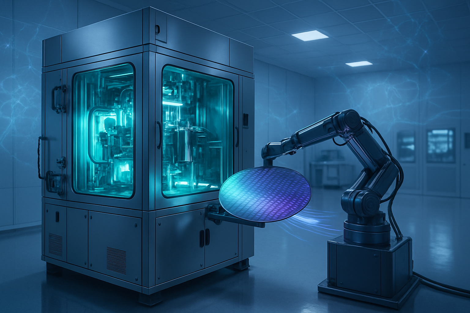
    Crucially, material science innovations are pivotal. Molybdenum (Mo) is transforming advanced metallization, particularly for 3D architectures. Its substantially lower electrical resistance in nano-scale interconnects, compared to tungsten, is vital for signals traversing hundreds of vertical layers. Companies like Lam Research (NASDAQ: LRCX) have introduced specialized tools, ALTUS Halo for deposition and Akara for etching, to facilitate molybdenum's mass production. This breakthrough mitigates resistance issues at an atomic scale, a fundamental roadblock for dense 3D chips. Entegris (NASDAQ: ENTG) is a foundational partner in this ecosystem, providing essential materials solutions, microcontamination control products (like filters capturing contaminants down to 1nm), and advanced materials handling systems (such as FOUPs) that are indispensable for achieving the high yields and reliability required for these cutting-edge processes. Their significant R&D investments, partly bolstered by CHIPS Act funding, directly support the miniaturization and performance requirements of future AI chips, enabling services that demand double the bandwidth and 40% improved power efficiency.

    The AI research community and industry experts have universally lauded these semiconductor advancements as foundational enablers. They recognize that this hardware evolution directly underpins the scale and complexity of current and future AI models, driving an "AI supercycle" where the global semiconductor market could exceed $1 trillion by 2030. Experts emphasize the hardware-dependent nature of the deep learning revolution, highlighting the critical role of advanced packaging for performance and efficiency, HBM for massive data throughput, and new materials like molybdenum for overcoming physical limitations. While acknowledging challenges in manufacturing complexity, high costs, and talent shortages, the consensus remains that continuous innovation in semiconductors is the bedrock upon which the future of AI will be built.

    Strategic Realignment: How Semiconductor Investments Reshape the AI Landscape

    The current surge in semiconductor investments, fueled by relentless innovation in advanced nodes, HBM4, and sophisticated packaging, is fundamentally reshaping the competitive dynamics across AI companies, tech giants, and burgeoning startups. As of October 5, 2025, the "AI supercycle" is driving an estimated $150 billion in AI chip sales this year, with significant capital expenditures projected to expand capacity and accelerate R&D. This intense focus on cutting-edge hardware is creating both immense opportunities and formidable challenges for players across the AI ecosystem.

    Leading the charge in benefiting from these advancements are the major AI chip designers and the foundries that manufacture their designs. NVIDIA Corp. (NASDAQ: NVDA) remains the undisputed leader, with its Blackwell architecture and GB200 NVL72 platforms designed for trillion-parameter models, leveraging the latest HBM and advanced interconnects. However, rivals like Advanced Micro Devices Inc. (NASDAQ: AMD) are gaining traction with their MI300 series, focusing on inference workloads and utilizing 2.5D interposers and 3D-stacked memory. Intel Corp. (NASDAQ: INTC) is also making aggressive moves with its Gaudi 3 AI accelerators and a significant $5 billion strategic partnership with NVIDIA for co-developing AI infrastructure, aiming to leverage its internal foundry capabilities and advanced packaging technologies like EMIB to challenge the market. The foundries themselves, particularly Taiwan Semiconductor Manufacturing Company Ltd. (NYSE: TSM) and Samsung Electronics Co., Ltd. (KRX: 005930), are indispensable, as their leadership in 2nm/1.4nm process nodes and advanced packaging solutions like CoWoS and I-Cube directly dictates the pace of AI innovation.

    The competitive landscape is further intensified by the hyperscale cloud providers—Alphabet Inc. (NASDAQ: GOOGL) (Google DeepMind), Amazon.com Inc. (NASDAQ: AMZN) (AWS), Microsoft Corp. (NASDAQ: MSFT), and Meta Platforms Inc. (NASDAQ: META)—who are heavily investing in custom silicon. Google's Tensor Processing Units (TPUs) and new Arm-based Axion CPUs, Amazon's Graviton4, Trainium, and Inferentia chips, and Microsoft's Azure Maia 100 and Cobalt 100 processors exemplify a strategic shift towards vertical integration. By designing their own AI chips, these tech giants gain significant advantages in performance, latency, cost-efficiency, and strategic control over their AI infrastructure, optimizing hardware and software specifically for their vast cloud-based AI workloads. This trend extends to major AI labs like OpenAI, which plans to launch its own custom AI chips by 2026, signaling a broader movement towards hardware optimization to fuel increasingly complex AI models.

    This strategic realignment also brings potential disruption. The dominance of general-purpose GPUs, while still critical for AI training, is being gradually challenged by specialized AI accelerators and custom ASICs, particularly for inference workloads. The prioritization of HBM production by memory manufacturers like SK Hynix Inc. (KRX: 000660), Samsung, and Micron Technology Inc. (NASDAQ: MU) could also influence the supply and pricing of less specialized memory. For startups, while leading-edge hardware remains expensive, the growing availability of cloud-based AI services powered by these advancements, coupled with the emergence of specialized AI-dedicated chips, offers new avenues for high-performance AI access. Foundational material suppliers like Entegris (NASDAQ: ENTG) play a critical, albeit often behind-the-scenes, role, providing the high-purity chemicals, advanced materials, and contamination control solutions essential for manufacturing these next-generation chips, thereby enabling the entire ecosystem. The strategic advantages now lie with companies that can either control access to cutting-edge manufacturing capabilities, design highly optimized custom silicon, or build robust software ecosystems around their hardware, thereby creating strong barriers to entry and fostering customer loyalty in this rapidly evolving AI-driven market.

    The Broader AI Canvas: Geopolitics, Supply Chains, and the Trillion-Dollar Horizon

    The current wave of semiconductor investment and innovation transcends mere technological upgrades; it fundamentally reshapes the broader AI landscape and global geopolitical dynamics. As of October 5, 2025, the "AI Supercycle" is propelling the semiconductor market towards an astounding $1 trillion valuation by 2030, a trajectory driven almost entirely by the escalating demands of artificial intelligence. This profound shift is not just about faster chips; it's about powering the next generation of AI, while simultaneously raising critical societal, economic, and geopolitical questions.

    These advancements are fueling AI development by enabling increasingly specialized and energy-efficient architectures. The industry is witnessing a dramatic pivot towards custom AI accelerators and Application-Specific Integrated Circuits (ASICs), designed for specific AI workloads in data centers and at the edge. Advanced packaging technologies, such as 2.5D/3D integration and hybrid bonding, are becoming the new frontier for performance gains as traditional transistor scaling slows. Furthermore, nascent fields like neuromorphic computing, which mimics the human brain for ultra-low power AI, and silicon photonics, using light for faster data transfer, are gaining traction. Ironically, AI itself is revolutionizing chip design and manufacturing, with AI-powered Electronic Design Automation (EDA) tools drastically accelerating design cycles and improving chip quality.

    The societal and economic impacts are immense. The projected $1 trillion semiconductor market underscores massive economic growth, driven by AI-optimized hardware across cloud, autonomous systems, and edge computing. This creates new jobs in engineering and manufacturing but also raises concerns about potential job displacement due to AI automation, highlighting the need for proactive reskilling and ethical frameworks. AI-driven productivity gains promise to reduce costs across industries, with "Physical AI" (autonomous robots, humanoids) expected to drive the next decade of innovation. However, the uneven global distribution of advanced AI capabilities risks widening existing digital divides, creating a new form of inequality.

    Amidst this progress, significant concerns loom. Geopolitically, the semiconductor industry is at the epicenter of a "Global Chip War," primarily between the United States and China, driven by the race for AI dominance and national security. Export controls, tariffs, and retaliatory measures are fragmenting global supply chains, leading to aggressive onshoring and "friendshoring" efforts, exemplified by the U.S. CHIPS and Science Act, which allocates over $52 billion to boost domestic semiconductor manufacturing and R&D. Energy consumption is another daunting challenge; AI-driven data centers already consume vast amounts of electricity, with projections indicating a 50% annual growth in AI energy requirements through 2030, potentially accounting for nearly half of total data center power. This necessitates breakthroughs in hardware efficiency to prevent AI scaling from hitting physical and economic limits. Ethical considerations, including algorithmic bias, privacy concerns, and diminished human oversight in autonomous systems, also demand urgent attention to ensure AI development aligns with human welfare.

    Comparing this era to previous technological shifts, the current period represents a move "beyond Moore's Law," where advanced packaging and heterogeneous integration are the new drivers of performance. It marks a deeper level of specialization than the rise of general-purpose GPUs, with a profound shift towards custom ASICs for specific AI tasks. Crucially, the geopolitical stakes are uniquely high, making control over semiconductor technology a central pillar of national security and technological sovereignty, reminiscent of historical arms races.

    The Horizon of Innovation: Future Developments in AI and Semiconductors

    The symbiotic relationship between AI and semiconductors is poised to accelerate innovation at an unprecedented pace, driving both fields into new frontiers. As of October 5, 2025, AI is not merely a consumer of advanced semiconductor technology but also a crucial tool for its development, design, and manufacturing. This dynamic interplay is widely recognized as the defining technological narrative of our time, promising transformative applications while presenting formidable challenges.

    In the near term (1-3 years), AI will continue to revolutionize chip design and optimization. AI-powered Electronic Design Automation (EDA) tools are drastically reducing chip design times, enhancing verification, and predicting performance issues, leading to faster time-to-market and lower development costs. Companies like Synopsys (NASDAQ: SNPS) are integrating generative AI into their EDA suites to streamline the entire chip development lifecycle. The relentless demand for AI is also solidifying 3nm and 2nm process nodes as the industry standard, with TSMC (NYSE: TSM), Samsung (KRX: 005930), and Rapidus leading efforts to produce these cutting-edge chips. The market for specialized AI accelerators, including GPUs, TPUs, NPUs, and ASICs, is projected to exceed $200 billion by 2025, driving intense competition and continuous innovation from players like NVIDIA (NASDAQ: NVDA), AMD (NASDAQ: AMD), and Google (NASDAQ: GOOGL). Furthermore, edge AI semiconductors, designed for low-power efficiency and real-time decision-making on devices, will proliferate in autonomous drones, smart cameras, and industrial robots. AI itself is optimizing manufacturing processes, with predictive maintenance, advanced defect detection, and real-time process adjustments enhancing precision and yield in semiconductor fabrication.

    Looking further ahead (beyond 3 years), more transformative changes are on the horizon. Neuromorphic computing, inspired by the human brain, promises drastically lower energy consumption for AI tasks, with players like Intel (NASDAQ: INTC) (Loihi 2) and IBM (NYSE: IBM) (TrueNorth) leading the charge. AI-driven computational material science will accelerate the discovery of new semiconductor materials with desired properties, expanding the materials funnel exponentially. The convergence of AI with quantum and optical computing could unlock problem-solving capabilities far beyond classical computing, potentially revolutionizing fields like drug discovery. Advanced packaging techniques will become even more essential, alongside innovations in ultra-fast interconnects to address data movement bottlenecks. A paramount long-term focus will be on sustainable AI chips to counter the escalating power consumption of AI systems, leading to energy-efficient designs and potentially fully autonomous manufacturing facilities managed by AI and robotics.

    These advancements will fuel a vast array of applications. Increasingly complex Generative AI and Large Language Models (LLMs) will be powered by highly efficient accelerators, enabling more sophisticated interactions. Fully autonomous vehicles, robotics, and drones will rely on advanced edge AI chips for real-time decision-making. Healthcare will benefit from immense computational power for personalized medicine and drug discovery. Smart cities and industrial automation will leverage AI-powered chips for predictive analytics and operational optimization. Consumer electronics will feature enhanced AI capabilities, offering more intelligent user experiences. Data centers, projected to account for 60% of the AI chip market by 2025, will continue to drive demand for high-performance AI chips for machine learning and natural language processing.

    However, significant challenges persist. The escalating complexity and cost of manufacturing chips at advanced nodes (3nm and below) pose substantial barriers. The burgeoning energy consumption of AI systems, with projections indicating a 50% annual growth through 2030, necessitates breakthroughs in hardware efficiency and heat dissipation. A deepening global talent shortage in the semiconductor industry, coupled with fierce competition for AI and machine learning specialists, threatens to impede innovation. Supply chain resilience remains a critical concern, vulnerable to geopolitical risks, trade tariffs, and a reliance on foreign components. Experts predict that the future of AI hinges on continuous hardware innovation, with the global semiconductor market potentially reaching $1.3 trillion by 2030, driven by generative AI. Leading companies like TSMC, NVIDIA, AMD, and Google are expected to continue driving this innovation. Addressing the talent crunch, diversifying supply chains, and investing in energy-efficient designs will be crucial for sustaining the rapid growth in this symbiotic relationship, with the potential for reconfigurable hardware to adapt to evolving AI algorithms offering greater flexibility.

    A New Silicon Age: AI's Enduring Legacy and the Road Ahead

    The semiconductor industry stands at the precipice of a new silicon age, entirely reshaped by the demands and advancements of Artificial Intelligence. The "AI Supercycle," as observed in late 2024 and throughout 2025, is characterized by unprecedented investment, rapid technical innovation, and profound geopolitical shifts, all converging to propel the global semiconductor market towards an astounding $1 trillion valuation by 2030. Key takeaways highlight AI as the dominant catalyst for this growth, driving a relentless pursuit of advanced manufacturing nodes like 2nm, sophisticated packaging solutions, and high-bandwidth memory such as HBM4. Foundational material suppliers like Entegris, Inc. (NASDAQ: ENTG), with its significant domestic investments and increasing institutional backing, are proving indispensable in enabling these cutting-edge technologies.

    This era marks a pivotal moment in AI history, fundamentally redefining the capabilities of intelligent systems. The shift towards specialized AI accelerators and custom silicon by tech giants—Alphabet Inc. (NASDAQ: GOOGL), Amazon.com Inc. (NASDAQ: AMZN), Microsoft Corp. (NASDAQ: MSFT), and Meta Platforms Inc. (NASDAQ: META)—alongside the continued dominance of NVIDIA Corp. (NASDAQ: NVDA) and the aggressive strategies of Advanced Micro Devices Inc. (NASDAQ: AMD) and Intel Corp. (NASDAQ: INTC), underscores a deepening hardware-software co-design paradigm. The long-term impact promises a future where AI is pervasive, powering everything from fully autonomous systems and personalized healthcare to smarter infrastructure and advanced generative models. However, this future is not without its challenges, including escalating energy consumption, a critical global talent shortage, and complex geopolitical dynamics that necessitate resilient supply chains and ethical governance.

    In the coming weeks and months, the industry will be watching closely for further advancements in 2nm and 1.4nm process node development, the widespread adoption of HBM4 across next-generation AI accelerators, and the continued strategic partnerships and investments aimed at securing manufacturing capabilities and intellectual property. The ongoing "Global Chip War" will continue to shape investment decisions and supply chain strategies, emphasizing regionalization efforts like those spurred by the U.S. CHIPS Act. Ultimately, the symbiotic relationship between AI and semiconductors will continue to be the primary engine of technological progress, demanding continuous innovation, strategic foresight, and collaborative efforts to navigate the opportunities and challenges of this transformative era.

    This content is intended for informational purposes only and represents analysis of current AI developments.

    TokenRing AI delivers enterprise-grade solutions for multi-agent AI workflow orchestration, AI-powered development tools, and seamless remote collaboration platforms.
    For more information, visit https://www.tokenring.ai/.

  • Beyond Moore’s Law: How Advanced Packaging is Unlocking the Next Era of AI Performance

    Beyond Moore’s Law: How Advanced Packaging is Unlocking the Next Era of AI Performance

    The relentless march of Artificial Intelligence demands ever-increasing computational power, blazing-fast data transfer, and unparalleled energy efficiency. As traditional silicon scaling, famously known as Moore's Law, approaches its physical and economic limits, the semiconductor industry is turning to a new frontier of innovation: advanced packaging technologies. These groundbreaking techniques are no longer just a back-end process; they are now at the forefront of hardware design, proving crucial for enhancing the performance and efficiency of chips that power the most sophisticated AI and machine learning applications, from large language models to autonomous systems.

    This shift represents an immediate and critical evolution in microelectronics. Without these innovations, the escalating demands of modern AI workloads—which are inherently data-intensive and latency-sensitive—would quickly outstrip the capabilities of conventional chip designs. Advanced packaging solutions are enabling the close integration of processing units and memory, dramatically boosting bandwidth, reducing latency, and overcoming the persistent "memory wall" bottleneck that has historically constrained AI performance. By allowing for higher computational density and more efficient power delivery, these technologies are directly fueling the ongoing AI revolution, making more powerful, energy-efficient, and compact AI hardware a reality.

    Technical Marvels: The Core of AI's Hardware Revolution

    The advancements in chip packaging are fundamentally redefining what's possible in AI hardware. These technologies move beyond the limitations of monolithic 2D designs to achieve unprecedented levels of performance, efficiency, and flexibility.

    2.5D Packaging represents an ingenious intermediate step, where multiple bare dies—such as a Graphics Processing Unit (GPU) and High-Bandwidth Memory (HBM) stacks—are placed side-by-side on a shared silicon or organic interposer. This interposer is a sophisticated substrate etched with fine wiring patterns (Redistribution Layers, or RDLs) and often incorporates Through-Silicon Vias (TSVs) to route signals and power between the dies. Companies like Taiwan Semiconductor Manufacturing Company (TSMC) (NYSE: TSM) with its CoWoS (Chip-on-Wafer-on-Substrate) and Intel (NASDAQ: INTC) with its EMIB (Embedded Multi-die Interconnect Bridge) are pioneers here. This approach drastically shortens signal paths between logic and memory, providing a massive, ultra-wide communication bus critical for data-intensive AI. This directly addresses the "memory wall" problem and significantly improves power efficiency by reducing electrical resistance.

    3D Stacking takes integration a step further, vertically integrating multiple active dies or wafers directly on top of each other. This is achieved through TSVs, which are vertical electrical connections passing through the silicon die, allowing signals to travel directly between stacked layers. The extreme proximity of components via TSVs drastically reduces interconnect lengths, leading to superior system design with improved thermal, electrical, and structural advantages. This translates to maximized integration density, ultra-fast data transfer, and significantly higher bandwidth, all crucial for AI applications that require rapid access to massive datasets.

    Chiplets are small, specialized integrated circuits, each performing a specific function (e.g., CPU, GPU, NPU, specialized memory, I/O). Instead of a single, large monolithic chip, manufacturers assemble these smaller, optimized chiplets into a single multi-chiplet module (MCM) or System-in-Package (SiP) using 2.5D or 3D packaging. High-speed interconnects like Universal Chiplet Interconnect Express (UCIe) enable ultra-fast data exchange. This modular approach allows for unparalleled scalability, flexibility, and optimized performance/power efficiency, as each chiplet can be fabricated with the most suitable process technology. It also improves manufacturing yield and lowers costs by allowing individual components to be tested before integration.

    Hybrid Bonding is a cutting-edge technique that enables direct copper-to-copper and oxide-to-oxide connections between wafers or dies, eliminating traditional solder bumps. This achieves ultra-high interconnect density with pitches below 10 µm, even down to sub-micron levels. This bumpless connection results in vastly expanded I/O and heightened bandwidth (exceeding 1000 GB/s), superior electrical performance, and a reduced form factor. Hybrid bonding is a key enabler for advanced 3D stacking of logic and memory, facilitating unprecedented integration for technologies like TSMC’s SoIC and Intel’s Foveros Direct.

    The AI research community and industry experts have universally hailed these advancements as "critical," "essential," and "transformative." They emphasize that these packaging innovations directly tackle the "memory wall," enable next-generation AI by extending performance scaling beyond transistor miniaturization, and are fundamentally reshaping the industry landscape. While acknowledging challenges like increased design complexity and thermal management, the consensus is that these technologies are indispensable for the future of AI.

    Reshaping the AI Battleground: Impact on Tech Giants and Startups

    Advanced packaging technologies are not just technical marvels; they are strategic assets that are profoundly reshaping the competitive landscape across the AI industry. The ability to effectively integrate and package chips is becoming as vital as the chip design itself, creating new winners and posing significant challenges for those unable to adapt.

    Leading semiconductor players are heavily invested and stand to benefit immensely. TSMC (NYSE: TSM), as the world’s largest contract chipmaker, is a primary beneficiary, investing billions in its CoWoS and SoIC advanced packaging solutions to meet "very strong" demand from HPC and AI clients. Intel (NASDAQ: INTC), through its IDM 2.0 strategy, is pushing its Foveros (3D stacking) and EMIB (2.5D) technologies, offering these services to external customers via Intel Foundry Services. Samsung (KRX: 005930) is aggressively expanding its foundry business, aiming to be a "one-stop shop" for AI chip development, leveraging its SAINT (Samsung Advanced Interconnection Technology) 3D packaging and expertise across memory and advanced logic. AMD (NASDAQ: AMD) extensively uses chiplets in its Ryzen and EPYC processors, and its Instinct MI300A/X series accelerators integrate GPU, CPU, and memory chiplets using 2.5D and 3D packaging for energy-efficient AI. NVIDIA (NASDAQ: NVDA)'s H100 and A100 GPUs, and its newer Blackwell chips, are prime examples leveraging 2.5D CoWoS technology for unparalleled AI performance, demonstrating the critical role of packaging in its market dominance.

    Beyond the chipmakers, tech giants and hyperscalers like Google (NASDAQ: GOOGL), Meta (NASDAQ: META), Amazon (NASDAQ: AMZN), and Tesla (NASDAQ: TSLA) are either developing custom AI chips (e.g., Google's TPUs, Amazon's Trainium and Inferentia) or heavily utilizing third-party accelerators. They directly benefit from the performance and efficiency gains, which are essential for powering their massive data centers and AI services. Amazon, for instance, is increasingly pursuing vertical integration in chip design and manufacturing to gain greater control and optimize for its specific AI workloads, reducing reliance on external suppliers.

    The competitive implications are significant. The battleground is shifting from solely designing the best transistor to effectively integrating and packaging it, making packaging prowess a critical differentiator. Companies with strong foundry ties and early access to advanced packaging capacity gain substantial strategic advantages. This also leads to potential disruption: older technologies relying solely on traditional 2D scaling will struggle to compete, potentially rendering some existing products less competitive. Faster innovation cycles driven by modularity will accelerate hardware turnover. Furthermore, advanced packaging enables entirely new categories of AI products requiring extreme computational density, such as advanced autonomous systems and specialized medical devices. For startups, chiplet technology could lower barriers to entry, allowing them to innovate faster in specialized AI hardware by leveraging pre-designed components rather than designing entire monolithic chips from scratch.

    A New Foundation for AI's Future: Wider Significance

    Advanced packaging is not merely a technical upgrade; it's a foundational shift that underpins the broader AI landscape and its future trends. Its significance extends far beyond individual chip performance, impacting everything from the economic viability of AI deployments to the very types of AI models we can develop.

    At its core, advanced packaging is about extending the trajectory of AI progress beyond the physical limitations of traditional silicon manufacturing. It provides an alternative pathway to continue performance scaling, ensuring that hardware infrastructure can keep pace with the escalating computational demands of complex AI models. This is particularly crucial for the development and deployment of ever-larger large language models and increasingly sophisticated generative AI applications. By enabling heterogeneous integration and specialized chiplets, it fosters a new era of purpose-built AI hardware, where processors are precisely optimized for specific tasks, leading to unprecedented efficiency and performance gains. This contrasts sharply with the general-purpose computing paradigm that often characterized earlier AI development.

    The impact on AI's capabilities is profound. The ability to dramatically increase memory bandwidth and reduce latency, facilitated by 2.5D and 3D stacking with HBM, directly translates to faster AI training times and more responsive inference. This not only accelerates research and development but also makes real-time AI applications more feasible and widespread. For instance, advanced packaging is essential for enabling complex multi-agent AI workflow orchestration, as offered by TokenRing AI, which requires seamless, high-speed communication between various processing units.

    However, this transformative shift is not without its potential concerns. The cost of initial mass production for advanced packaging can be high due to complex processes and significant capital investment. The complexity of designing, manufacturing, and testing multi-chiplet, 3D-stacked systems introduces new engineering challenges, including managing increased variation, achieving precision in bonding, and ensuring effective thermal management for densely packed components. The supply chain also faces new vulnerabilities, requiring unprecedented collaboration and standardization across multiple designers, foundries, and material suppliers. Recent "capacity crunches" in advanced packaging, particularly for high-end AI chips, underscore these challenges, though major industry investments aim to stabilize supply into late 2025 and 2026.

    Comparing its importance to previous AI milestones, advanced packaging stands as a hardware-centric breakthrough akin to the advent of GPUs (e.g., NVIDIA's CUDA in 2006) for deep learning. While GPUs provided the parallel processing power that unlocked the deep learning revolution, advanced packaging provides the essential physical infrastructure to realize and deploy today's and tomorrow's sophisticated AI models at scale, pushing past the fundamental limits of traditional silicon. It's not merely an incremental improvement but a new paradigm shift, moving from monolithic scaling to modular optimization, securing the hardware foundation for AI's continued exponential growth.

    The Horizon: Future Developments and Predictions

    The trajectory of advanced packaging technologies promises an even more integrated, modular, and specialized future for AI hardware. The innovations currently in research and development will continue to push the boundaries of what AI systems can achieve.

    In the near-term (1-5 years), we can expect broader adoption of chiplet-based designs, supported by the maturation of standards like the Universal Chiplet Interconnect Express (UCIe), fostering a more robust and interoperable ecosystem. Heterogeneous integration, particularly 2.5D and 3D hybrid bonding, will become standard for high-performance AI and HPC systems, with hybrid bonding proving vital for next-generation High-Bandwidth Memory (HBM4), anticipated for full commercialization in late 2025. Innovations in novel substrates, such as glass-core technology and fan-out panel-level packaging (FOPLP), will also continue to shape the industry.

    Looking further into the long-term (beyond 5 years), the semiconductor industry is poised for a transition to fully modular designs dominated by custom chiplets, specifically optimized for diverse AI workloads. Widespread 3D heterogeneous computing, including the vertical stacking of GPU tiers, DRAM, and other integrated components using TSVs, will become commonplace. We will also see the integration of emerging technologies like quantum computing and photonics, including co-packaged optics (CPO) for ultra-high bandwidth communication, pushing technological boundaries. Intriguingly, AI itself will play an increasingly critical role in optimizing chiplet-based semiconductor design, leveraging machine learning for power, performance, and thermal efficiency layouts.

    These developments will unlock a plethora of potential applications and use cases. High-Performance Computing (HPC) and data centers will achieve unparalleled speed and energy efficiency, crucial for the escalating demands of generative AI and LLMs. Modularity and power efficiency will significantly benefit edge AI devices, enabling real-time processing in autonomous systems, industrial IoT, and portable devices. Specialized AI accelerators will become even more powerful and energy-efficient, driving advancements across transformative industries like healthcare, quantum computing, and neuromorphic computing.

    Despite this promising outlook, remaining challenges need addressing. Thermal management remains a critical hurdle due to increased power density in 3D ICs, necessitating innovative cooling solutions like advanced thermal interface materials, lidless chip designs, and liquid cooling. Standardization across the chiplet ecosystem is crucial, as the lack of universal standards for interconnects and the complex coordination required for integrating multiple dies from different vendors pose significant barriers. While UCIe is a step forward, greater industry collaboration is essential. The cost of initial mass production for advanced packaging can also be high, and manufacturing complexities, including ensuring high yields and a shortage of specialized packaging engineers, are ongoing concerns.

    Experts predict that advanced packaging will be a critical front-end innovation driver, fundamentally powering the AI revolution and extending performance scaling. The package itself is becoming a crucial point of innovation and a differentiator for system performance. The market for advanced packaging, especially high-end 2.5D/3D approaches, is projected for significant growth, estimated to reach approximately $75 billion by 2033 from about $15 billion in 2025, with AI applications accounting for a substantial and growing portion. Chiplet-based designs are expected to be found in almost all high-performance computing systems and will become the new standard for complex AI systems.

    The Unsung Hero: A Comprehensive Wrap-Up

    Advanced packaging technologies have emerged as the unsung hero of the AI revolution, providing the essential hardware infrastructure that allows algorithmic and software breakthroughs to flourish. This fundamental shift in microelectronics is not merely an incremental improvement; it is a pivotal moment in AI history, redefining how computational power is delivered and ensuring that the relentless march of AI innovation can continue beyond the limits of traditional silicon scaling.

    The key takeaways are clear: advanced packaging is indispensable for sustaining AI innovation, effectively overcoming the "memory wall" by boosting memory bandwidth, enabling the creation of highly specialized and energy-efficient AI hardware, and representing a foundational shift from monolithic chip design to modular optimization. These technologies, including 2.5D/3D stacking, chiplets, and hybrid bonding, are collectively driving unparalleled performance enhancements, significantly lower power consumption, and reduced latency—all critical for the demanding workloads of modern AI.

    Assessing its significance in AI history, advanced packaging stands as a hardware milestone comparable to the advent of GPUs for deep learning. Just as GPUs provided the parallel processing power needed for deep neural networks, advanced packaging provides the necessary physical infrastructure to realize and deploy today's and tomorrow's sophisticated AI models at scale. Without these innovations, the escalating computational, memory bandwidth, and ultra-low latency demands of complex AI models like LLMs would be increasingly difficult to meet. It is the critical enabler that has allowed hardware innovation to keep pace with the exponential growth of AI software and applications.

    The long-term impact will be transformative. We can anticipate the dominance of chiplet-based designs, fostering a robust and interoperable ecosystem that could lower barriers to entry for AI startups. This will lead to sustained acceleration in AI capabilities, enabling more powerful AI models and broader application across various industries. The widespread integration of co-packaged optics will become commonplace, addressing ever-growing bandwidth requirements, and AI itself will play a crucial role in optimizing chiplet-based semiconductor design. The industry is moving towards full 3D heterogeneous computing, integrating emerging technologies like quantum computing and advanced photonics, further pushing the boundaries of AI hardware.

    In the coming weeks and months, watch for the accelerated adoption of 2.5D and 3D hybrid bonding as standard practice for high-performance AI. Monitor the maturation of the chiplet ecosystem and interconnect standards like UCIe, which will be vital for interoperability. Keep an eye on the impact of significant investments by industry giants like TSMC, Intel, and Samsung, which are aimed at easing the current advanced packaging capacity crunch and improving supply chain stability into late 2025 and 2026. Furthermore, innovations in thermal management solutions and novel substrates like glass-core technology will be crucial areas of development. Finally, observe the progress in co-packaged optics (CPO), which will be essential for addressing the ever-growing bandwidth requirements of future AI systems.

    These developments underscore advanced packaging's central role in the AI revolution, positioning it as a key battlefront in semiconductor innovation that will continue to redefine the capabilities of AI hardware and, by extension, the future of artificial intelligence itself.

    This content is intended for informational purposes only and represents analysis of current AI developments.

    TokenRing AI delivers enterprise-grade solutions for multi-agent AI workflow orchestration, AI-powered development tools, and seamless remote collaboration platforms. For more information, visit https://www.tokenring.ai/.

  • The Silicon Supercycle: How AI is Forging a Trillion-Dollar Semiconductor Future

    The Silicon Supercycle: How AI is Forging a Trillion-Dollar Semiconductor Future

    The global semiconductor industry is in the midst of an unprecedented boom, often dubbed the "AI Supercycle," with projections soaring towards a staggering $1 trillion in annual sales by 2030. This meteoric rise, far from a typical cyclical upturn, is a profound structural transformation primarily fueled by the insatiable demand for Artificial Intelligence (AI) and other cutting-edge technologies. As of October 2025, the industry is witnessing a symbiotic relationship where advanced silicon not only powers AI but is also increasingly designed and manufactured by AI, setting the stage for a new era of technological innovation and economic significance.

    This surge is fundamentally reshaping economies and industries worldwide. From the data centers powering generative AI and large language models (LLMs) to the smart devices at the edge, semiconductors are the foundational "lifeblood" of the evolving AI economy. The economic implications are vast, with hundreds of billions in capital expenditures driving increased manufacturing capacity and job creation, while simultaneously presenting complex challenges in supply chain resilience, talent acquisition, and geopolitical stability.

    Technical Foundations of the AI Revolution in Silicon

    The escalating demands of AI workloads, which necessitate immense computational power, vast memory bandwidth, and ultra-low latency, are spurring the development of specialized chip architectures that move far beyond traditional CPUs and even general-purpose GPUs. This era is defined by an unprecedented synergy between hardware and software, where powerful, specialized chips directly accelerate the development of more complex and capable AI models.

    New Chip Architectures for AI:

    • Neuromorphic Computing: This innovative paradigm mimics the human brain's neural architecture, using spiking neural networks (SNNs) for ultra-low power consumption and real-time learning. Companies like Intel (NASDAQ: INTC) with its Loihi 2 and Hala Point systems, and IBM (NYSE: IBM) with TrueNorth, are leading this charge, demonstrating efficiencies vastly superior to conventional GPU/CPU systems for specific AI tasks. BrainChip's Akida Pulsar, for instance, offers 500x lower energy consumption for edge AI.
    • In-Memory Computing (IMC): This approach integrates storage and compute on the same unit, eliminating data transfer bottlenecks, a concept inspired by biological neural networks.
    • Specialized AI Accelerators (ASICs/TPUs/NPUs): Purpose-built chips are becoming the norm.
      • NVIDIA (NASDAQ: NVDA) continues its dominance with the Blackwell Ultra GPU, increasing HBM3e memory to 288 GB and boosting FP4 inference performance by 50%.
      • AMD (NASDAQ: AMD) is a strong contender with its Instinct MI355X GPU, also boasting 288 GB of HBM3e.
      • Google Cloud (NASDAQ: GOOGL) has introduced its seventh-generation TPU, Ironwood, offering more than a 10x improvement over previous high-performance TPUs.
      • Startups like Cerebras are pushing the envelope with wafer-scale engines (WSE-3) that are 56 times larger than conventional GPUs, delivering over 20 times faster AI inference and training. These specialized designs prioritize parallel processing, memory access, and energy efficiency, often incorporating custom instruction sets.

    Advanced Packaging Techniques:

    As traditional transistor scaling faces physical limits (the "end of Moore's Law"), advanced packaging is becoming critical.

    • 3D Stacking and Heterogeneous Integration: Vertically stacking multiple dies using Through-Silicon Vias (TSVs) and hybrid bonding drastically shortens interconnect distances, boosting data transfer speeds and reducing latency. This is vital for memory-intensive AI workloads. NVIDIA's H100 and AMD's MI300, for example, heavily rely on 2.5D interposers and 3D-stacked High-Bandwidth Memory (HBM). HBM3 and HBM3E are in high demand, with HBM4 on the horizon.
    • Chiplets: Disaggregating complex SoCs into smaller, specialized chiplets allows for modular optimization, combining CPU, GPU, and AI accelerator chiplets for energy-efficient solutions in massive AI data centers. Interconnect standards like UCIe are maturing to ensure interoperability.
    • Novel Substrates and Cooling Systems: Innovations like glass-core technology for substrates and advanced microfluidic cooling, which channels liquid coolant directly into silicon chips, are addressing thermal management challenges, enabling higher-density server configurations.

    These advancements represent a significant departure from past approaches. The focus has shifted from simply shrinking transistors to intelligent integration, specialization, and overcoming the "memory wall" – the bottleneck of data transfer between processors and memory. Furthermore, AI itself is now a fundamental tool in chip design, with AI-driven Electronic Design Automation (EDA) tools significantly reducing design cycles and optimizing layouts.

    Initial reactions from the AI research community and industry experts are overwhelmingly positive, viewing these advancements as critical enablers for the continued AI revolution. Experts predict that advanced packaging will be a critical innovation driver, extending performance scaling beyond traditional transistor miniaturization. The consensus is a clear move towards fully modular semiconductor designs dominated by custom chiplets optimized for specific AI workloads, with energy efficiency as a paramount concern.

    Reshaping the AI Industry: Winners, Losers, and Disruptions

    The AI-driven semiconductor revolution is fundamentally reshaping the competitive landscape for AI companies, tech giants, and startups alike. The "AI Supercycle" is creating new opportunities while intensifying existing rivalries and fostering unprecedented levels of investment.

    Beneficiaries of the Silicon Boom:

    • NVIDIA (NASDAQ: NVDA): Remains the undisputed leader, with its market capitalization soaring past $4.5 trillion as of October 2025. Its vertically integrated approach, combining GPUs, CUDA software, and networking solutions, makes it indispensable for AI development.
    • Broadcom (NASDAQ: AVGO): Has emerged as a strong contender in the custom AI chip market, securing significant orders from hyperscalers like OpenAI and Meta Platforms (NASDAQ: META). Its leadership in custom ASICs, network switching, and silicon photonics positions it well for data center and AI-related infrastructure.
    • AMD (NASDAQ: AMD): Aggressively rolling out AI accelerators and data center CPUs, with its Instinct MI300X chips gaining traction with cloud providers like Oracle (NYSE: ORCL) and Google (NASDAQ: GOOGL).
    • TSMC (NYSE: TSM): As the world's largest contract chip manufacturer, its leadership in advanced process nodes (5nm, 3nm, and emerging 2nm) makes it a critical and foundational player, benefiting immensely from increased chip complexity and production volume driven by AI. Its AI accelerator revenues are projected to grow at over 40% CAGR for the next five years.
    • EDA Tool Providers: Companies like Cadence (NASDAQ: CDNS) and Synopsys (NASDAQ: SNPS) are game-changers due to their AI-driven Electronic Design Automation tools, which significantly compress chip design timelines and improve quality.

    Competitive Implications and Disruptions:

    The competitive landscape is intensely dynamic. While NVIDIA faces increasing competition from traditional rivals like AMD and Intel (NASDAQ: INTC), a significant trend is the rise of custom silicon development by hyperscalers. Google (NASDAQ: GOOGL) with its Axion CPU and Ironwood TPU, Microsoft (NASDAQ: MSFT) with Azure Maia 100 and Cobalt 100, and Amazon (NASDAQ: AMZN) with Graviton4, Trainium, and Inferentia, are all investing heavily in proprietary AI chips. This move allows these tech giants greater cost efficiency, performance optimization, and supply chain resilience, potentially disrupting the market for off-the-shelf AI accelerators.

    For startups, this presents both opportunities and challenges. While many benefit from leveraging diverse cloud offerings built on specialized hardware, the higher production costs associated with advanced foundries and the strategic moves by major players to secure domestic silicon sources can create barriers. However, billions in funding are pouring into startups pushing the boundaries of chip design, interconnectivity, and specialized processing.

    The acceleration of AI-driven EDA tools has drastically reduced chip design optimization cycles, from six months to just six weeks for advanced nodes, accelerating time-to-market by 75%. This rapid development is also fueling new product categories, such as "AI PCs," which are gaining traction throughout 2025, embedding AI capabilities directly into consumer devices and driving a major PC refresh cycle.

    Wider Significance: A New Era for AI and Society

    The widespread adoption and advancement of AI-driven semiconductors are generating profound societal impacts, fitting into the broader AI landscape as the very engine of its current transformative phase. This "AI Supercycle" is not merely an incremental improvement but a fundamental reshaping of the industry, comparable to previous transformative periods in AI and computing.

    Broader AI Landscape and Trends:

    AI-driven semiconductors are the fundamental enablers of the next generation of AI, particularly fueling the explosion of generative AI, large language models (LLMs), and high-performance computing (HPC). AI-focused chips are expected to contribute over $150 billion to total semiconductor sales in 2025, solidifying AI's role as the primary catalyst for market growth. Key trends include a relentless focus on specialized hardware (GPUs, custom AI accelerators, HBM), a strong hardware-software co-evolution, and the expansion of AI into edge devices and "AI PCs." Furthermore, AI is not just a consumer of semiconductors; it is also a powerful tool revolutionizing their design, manufacturing processes, and supply chain management, creating a self-reinforcing cycle of innovation.

    Societal Impacts and Concerns:

    The economic significance is immense, with a healthy semiconductor industry fueling innovation across countless sectors, from advanced driver-assistance systems in automotive to AI diagnostics in healthcare. However, this growth also brings concerns. Geopolitical tensions, particularly trade restrictions on advanced AI chips by the U.S. against China, are reshaping the industry, potentially hindering innovation for U.S. firms and accelerating the emergence of rival technology ecosystems. Taiwan's dominant role in advanced chip manufacturing (TSMC produces 90% of the world's most advanced chips) heightens geopolitical risks, as any disruption could cripple global AI infrastructure.

    Other concerns include supply chain vulnerabilities due to the concentration of advanced memory manufacturing, potential "bubble-level valuations" in the AI sector, and the risk of a widening digital divide if access to high-performance AI capabilities becomes concentrated among a few dominant players. The immense power consumption of modern AI data centers and LLMs is also a critical concern, raising questions about environmental impact and the need for sustainable practices.

    Comparisons to Previous Milestones:

    The current surge is fundamentally different from previous semiconductor cycles. It's described as a "profound structural transformation" rather than a mere cyclical upturn, positioning semiconductors as the "lifeblood of a global AI economy." Experts draw parallels between the current memory chip supercycle and previous AI milestones, such as the rise of deep learning and the explosion of GPU computing. Just as GPUs became indispensable for parallel processing, specialized memory, particularly HBM, is now equally vital for handling the massive data throughput demanded by modern AI. This highlights a recurring theme: overcoming bottlenecks drives innovation in adjacent fields. The unprecedented market acceleration, with AI-related sales growing from virtually nothing to over 25% of the entire semiconductor market in just five years, underscores the unique and sustained demand shift driven by AI.

    The Horizon: Future Developments and Challenges

    The trajectory of AI-driven semiconductors points towards a future of sustained innovation and profound technological shifts, extending far beyond October 2025. Both near-term and long-term developments promise to further integrate AI into every facet of technology and daily life.

    Expected Near-Term Developments (Late 2025 – 2027):

    The global AI chip market is projected to surpass $150 billion in 2025 and could reach nearly $300 billion by 2030, with data center AI chips potentially exceeding $400 billion. The emphasis will remain on specialized AI accelerators, with hyperscalers increasingly pursuing custom silicon for vertical integration and cost control. The shift towards "on-device AI" and "edge AI processors" will accelerate, necessitating highly efficient, low-power AI chips (NPUs, specialized SoCs) for smartphones, IoT sensors, and autonomous vehicles. Advanced manufacturing nodes (3nm, 2nm) will become standard, crucial for unlocking the next level of AI efficiency. HBM will continue its surge in demand, and energy efficiency will be a paramount design priority to address the escalating power consumption of AI systems.

    Expected Long-Term Developments (Beyond 2027):

    Looking further ahead, fundamental shifts in computing architectures are anticipated. Neuromorphic computing, mimicking the human brain, is expected to gain traction for energy-efficient cognitive tasks. The convergence of quantum computing and AI could unlock unprecedented computational power. Research into optical computing, using light for computation, promises dramatic reductions in energy consumption. Advanced packaging techniques like 2.5D and 3D integration will become essential, alongside innovations in ultra-fast interconnect solutions (e.g., CXL) to address memory and data movement bottlenecks. Sustainable AI chips will be prioritized to meet environmental goals, and the vision of fully autonomous manufacturing facilities, managed by AI and robotics, could reshape global manufacturing strategies.

    Potential Applications and Challenges:

    AI-driven semiconductors will fuel a vast array of applications: increasingly complex generative AI and LLMs, fully autonomous systems (vehicles, robotics), personalized medicine and advanced diagnostics in healthcare, smart infrastructure, industrial automation, and more responsive consumer electronics.

    However, significant challenges remain. The increasing complexity and cost of chip design and manufacturing for advanced nodes create high barriers to entry. Power consumption and thermal management are critical hurdles, with AI's projected electricity use set to rise dramatically. The "data movement bottleneck" between memory and processing units requires continuous innovation. Supply chain vulnerabilities and geopolitical tensions will persist, necessitating efforts towards regional self-sufficiency. Lastly, a persistent talent gap in semiconductor engineering and AI research needs to be addressed to sustain the pace of innovation.

    Experts predict a sustained "AI supercycle" for semiconductors, with a continued shift towards specialized hardware and a focus on "performance per watt" as a key metric. Vertical integration by hyperscalers will intensify, and while NVIDIA currently dominates, other players like AMD, Broadcom, Qualcomm (NASDAQ: QCOM), and Intel (NASDAQ: INTC), along with emerging startups, are poised to gain market share in specialized niches. AI itself will become an increasingly indispensable tool for designing next-generation processors, creating a symbiotic relationship that will further accelerate innovation.

    The AI Supercycle: A Transformative Era

    The AI-driven semiconductor industry in October 2025 is not just experiencing a boom; it's undergoing a fundamental re-architecture. The "AI Supercycle" represents a critical juncture in AI history, characterized by an unprecedented fusion of hardware and software innovation that is accelerating AI capabilities at an astonishing rate.

    Key Takeaways: The global semiconductor market is projected to reach approximately $800 billion in 2025, with AI chips alone expected to generate over $150 billion in sales. This growth is driven by a profound shift towards specialized AI chips (GPUs, ASICs, TPUs, NPUs) and the critical role of High-Bandwidth Memory (HBM). While NVIDIA (NASDAQ: NVDA) maintains its leadership, competition from AMD (NASDAQ: AMD), Intel (NASDAQ: INTC), and the rise of custom silicon from hyperscalers like Google (NASDAQ: GOOGL), Microsoft (NASDAQ: MSFT), and Amazon (NASDAQ: AMZN) are reshaping the landscape. Crucially, AI is no longer just a consumer of semiconductors but an indispensable tool in their design and manufacturing.

    Significance in AI History: This era marks a defining technological narrative where AI and semiconductors share a symbiotic relationship. It's a period of unprecedented hardware-software co-evolution, enabling the development of larger and more capable large language models and autonomous agents. The shift to specialized architectures represents a historical inflection point, allowing for greater efficiency and performance specifically for AI workloads, pushing the boundaries of what AI can achieve.

    Long-Term Impact: The long-term impact will be profound, leading to sustained innovation and expansion in the semiconductor industry, with global revenues expected to surpass $1 trillion by 2030. Miniaturization, advanced packaging, and the pervasive integration of AI into every sector—from consumer electronics (with AI-enabled PCs expected to make up 43% of all shipments by the end of 2025) to autonomous vehicles and healthcare—will redefine technology. Market fragmentation and diversification, driven by custom AI chip development, will continue, emphasizing energy efficiency as a critical design priority.

    What to Watch For in the Coming Weeks and Months: Keep a close eye on SEMICON West 2025 (October 7-9) for keynotes on AI's integration into chip performance. Monitor TSMC's (NYSE: TSM) mass production of 2nm chips in Q4 2025 and Samsung's (KRX: 005930) HBM4 development by H2 2025. The competitive landscape between NVIDIA's Blackwell and upcoming "Vera Rubin" platforms, AMD's Instinct MI350 series ramp-up, and Intel's (NASDAQ: INTC) Gaudi 3 rollout and 18A process progress will be crucial. OpenAI's "Stargate" project, a $500 billion initiative for massive AI data centers, will significantly influence the market. Finally, geopolitical and supply chain dynamics, including efforts to onshore semiconductor production, will continue to shape the industry's future. The convergence of emerging technologies like neuromorphic computing, in-memory computing, and photonics will also offer glimpses into the next wave of AI-driven silicon innovation.

    This content is intended for informational purposes only and represents analysis of current AI developments.

    TokenRing AI delivers enterprise-grade solutions for multi-agent AI workflow orchestration, AI-powered development tools, and seamless remote collaboration platforms. For more information, visit https://www.tokenring.ai/

  • The Silicon Backbone: How Semiconductors Fuel the AI Revolution and Drive IT Sector Growth

    The Silicon Backbone: How Semiconductors Fuel the AI Revolution and Drive IT Sector Growth

    The Information Technology (IT) sector is currently experiencing an unprecedented surge, poised for continued robust growth well into 2025 and beyond. This remarkable expansion is not merely a broad-based trend but is meticulously driven by the relentless advancement and pervasive integration of Artificial Intelligence (AI) and Machine Learning (ML). At the heart of this transformative era lies the humble yet profoundly powerful semiconductor, the foundational hardware enabling the immense computational capabilities that AI demands. As digital transformation accelerates, cloud computing expands, and the imperative for sophisticated cybersecurity intensifies, the symbiotic relationship between cutting-edge AI and advanced semiconductor technology has become the defining narrative of our technological age.

    The immediate significance of this dynamic interplay cannot be overstated. Semiconductors are not just components; they are the active accelerators of the AI revolution, while AI, in turn, is revolutionizing the very design and manufacturing of these critical chips. This feedback loop is propelling innovation at an astonishing pace, leading to new architectures, enhanced processing efficiencies, and the democratization of AI capabilities across an ever-widening array of applications. The IT industry's trajectory is inextricably linked to the continuous breakthroughs in silicon, establishing semiconductors as the undisputed bedrock upon which the future of AI and, consequently, the entire digital economy will be built.

    The Microscopic Engines of Intelligence: Unpacking AI's Semiconductor Demands

    The current wave of AI advancements, particularly in areas like large language models (LLMs), generative AI, and complex machine learning algorithms, hinges entirely on specialized semiconductor hardware capable of handling colossal computational loads. Unlike traditional CPUs designed for general-purpose tasks, AI workloads necessitate massive parallel processing capabilities, high memory bandwidth, and energy efficiency—demands that have driven the evolution of purpose-built silicon.

    Graphics Processing Units (GPUs), initially designed for rendering intricate visual data, have emerged as the workhorses of AI training. Companies like NVIDIA (NASDAQ: NVDA) have pioneered architectures optimized for the parallel execution of mathematical operations crucial for neural networks. Their CUDA platform, a parallel computing platform and API model, has become an industry standard, allowing developers to leverage GPU power for complex AI computations. Beyond GPUs, specialized accelerators like Google's (NASDAQ: GOOGL) Tensor Processing Units (TPUs) and various Application-Specific Integrated Circuits (ASICs) are custom-engineered for specific AI tasks, offering even greater efficiency for inference and, in some cases, training. These ASICs are designed to execute particular AI algorithms with unparalleled speed and power efficiency, often outperforming general-purpose chips by orders of magnitude for their intended functions. This specialization marks a significant departure from earlier AI approaches that relied more heavily on less optimized CPU clusters.

    The technical specifications of these AI-centric chips are staggering. Modern AI GPUs boast thousands of processing cores, terabytes per second of memory bandwidth, and specialized tensor cores designed to accelerate matrix multiplications—the fundamental operation in deep learning. Advanced manufacturing processes, such as 5nm and 3nm nodes, allow for packing billions of transistors onto a single chip, enhancing performance while managing power consumption. Initial reactions from the AI research community have been overwhelmingly positive, with these hardware advancements directly enabling the scale and complexity of models that were previously unimaginable. Researchers consistently highlight the critical role of accessible, powerful hardware in pushing the boundaries of what AI can achieve, from training larger, more accurate LLMs to developing more sophisticated autonomous systems.

    Reshaping the Landscape: Competitive Dynamics in the AI Chip Arena

    The escalating demand for AI-optimized semiconductors has ignited an intense competitive battle among tech giants and specialized chipmakers, profoundly impacting market positioning and strategic advantages across the industry. Companies leading in AI chip innovation stand to reap significant benefits, while others face the challenge of adapting or falling behind.

    NVIDIA (NASDAQ: NVDA) remains a dominant force, particularly in the high-end AI training market, with its GPUs and extensive software ecosystem (CUDA) forming the backbone of many AI research and deployment efforts. Its strategic advantage lies not only in hardware prowess but also in its deep integration with the developer community. However, competitors are rapidly advancing. Advanced Micro Devices (NASDAQ: AMD) is aggressively expanding its Instinct GPU line, aiming to capture a larger share of the data center AI market. Intel (NASDAQ: INTC), traditionally a CPU powerhouse, is making significant strides with its Gaudi AI accelerators (from its Habana Labs acquisition) and its broader AI strategy, seeking to offer comprehensive solutions from edge to cloud. Hyperscale cloud providers like Google (NASDAQ: GOOGL), Amazon (NASDAQ: AMZN) with AWS Inferentia and Trainium chips, and Microsoft (NASDAQ: MSFT) with its custom AI silicon, are increasingly designing their own chips to optimize performance and cost for their vast AI workloads, reducing reliance on third-party suppliers.

    This intense competition fosters innovation but also creates potential disruption. Companies heavily invested in older hardware architectures face the challenge of upgrading their infrastructure to remain competitive. Startups, while often lacking the resources for custom silicon development, benefit from the availability of powerful, off-the-shelf AI accelerators via cloud services, allowing them to rapidly prototype and deploy AI solutions. The market is witnessing a clear shift towards a diverse ecosystem of AI hardware, where specialized chips cater to specific needs, from training massive models in data centers to enabling low-power AI inference at the edge. This dynamic environment compels major AI labs and tech companies to continuously evaluate and integrate the latest silicon advancements to maintain their competitive edge in developing and deploying AI-driven products and services.

    The Broader Canvas: AI's Silicon-Driven Transformation

    The relentless progress in semiconductor technology for AI extends far beyond individual company gains, fundamentally reshaping the broader AI landscape and societal trends. This silicon-driven transformation is enabling AI to permeate nearly every industry, from healthcare and finance to manufacturing and autonomous transportation.

    One of the most significant impacts is the democratization of advanced AI capabilities. As chips become more powerful and efficient, complex AI models can be deployed on smaller, more accessible devices, fostering the growth of edge AI. This means AI processing can happen locally on smartphones, IoT devices, and autonomous vehicles, reducing latency, enhancing privacy, and enabling real-time decision-making without constant cloud connectivity. This trend is critical for the development of truly intelligent systems that can operate independently in diverse environments. The advancements in AI-specific hardware have also played a crucial role in the explosive growth of large language models (LLMs), allowing for the training of models with billions, even trillions, of parameters, leading to unprecedented capabilities in natural language understanding and generation. This scale was simply unachievable with previous hardware generations.

    However, this rapid advancement also brings potential concerns. The immense computational power required for training cutting-edge AI models, particularly LLMs, translates into significant energy consumption, raising questions about environmental impact. Furthermore, the increasing complexity of semiconductor manufacturing and the concentration of advanced fabrication capabilities in a few regions create supply chain vulnerabilities and geopolitical considerations. Compared to previous AI milestones, such as the rise of expert systems or early neural networks, the current era is characterized by the sheer scale and practical applicability enabled by modern silicon. This era represents a transition from theoretical AI potential to widespread, tangible AI impact, largely thanks to the specialized hardware that can run these sophisticated algorithms efficiently.

    The Road Ahead: Next-Gen Silicon and AI's Future Frontier

    Looking ahead, the trajectory of AI development remains inextricably linked to the continuous evolution of semiconductor technology. The near-term will likely see further refinements in existing architectures, with companies pushing the boundaries of manufacturing processes to achieve even smaller transistor sizes (e.g., 2nm and beyond), leading to greater density, performance, and energy efficiency. We can expect to see the proliferation of chiplet designs, where multiple specialized dies are integrated into a single package, allowing for greater customization and scalability.

    Longer-term, the horizon includes more radical shifts. Neuromorphic computing, which aims to mimic the structure and function of the human brain, is a promising area. These chips could offer unprecedented energy efficiency and parallel processing capabilities for specific AI tasks, moving beyond the traditional von Neumann architecture. Quantum computing, while still in its nascent stages, holds the potential to solve certain computational problems intractable for even the most powerful classical AI chips, potentially unlocking entirely new paradigms for AI. Expected applications include even more sophisticated and context-aware large language models, truly autonomous systems capable of complex decision-making in unpredictable environments, and hyper-personalized AI assistants. Challenges that need to be addressed include managing the increasing power demands of AI training, developing more robust and secure supply chains for advanced chips, and creating user-friendly software stacks that can fully leverage these novel hardware architectures. Experts predict a future where AI becomes even more ubiquitous, embedded into nearly every aspect of daily life, driven by a continuous stream of silicon innovations that make AI more powerful, efficient, and accessible.

    The Silicon Sentinel: A New Era for AI and IT

    In summation, the Information Technology sector's current boom is undeniably underpinned by the transformative capabilities of advanced semiconductors, which serve as the indispensable engine for the ongoing AI revolution. From the specialized GPUs and TPUs that power the training of colossal AI models to the energy-efficient ASICs enabling intelligence at the edge, silicon innovation is dictating the pace and direction of AI development. This symbiotic relationship has not only accelerated breakthroughs in machine learning and large language models but has also intensified competition among tech giants, driving continuous investment in R&D and manufacturing.

    The significance of this development in AI history is profound. We are witnessing a pivotal moment where theoretical AI concepts are being translated into practical, widespread applications, largely due to the availability of hardware capable of executing complex algorithms at scale. The implications span across industries, promising enhanced automation, smarter decision-making, and novel services, while also raising critical considerations regarding energy consumption and supply chain resilience. As we look to the coming weeks and months, the key indicators to watch will be further advancements in chip manufacturing processes, the emergence of new AI-specific architectures like neuromorphic chips, and the continued integration of AI-powered design tools within the semiconductor industry itself. The silicon sentinel stands guard, ready to usher in the next era of artificial intelligence.

    This content is intended for informational purposes only and represents analysis of current AI developments.

    TokenRing AI delivers enterprise-grade solutions for multi-agent AI workflow orchestration, AI-powered development tools, and seamless remote collaboration platforms.
    For more information, visit https://www.tokenring.ai/.

  • India’s AI Ambitions Get a Chip Boost: NaMo Semiconductor Lab Approved at IIT Bhubaneswar

    India’s AI Ambitions Get a Chip Boost: NaMo Semiconductor Lab Approved at IIT Bhubaneswar

    On October 5, 2025, a landmark decision was made that promises to significantly reshape India's technological landscape. Union Minister for Electronics and Information Technology, Ashwini Vaishnaw, officially approved the establishment of the NaMo Semiconductor Laboratory at the Indian Institute of Technology (IIT) Bhubaneswar. Funded with an estimated ₹4.95 crore under the Members of Parliament Local Area Development (MPLAD) Scheme, this new facility is poised to become a cornerstone in India's quest for self-reliance in semiconductor manufacturing and design, with profound implications for the burgeoning field of Artificial Intelligence.

    This strategic initiative aims to cultivate a robust pipeline of skilled talent, fortify indigenous chip production capabilities, and accelerate innovation, directly feeding into the nation's "Make in India" and "Design in India" campaigns. For the AI community, the laboratory's focus on advanced semiconductor research, particularly in energy-efficient integrated circuits, is a critical step towards developing the sophisticated hardware necessary to power the next generation of AI technologies and intelligent devices, addressing persistent challenges like extending battery life in AI-driven IoT applications.

    Technical Deep Dive: Powering India's Silicon Ambitions

    The NaMo Semiconductor Laboratory, sanctioned with an estimated project cost of ₹4.95 crore—with ₹4.6 crore earmarked for advanced equipment and ₹35 lakh for cutting-edge software—is strategically designed to be more than just another academic facility. It represents a focused investment in India's human capital for the semiconductor sector. While not a standalone, large-scale fabrication plant, the lab's core mandate revolves around intensive semiconductor training, sophisticated chip design utilizing Electronic Design Automation (EDA) tools, and providing crucial fabrication support. This approach is particularly noteworthy, as India already contributes 20% of the global chip design workforce, with students from 295 universities actively engaged with advanced EDA tools. The NaMo lab is set to significantly deepen this talent pool.

    Crucially, the new laboratory is positioned to enhance and complement IIT Bhubaneswar's existing Silicon Carbide Research and Innovation Centre (SiCRIC) and its established cleanroom facilities. This synergistic model allows for efficient resource utilization, building upon the institute's recognized expertise in Silicon Carbide (SiC) research, a material rapidly gaining traction for high-power and high-frequency applications, including those critical for AI infrastructure. The M.Tech program in Semiconductor Technology and Chip Design at IIT Bhubaneswar, which covers the entire spectrum from design to packaging of silicon and compound semiconductor devices, will directly benefit from the enhanced capabilities offered by the NaMo lab.

    What sets the NaMo Semiconductor Laboratory apart is its strategic alignment with national objectives and regional specialization. Its primary distinction lies in its unwavering focus on developing industry-ready professionals for India's burgeoning indigenous chip manufacturing and packaging units. Furthermore, it directly supports Odisha's emerging role in the India Semiconductor Mission, which has already approved two significant projects in the state: an integrated SiC-based compound semiconductor facility and an advanced 3D glass packaging unit. The NaMo lab is thus tailored to provide essential research and talent development for these specific, high-impact ventures, acting as a powerful catalyst for the "Make in India" and "Design in India" initiatives.

    Initial reactions from government officials and industry observers have been overwhelmingly optimistic. The Ministry of Electronics & IT (MeitY) hails the lab as a "major step towards strengthening India's semiconductor ecosystem," envisioning IIT Bhubaneswar as a "national hub for semiconductor research, design, and skilling." Experts emphasize its pivotal role in cultivating industry-ready professionals, a critical need for the AI research community. While direct reactions from AI chip development specialists are still emerging, the consensus is clear: a robust indigenous semiconductor ecosystem, fostered by facilities like NaMo, is indispensable for accelerating AI innovation, reducing reliance on foreign hardware, and enabling the design of specialized, energy-efficient AI chips crucial for the future of artificial intelligence.

    Reshaping the AI Hardware Landscape: Corporate Implications

    The advent of the NaMo Semiconductor Laboratory at IIT Bhubaneswar marks a pivotal moment, poised to send ripples across the global technology industry, particularly impacting AI companies, tech giants, and innovative startups. Domestically, Indian AI companies and burgeoning startups are set to be the primary beneficiaries, gaining unprecedented access to a burgeoning pool of industry-ready semiconductor talent and state-of-the-art research facilities. The lab's emphasis on designing low-power Application-Specific Integrated Circuits (ASICs) for IoT and AI applications directly addresses a critical need for many Indian innovators, enabling the creation of more efficient and sustainable AI solutions.

    The ripple effect extends to established domestic semiconductor manufacturers and packaging units such as Tata Electronics, CG Power, and Kaynes SemiCon, which are heavily investing in India's semiconductor fabrication and OSAT (Outsourced Semiconductor Assembly and Test) capabilities. These companies stand to gain significantly from the specialized workforce trained at institutions like IIT Bhubaneswar, ensuring a steady supply of professionals for their upcoming facilities. Globally, tech behemoths like Intel (NASDAQ: INTC), AMD (NASDAQ: AMD), and NVIDIA (NASDAQ: NVDA), already possessing substantial R&D footprints in India, could leverage enhanced local manufacturing and packaging to streamline their design-to-production cycles, fostering closer integration and potentially reducing time-to-market for their AI-centric hardware.

    Competitive dynamics in the global semiconductor market are also set for a shake-up. India's strategic push, epitomized by initiatives like the NaMo lab, aims to diversify a global supply chain historically concentrated in regions like Taiwan and South Korea. This diversification introduces a new competitive force, potentially leading to a shift in where top semiconductor and AI hardware talent is cultivated. Companies that actively invest in India or forge partnerships with Indian entities, such as Micron Technology (NASDAQ: MU) or the aforementioned domestic players, are strategically positioning themselves to capitalize on government incentives and a burgeoning domestic market. Conversely, those heavily reliant on existing, concentrated supply chains without a significant Indian presence might face increased competition and market share challenges in the long run.

    The potential for disruption to existing products and services is substantial. Reduced reliance on imported chips could lead to more cost-effective and secure domestic solutions for Indian companies. Furthermore, local access to advanced chip design and potential fabrication support can dramatically accelerate innovation cycles, allowing Indian firms to bring new AI, IoT, and automotive electronics products to market with greater agility. The focus on specialized technologies, particularly Silicon Carbide (SiC) based compound semiconductors, could lead to the availability of niche chips optimized for specific AI applications requiring high power efficiency or performance in challenging environments. This initiative firmly underpins India's "Make in India" and "Design in India" drives, fostering indigenous innovation and creating products uniquely tailored for global and domestic markets.

    A Foundational Shift: Integrating Semiconductors into the Broader AI Vision

    The establishment of the NaMo Semiconductor Laboratory at IIT Bhubaneswar transcends a mere academic addition; it represents a foundational shift within India's broader technological strategy, intricately weaving into the fabric of global AI landscape and its evolving trends. In an era where AI's computational demands are skyrocketing, and the push towards edge AI and IoT integration is paramount, the lab's focus on designing low-power, high-performance Application-Specific Integrated Circuits (ASICs) is directly aligned with the cutting edge. Such advancements are crucial for processing AI tasks locally, enabling energy-efficient solutions for applications ranging from biomedical data transmission in the Internet of Medical Things (IoMT) to sophisticated AI-powered wearable devices.

    This initiative also plays a critical role in the global trend towards specialized AI accelerators. As general-purpose processors struggle to keep pace with the unique demands of neural networks, custom-designed chips are becoming indispensable. By fostering a robust ecosystem for semiconductor design and fabrication, the NaMo lab contributes to India's capacity to produce such specialized hardware, reducing reliance on external sources. Furthermore, in an increasingly fragmented geopolitical landscape, strategic self-reliance in technology is a national imperative. India's concerted effort to build indigenous semiconductor manufacturing capabilities, championed by facilities like NaMo, is a vital step towards securing a resilient and self-sufficient AI ecosystem, safeguarding against supply chain vulnerabilities.

    The wider impacts of this laboratory are multifaceted and profound. It directly propels India's "Make in India" and "Design in India" initiatives, fostering domestic innovation and significantly reducing dependence on foreign chip imports. A primary objective is the cultivation of a vast talent pool in semiconductor design, manufacturing, and packaging, further strengthening India's position as a global hub for chip design talent, which already accounts for 20% of the world's workforce. This talent pipeline is expected to fuel economic growth, creating over a million jobs in the semiconductor sector by 2026, and acting as a powerful catalyst for the entire semiconductor ecosystem, bolstering R&D facilities and fostering a culture of innovation.

    While the strategic advantages are clear, potential concerns warrant consideration. Sustained, substantial funding beyond the initial MPLAD scheme will be critical for long-term competitiveness in the capital-intensive semiconductor industry. Attracting and retaining top-tier global talent, and rapidly catching up with technologically advanced global players, will require continuous R&D investment and strategic international partnerships. However, compared to previous AI milestones—which were often algorithmic breakthroughs like deep learning or achieving superhuman performance in games—the NaMo Semiconductor Laboratory's significance lies not in a direct AI breakthrough, but in enabling future AI breakthroughs. It represents a crucial shift towards hardware-software co-design, democratizing access to advanced AI hardware, and promoting sustainable AI through its focus on energy-efficient solutions, thereby fundamentally shaping how AI can be developed and deployed in India.

    The Road Ahead: India's Semiconductor Horizon and AI's Next Wave

    The approval of the NaMo Semiconductor Laboratory at IIT Bhubaneswar serves as a beacon for India's ambitious future in the global semiconductor arena, promising a cascade of near-term and long-term developments that will profoundly influence the trajectory of AI. In the immediate 1-3 years, the lab's primary focus will be on aggressively developing a skilled talent pool, equipping young professionals with industry-ready expertise in semiconductor design, manufacturing, and packaging. This will solidify IIT Bhubaneswar's position as a national hub for semiconductor research and training, bolstering the "Make in India" and "Design in India" initiatives and providing crucial research and talent support for Odisha's newly approved Silicon Carbide (SiC) and 3D glass packaging projects under the India Semiconductor Mission.

    Looking further ahead, over the next 3-10+ years, the NaMo lab is expected to integrate seamlessly with a larger, ₹45 crore research laboratory being established at IIT Bhubaneswar within the SiCSem semiconductor unit. This unit is slated to become India's first commercial compound semiconductor fab, focusing on SiC devices with an impressive annual production capacity of 60,000 wafers. The NaMo lab will play a vital role in this ecosystem, providing continuous R&D support, advanced material science research, and a steady pipeline of highly skilled personnel essential for compound semiconductor manufacturing and advanced packaging. This long-term vision positions India to not only design but also commercially produce advanced chips.

    The broader Indian semiconductor industry is on an accelerated growth path, projected to expand from approximately $38 billion in 2023 to $100-110 billion by 2030. Near-term developments include the operationalization of Micron Technology's (NASDAQ: MU) ATMP facility in Sanand, Gujarat, by early 2025, Tata Semiconductor Assembly and Test (TSAT)'s $3.3 billion ATMP unit in Assam by mid-2025, and CG Power's OSAT facility in Gujarat, which became operational in August 2025. India aims to launch its first domestically produced semiconductor chip by the end of 2025, focusing on 28 to 90 nanometer technology. Long-term, Tata Electronics, in partnership with Taiwan's PSMC, is establishing a $10.9 billion wafer fab in Dholera, Gujarat, for 28nm chips, expected by early 2027, with a vision for India to secure approximately 10% of global semiconductor production by 2030 and become a global hub for diversified supply chains.

    The chips designed and manufactured through these initiatives will power a vast array of future applications, critically impacting AI. This includes specialized Neural Processing Units (NPUs) and IoT controllers for AI-powered consumer electronics, smart meters, industrial automation, and wearable technology. Furthermore, high-performance SiC and Gallium Nitride (GaN) chips will be vital for AI in demanding sectors such as electric vehicles, 5G/6G infrastructure, defense systems, and energy-efficient data centers. However, significant challenges remain, including an underdeveloped domestic supply chain for raw materials, a shortage of specialized talent beyond design in fabrication, the enormous capital investment required for fabs, and the need for robust infrastructure (power, water, logistics). Experts predict a phased growth, with an initial focus on mature nodes and advanced packaging, positioning India as a reliable and significant contributor to the global semiconductor supply chain and potentially a major low-cost semiconductor ecosystem.

    The Dawn of a New Era: India's AI Future Forged in Silicon

    The approval of the NaMo Semiconductor Laboratory at IIT Bhubaneswar on October 5, 2025, marks a definitive turning point for India's technological aspirations, particularly in the realm of artificial intelligence. Funded with ₹4.95 crore under the MPLAD Scheme, this initiative is far more than a localized project; it is a strategic cornerstone designed to cultivate a robust talent pool, establish IIT Bhubaneswar as a premier research and training hub, and act as a potent catalyst for the nation's "Make in India" and "Design in India" drives within the critical semiconductor sector. Its strategic placement, leveraging IIT Bhubaneswar's existing Silicon Carbide Research and Innovation Centre (SiCRIC) and aligning with Odisha's new SiC and 3D glass packaging projects, underscores a meticulously planned effort to build a comprehensive indigenous ecosystem.

    In the grand tapestry of AI history, the NaMo Semiconductor Laboratory's significance is not that of a groundbreaking algorithmic discovery, but rather as a fundamental enabler. It represents the crucial hardware bedrock upon which the next generation of AI breakthroughs will be built. By strengthening India's already substantial 20% share of the global chip design workforce and fostering research into advanced, energy-efficient chips—including specialized AI accelerators and neuromorphic computing—the laboratory will directly contribute to accelerating AI performance, reducing development timelines, and unlocking novel AI applications. It's a testament to the understanding that true AI sovereignty and advancement require mastery of the underlying silicon.

    The long-term impact of this laboratory on India's AI landscape is poised to be transformative. It promises a sustained pipeline of highly skilled engineers and researchers specializing in AI-specific hardware, thereby fostering self-reliance and reducing dependence on foreign expertise in a critical technological domain. This will cultivate an innovation ecosystem capable of developing more efficient AI accelerators, specialized machine learning chips, and cutting-edge hardware solutions for emerging AI paradigms like edge AI. Ultimately, by bolstering domestic chip manufacturing and packaging capabilities, the NaMo Lab will reinforce the "Make in India" ethos for AI, ensuring data security, stable supply chains, and national technological sovereignty, while enabling India to capture a significant share of AI's projected trillions in global economic value.

    As the NaMo Semiconductor Laboratory begins its journey, the coming weeks and months will be crucial. Observers should keenly watch for announcements regarding the commencement of its infrastructure development, including the procurement of state-of-the-art equipment and the setup of its cleanroom facilities. Details on new academic programs, specialized research initiatives, and enhanced skill development courses at IIT Bhubaneswar will provide insight into its educational impact. Furthermore, monitoring industry collaborations with both domestic and international semiconductor companies, along with the emergence of initial research outcomes and student-designed chip prototypes, will serve as key indicators of its progress. Finally, continued policy support and investments under the broader India Semiconductor Mission will be vital in creating a fertile ground for this ambitious endeavor to flourish, cementing India's place at the forefront of the global AI and semiconductor revolution.

    This content is intended for informational purposes only and represents analysis of current AI developments.

    TokenRing AI delivers enterprise-grade solutions for multi-agent AI workflow orchestration, AI-powered development tools, and seamless remote collaboration platforms.
    For more information, visit https://www.tokenring.ai/.

  • SEMICON West 2025: Phoenix Rises as Microelectronics Nexus, Charting AI’s Next Frontier

    SEMICON West 2025: Phoenix Rises as Microelectronics Nexus, Charting AI’s Next Frontier

    As the global microelectronics industry converges in Phoenix, Arizona, for SEMICON West 2025, scheduled from October 7-9, 2025, the anticipation is palpable. Marking a significant historical shift by moving outside San Francisco for the first time in its 50-year history, this year's event is poised to be North America's premier exhibition and conference for the global electronics design and manufacturing supply chain. With the overarching theme "Stronger Together—Shaping a Sustainable Future in Talent, Technology, and Trade," SEMICON West 2025 is set to be a pivotal platform, showcasing innovations that will profoundly influence the future trajectory of microelectronics and, critically, the accelerating evolution of Artificial Intelligence.

    The immediate significance of SEMICON West 2025 for AI cannot be overstated. With AI as a headline topic, the event promises dedicated sessions and discussions centered on integrating AI for optimal chip performance and energy efficiency—factors paramount for the escalating demands of AI-powered applications and data centers. A key highlight will be the CEO Summit keynote series, featuring a dedicated panel discussion titled "AI in Focus: Powering the Next Decade," directly addressing AI's profound impact on the semiconductor industry. The role of semiconductors in enabling AI and Internet of Things (IoT) devices will be extensively explored, underscoring the symbiotic relationship between hardware innovation and AI advancement.

    Unpacking the Microelectronics Innovations Fueling AI's Future

    SEMICON West 2025 is expected to unveil a spectrum of groundbreaking microelectronics innovations, each meticulously designed to push the boundaries of AI capabilities. These advancements represent a significant departure from conventional approaches, prioritizing enhanced efficiency, speed, and specialized architectures to meet the insatiable demands of AI workloads.

    One of the most transformative paradigms anticipated is Neuromorphic Computing. This technology aims to mimic the human brain's neural architecture for highly energy-efficient and low-latency AI processing. Unlike traditional AI, which often relies on power-hungry GPUs, neuromorphic systems utilize spiking neural networks (SNNs) and event-driven processing, promising significantly lower energy consumption—up to 80% less for certain tasks. By 2025, neuromorphic computing is transitioning from research prototypes to commercial products, with systems like Intel Corporation (NASDAQ: INTC)'s Hala Point and BrainChip Holdings Ltd (ASX: BRN)'s Akida Pulsar demonstrating remarkable efficiency gains for edge AI, robotics, healthcare, and IoT applications.

    Advanced Packaging Technologies are emerging as a cornerstone of semiconductor innovation, particularly as traditional silicon scaling slows. Attendees can expect to see a strong focus on techniques like 2.5D and 3D Integration (e.g., Taiwan Semiconductor Manufacturing Company Limited (NYSE: TSM)'s CoWoS and Intel Corporation (NASDAQ: INTC)'s EMIB), hybrid bonding, Fan-Out Panel-Level Packaging (FOPLP), and the use of glass substrates. These methods enable multiple dies to be placed side-by-side or stacked vertically, drastically reducing interconnect lengths, improving data throughput, and enhancing energy efficiency—all critical for high-performance AI accelerators like those from NVIDIA Corporation (NASDAQ: NVDA). Co-Packaged Optics (CPO) is also gaining traction, integrating optical communications directly into packages to overcome bandwidth bottlenecks in current AI chips.

    The relentless evolution of AI, especially large language models (LLMs), is driving an insatiable demand for High-Bandwidth Memory (HBM) customization. SEMICON West 2025 will highlight innovations in HBM, including the recently launched HBM4. This represents a fundamental architectural shift, doubling the interface width to 2048-bit per stack, achieving up to 2 TB/s bandwidth per stack, and supporting up to 64GB per stack with improved reliability. Memory giants like SK Hynix Inc. (KRX: 000660) and Micron Technology, Inc. (NASDAQ: MU) are at the forefront, incorporating advanced processes and partnering with leading foundries to deliver the ultra-high bandwidth essential for processing the massive datasets required by sophisticated AI algorithms.

    Competitive Edge: How Innovations Reshape the AI Industry

    The microelectronics advancements showcased at SEMICON West 2025 are set to profoundly impact AI companies, tech giants, and startups, driving both fierce competition and strategic collaborations across the industry.

    Tech Giants and AI Companies like NVIDIA Corporation (NASDAQ: NVDA) and Advanced Micro Devices, Inc. (NASDAQ: AMD) stand to significantly benefit from advancements in advanced packaging and HBM4. These innovations are crucial for enhancing the performance and integration of their leading AI GPUs and accelerators, which are in high demand by major cloud providers such as Amazon Web Services, Inc. (NASDAQ: AMZN), Microsoft Corporation (NASDAQ: MSFT) Azure, and Alphabet Inc. (NASDAQ: GOOGL) Cloud. The ability to integrate more powerful, energy-efficient memory and processing units within a smaller footprint will extend their competitive lead in foundational AI computing power. Meanwhile, cloud giants are increasingly developing custom silicon (e.g., Alphabet Inc. (NASDAQ: GOOGL)'s Axion and TPUs, Microsoft Corporation (NASDAQ: MSFT)'s Azure Maia 100, Amazon Web Services, Inc. (NASDAQ: AMZN)'s Graviton and Trainium/Inferentia chips) optimized for AI and cloud computing workloads. These custom chips heavily rely on advanced packaging to integrate diverse architectures, aiming for better energy efficiency and performance in their data centers, leading to a bifurcated market of general-purpose and highly optimized custom AI chips.

    Semiconductor Equipment and Materials Suppliers are the foundational enablers of this AI revolution. Companies like ASMPT Limited (HKG: 0522), EV Group, Amkor Technology, Inc. (NASDAQ: AMKR), Taiwan Semiconductor Manufacturing Company Limited (NYSE: TSM), Broadcom Inc. (NASDAQ: AVGO), Intel Corporation (NASDAQ: INTC), Qnity (DuPont de Nemours, Inc. (NYSE: DD)'s Electronics business), and FUJIFILM Holdings Corporation (TYO: 4901) will see increased demand for their cutting-edge tools, processes, and materials. Their innovations in advanced lithography, hybrid bonding, and thermal management are indispensable for producing the next generation of AI chips. The competitive landscape for these suppliers is driven by their ability to deliver higher throughput, precision, and new capabilities, with strategic partnerships (e.g., SK Hynix Inc. (KRX: 000660) and Taiwan Semiconductor Manufacturing Company Limited (NYSE: TSM) for HBM4) becoming increasingly vital.

    For Startups, SEMICON West 2025 offers a platform for visibility and potential disruption. Startups focused on novel interposer technologies, advanced materials for thermal management, or specialized testing equipment for heterogeneous integration are likely to gain significant traction. The "SEMI Startups for Sustainable Semiconductor Pitch Event" highlights opportunities for emerging companies to showcase breakthroughs in niche AI hardware or novel architectures like neuromorphic computing, which could offer significantly more energy-efficient or specialized solutions, especially as AI expands beyond data centers. These agile innovators could attract strategic partnerships or acquisitions by larger players seeking to integrate cutting-edge capabilities.

    AI's Hardware Horizon: Broader Implications and Future Trajectories

    The microelectronics advancements anticipated at SEMICON West 2025 represent a critical, hardware-centric phase in AI development, distinguishing it from earlier, often more software-centric, milestones. These innovations are not merely incremental improvements but foundational shifts that will reshape the broader AI landscape.

    Wider Impacts: The chips powered by these advancements are projected to contribute trillions to the global GDP by 2030, fueling economic growth through enhanced productivity and new market creation. The global AI chip market alone is experiencing explosive growth, projected to exceed $621 billion by 2032. These microelectronics will underpin transformative technologies across smart homes, autonomous vehicles, advanced robotics, healthcare, finance, and creative content generation. Furthermore, innovations in advanced packaging and neuromorphic computing are explicitly designed to improve energy efficiency, directly addressing the skyrocketing energy demands of AI and data centers, thereby contributing to sustainability goals.

    Potential Concerns: Despite the immense promise, several challenges loom. The sheer computational resources required for increasingly complex AI models lead to a substantial increase in electricity consumption, raising environmental concerns. The high costs and complexity of designing and manufacturing cutting-edge semiconductors at smaller process nodes (e.g., 3nm, 2nm) create significant barriers to entry, demanding billions in R&D and state-of-the-art fabrication facilities. Thermal management remains a critical hurdle due to the high density of components in advanced packaging and HBM4 stacks. Geopolitical tensions and supply chain fragility, often dubbed the "chip war," underscore the strategic importance of the semiconductor industry, impacting the availability of materials and manufacturing capabilities. Finally, a persistent talent shortage in both semiconductor manufacturing and AI application development threatens to impede the pace of innovation.

    Compared to previous AI milestones, such as the early breakthroughs in symbolic AI or the initial adoption of GPUs for parallel processing, the current era is profoundly hardware-dependent. Advancements like advanced packaging and next-gen lithography are pushing performance scaling beyond traditional transistor miniaturization by focusing on heterogeneous integration and improved interconnectivity. Neuromorphic computing, in particular, signifies a fundamental shift in hardware capability rather than just an algorithmic improvement, promising entirely new ways of conceiving and creating intelligent systems by mimicking biological brains, akin to the initial shift from general-purpose CPUs to specialized GPUs for AI workloads, but on a more architectural level.

    The Road Ahead: Anticipated Developments and Expert Outlook

    The innovations spotlighted at SEMICON West 2025 will set the stage for a future where AI is not only more powerful but also more pervasive and energy-efficient. Both near-term and long-term developments are expected to accelerate at an unprecedented pace.

    In the near term (next 1-5 years), we can expect continued optimization and proliferation of specialized AI chips, including custom ASICs, TPUs, and NPUs. Advanced packaging technologies, such as HBM, 2.5D/3D stacking, and chiplet architectures, will become even more critical for boosting performance and efficiency. A significant focus will be on developing innovative cooling systems, backside power delivery, and silicon photonics to drastically reduce the energy consumption of AI workloads. Furthermore, AI itself will increasingly be integrated into chip design (AI-driven EDA tools) for layout generation, design optimization, and defect prediction, as well as into manufacturing processes (smart manufacturing) for real-time process optimization and predictive maintenance. The push for chips optimized for edge AI will enable devices from IoT sensors to autonomous vehicles to process data locally with minimal power consumption, reducing latency and enhancing privacy.

    Looking further into the long term (beyond 5 years), experts predict the emergence of novel computing architectures, with neuromorphic computing gaining traction for its energy efficiency and adaptability. The intersection of quantum computing with AI could revolutionize chip design and AI capabilities. The vision of "lights-out" manufacturing facilities, where AI and robotics manage entire production lines autonomously, will move closer to reality, leading to total design automation in the semiconductor industry.

    Potential applications are vast, spanning data centers and cloud computing, edge AI devices (smartphones, cameras, autonomous vehicles), industrial automation, healthcare (drug discovery, medical imaging), finance, and sustainable computing. However, challenges persist, including the immense costs of R&D and fabrication, the increasing complexity of chip design, the urgent need for energy efficiency and sustainable manufacturing, global supply chain resilience, and the ongoing talent shortage in the semiconductor and AI fields. Experts are optimistic, predicting the global semiconductor market to reach $1 trillion by 2030, with generative AI serving as a "new S-curve" that revolutionizes design, manufacturing, and supply chain management. The AI hardware market is expected to feature a diverse mix of GPUs, ASICs, FPGAs, and new architectures, with a "Cambrian explosion" in AI capabilities continuing to drive industrial innovation.

    A New Era for AI Hardware: The SEMICON West 2025 Outlook

    SEMICON West 2025 stands as a critical juncture, highlighting the symbiotic relationship between microelectronics and artificial intelligence. The key takeaway is clear: the future of AI is being fundamentally shaped at the hardware level, with innovations in advanced packaging, high-bandwidth memory, next-generation lithography, and novel computing architectures directly addressing the scaling, efficiency, and architectural needs of increasingly complex and ubiquitous AI systems.

    This event's significance in AI history lies in its focus on the foundational hardware that underpins the current AI revolution. It marks a shift towards specialized, highly integrated, and energy-efficient solutions, moving beyond general-purpose computing to meet the unique demands of AI workloads. The long-term impact will be a sustained acceleration of AI capabilities across every sector, driven by more powerful and efficient chips that enable larger models, faster processing, and broader deployment from cloud to edge.

    In the coming weeks and months following SEMICON West 2025, industry observers should keenly watch for announcements regarding new partnerships, investment in advanced manufacturing facilities, and the commercialization of the technologies previewed. Pay attention to how leading AI companies integrate these new hardware capabilities into their next-generation products and services, and how the industry continues to tackle the critical challenges of energy consumption, supply chain resilience, and talent development. The insights gained from Phoenix will undoubtedly set the tone for AI's hardware trajectory for years to come.


    This content is intended for informational purposes only and represents analysis of current AI developments.

    TokenRing AI delivers enterprise-grade solutions for multi-agent AI workflow orchestration, AI-powered development tools, and seamless remote collaboration platforms.
    For more information, visit https://www.tokenring.ai/.

  • The New Frontier: Advanced Packaging Technologies Revolutionize Semiconductors and Power the AI Era

    The New Frontier: Advanced Packaging Technologies Revolutionize Semiconductors and Power the AI Era

    In an era where the insatiable demand for computational power seems limitless, particularly with the explosive growth of Artificial Intelligence, the semiconductor industry is undergoing a profound transformation. The traditional path of continually shrinking transistors, long the engine of Moore's Law, is encountering physical and economic limitations. As a result, a new frontier in chip manufacturing – advanced packaging technologies – has emerged as the critical enabler for the next generation of high-performance, energy-efficient, and compact electronic devices. This paradigm shift is not merely an incremental improvement; it is fundamentally redefining how chips are designed, manufactured, and integrated, becoming the indispensable backbone for the AI revolution.

    Advanced packaging's immediate significance lies in its ability to overcome these traditional scaling challenges by integrating multiple components into a single, cohesive package, moving beyond the conventional single-chip model. This approach is vital for applications such as AI, High-Performance Computing (HPC), 5G, autonomous vehicles, and the Internet of Things (IoT), all of which demand rapid data exchange, immense computational power, low latency, and superior energy efficiency. The importance of advanced packaging is projected to grow exponentially, with its market share expected to double by 2030, outpacing the broader chip industry and solidifying its role as a strategic differentiator in the global technology landscape.

    Beyond the Monolith: Technical Innovations Driving the New Chip Era

    Advanced packaging encompasses a suite of sophisticated manufacturing processes that combine multiple semiconductor dies, or "chiplets," into a single, high-performance package, optimizing performance, power, area, and cost (PPAC). Unlike traditional monolithic integration, where all components are fabricated on a single silicon die (System-on-Chip or SoC), advanced packaging allows for modular, heterogeneous integration, offering significant advantages.

    Key Advanced Packaging Technologies:

    • 2.5D Packaging: This technique places multiple semiconductor dies side-by-side on a passive silicon interposer within a single package. The interposer acts as a high-density wiring substrate, providing fine wiring patterns and high-bandwidth interconnections, bridging the fine-pitch capabilities of integrated circuits with the coarser pitch of the assembly substrate. Through-Silicon Vias (TSVs), vertical electrical connections passing through the silicon interposer, connect the dies to the package substrate. A prime example is High-Bandwidth Memory (HBM) used in NVIDIA Corporation (NASDAQ: NVDA) H100 AI chips, where DRAM is placed adjacent to logic chips on an interposer, enabling rapid data exchange.
    • 3D Packaging (3D ICs): Representing the highest level of integration density, 3D packaging involves vertically stacking multiple semiconductor dies or wafers. TSVs are even more critical here, providing ultra-short, high-performance vertical interconnections between stacked dies, drastically reducing signal delays and power consumption. This technique is ideal for applications demanding extreme density and efficient heat dissipation, such as high-end GPUs and FPGAs, directly addressing the "memory wall" problem by boosting memory bandwidth and reducing latency for memory-intensive AI workloads.
    • Chiplets: Chiplets are small, specialized, unpackaged dies that can be assembled into a single package. This modular approach disaggregates a complex SoC into smaller, functionally optimized blocks. Each chiplet can be manufactured using the most suitable process node (e.g., a 3nm logic chiplet with a 28nm I/O chiplet), leading to "heterogeneous integration." High-speed, low-power die-to-die interconnects, increasingly governed by standards like Universal Chiplet Interconnect Express (UCIe), are crucial for seamless communication between chiplets. Chiplets offer advantages in cost reduction (improved yield), design flexibility, and faster time-to-market.
    • Fan-Out Wafer-Level Packaging (FOWLP): In FOWLP, individual dies are diced, repositioned on a temporary carrier wafer, and then molded with an epoxy compound to form a "reconstituted wafer." A Redistribution Layer (RDL) is then built atop this molded area, fanning out electrical connections beyond the original die area. This eliminates the need for a traditional package substrate or interposer, leading to miniaturization, cost efficiency, and improved electrical performance, making it a cost-effective solution for high-volume consumer electronics and mobile devices.

    These advanced techniques fundamentally differ from monolithic integration by enabling superior performance, bandwidth, and power efficiency through optimized interconnects and modular design. They significantly improve manufacturing yield by allowing individual functional blocks to be tested before integration, reducing costs associated with large, complex dies. Furthermore, they offer unparalleled design flexibility, allowing for the combination of diverse functionalities and process nodes within a single package, a "Lego building block" approach to chip design.

    The initial reaction from the semiconductor and AI research community has been overwhelmingly positive. Experts emphasize that 3D stacking and heterogeneous integration are "critical" for AI development, directly addressing the "memory wall" bottleneck and enabling the creation of specialized, energy-efficient AI hardware. This shift is seen as fundamental to sustaining innovation beyond Moore's Law and is reshaping the industry landscape, with packaging prowess becoming a key differentiator.

    Corporate Chessboard: Beneficiaries, Disruptors, and Strategic Advantages

    The rise of advanced packaging technologies is dramatically reshaping the competitive landscape across the tech industry, creating new strategic advantages and identifying clear beneficiaries while posing potential disruptions.

    Companies Standing to Benefit:

    • Foundries and Advanced Packaging Providers: Giants like TSMC (NYSE: TSM), Intel Corporation (NASDAQ: INTC), and Samsung Electronics Co., Ltd. (KRX: 005930) are investing billions in advanced packaging capabilities. TSMC's CoWoS (Chip-on-Wafer-on-Substrate) and SoIC (System on Integrated Chips), Intel's Foveros (3D stacking) and EMIB (Embedded Multi-die Interconnect Bridge), and Samsung's SAINT technology are examples of proprietary solutions solidifying their positions as indispensable partners for AI chip production. Their expanding capacity is crucial for meeting the surging demand for AI accelerators.
    • AI Hardware Developers: Companies such as NVIDIA Corporation (NASDAQ: NVDA) and Advanced Micro Devices, Inc. (NASDAQ: AMD) are primary drivers and beneficiaries. NVIDIA's H100 and A100 GPUs leverage 2.5D CoWoS technology, while AMD extensively uses chiplets in its Ryzen and EPYC processors and integrates GPU, CPU, and memory chiplets using advanced packaging in its Instinct MI300A/X series accelerators, achieving unparalleled AI performance.
    • Hyperscalers and Tech Giants: Alphabet Inc. (NASDAQ: GOOGL – Google), Amazon (NASDAQ: AMZN – Amazon Web Services), and Microsoft (NASDAQ: MSFT), which are developing custom AI chips or heavily utilizing third-party accelerators, directly benefit from the performance and efficiency gains. These companies rely on advanced packaging to power their massive data centers and AI services.
    • Semiconductor Equipment Suppliers: Companies like ASML Holding N.V. (NASDAQ: ASML), Lam Research Corporation (NASDAQ: LRCX), and SCREEN Holdings Co., Ltd. (TYO: 7735) are crucial enablers, providing specialized equipment for advanced packaging processes, from deposition and etch to inspection, ensuring the high yields and precision required for cutting-edge AI chips.

    Competitive Implications and Disruption:

    Packaging prowess is now a critical competitive battleground, shifting the industry's focus from solely designing the best chip to effectively integrating and packaging it. Companies with strong foundry ties and early access to advanced packaging capacity gain significant strategic advantages. This shift from monolithic to modular designs alters the semiconductor value chain, with value creation migrating towards companies that can design and integrate complex, system-level chip solutions. This also elevates the role of back-end design and packaging as key differentiators.

    The disruption potential is significant. Older technologies relying solely on 2D scaling will struggle to compete. Faster innovation cycles, fueled by enhanced access to advanced packaging, will transform device capabilities in autonomous systems, industrial IoT, and medical devices. Chiplet technology, in particular, could lower barriers to entry for AI startups, allowing them to innovate faster in specialized AI hardware by leveraging pre-designed components.

    A New Pillar of AI: Broader Significance and Societal Impact

    Advanced packaging technologies are more than just an engineering feat; they represent a new pillar supporting the entire AI ecosystem, complementing and enabling algorithmic advancements. Its significance can be compared to previous hardware milestones that unlocked new eras of AI development.

    Fit into the Broader AI Landscape:

    The current AI landscape, dominated by massive Large Language Models (LLMs) and sophisticated generative AI, demands unprecedented computational power, vast memory bandwidth, and ultra-low latency. Advanced packaging directly addresses these requirements by:

    • Enabling Next-Generation AI Models: It provides the essential physical infrastructure to realize and deploy today's and tomorrow's sophisticated AI models at scale, breaking through bottlenecks in computational power and memory access.
    • Powering Specialized AI Hardware: It allows for the creation of highly optimized AI accelerators (GPUs, ASICs, NPUs) by integrating multiple compute cores, memory interfaces, and specialized accelerators into a single package, essential for efficient AI training and inference.
    • From Cloud to Edge AI: These advancements are critical for HPC and data centers, providing unparalleled speed and energy efficiency for demanding AI workloads. Concurrently, modularity and power efficiency benefit edge AI devices, enabling real-time processing in autonomous systems and IoT.
    • AI-Driven Optimization: AI itself is increasingly used to optimize chiplet-based semiconductor designs, leveraging machine learning for power, performance, and thermal efficiency layouts, creating a virtuous cycle of innovation.

    Broader Impacts and Potential Concerns:

    Broader Impacts: Advanced packaging delivers unparalleled performance enhancements, significantly lower power consumption (chiplet-based designs can offer 30-40% lower energy consumption), and cost advantages through improved manufacturing yields and optimized process node utilization. It also redefines the semiconductor ecosystem, fostering greater collaboration across the value chain and enabling faster time-to-market for new AI hardware.

    Potential Concerns: The complexity and high manufacturing costs of advanced packaging, especially 2.5D and 3D solutions, pose challenges, particularly for smaller enterprises. Thermal management remains a significant hurdle as power density increases. The intricate global supply chain for advanced packaging also introduces new vulnerabilities to disruptions and geopolitical tensions. Furthermore, a shortage of skilled labor capable of managing these sophisticated processes could hinder adoption. The environmental impact of energy-intensive manufacturing processes is another growing concern.

    Comparison to Previous AI Milestones:

    Just as the development of GPUs (e.g., NVIDIA's CUDA in 2006) provided the parallel processing power for the deep learning revolution, advanced packaging provides the essential physical infrastructure to realize and deploy today's sophisticated AI models at scale. While Moore's Law drove AI progress for decades through transistor miniaturization, advanced packaging represents a new paradigm shift, moving from monolithic scaling to modular optimization. It's a fundamental redefinition of how computational power is delivered, offering a level of hardware flexibility and customization crucial for the extreme demands of modern AI, especially LLMs. It ensures the relentless march of AI innovation can continue, pushing past physical constraints that once seemed insurmountable.

    The Road Ahead: Future Developments and Expert Predictions

    The trajectory of advanced packaging technologies points towards a future of even greater integration, efficiency, and specialization, driven by the relentless demands of AI and other cutting-edge applications.

    Expected Near-Term and Long-Term Developments:

    • Near-Term (1-5 years): Expect continued maturation of 2.5D and 3D packaging, with larger interposer areas and the emergence of silicon bridge solutions. Hybrid bonding, particularly copper-copper (Cu-Cu) bonding for ultra-fine pitch vertical interconnects, will become critical for future HBM and 3D ICs. Panel-Level Packaging (PLP) will gain traction for cost-effective, high-volume production, potentially utilizing glass interposers for their fine routing capabilities and tunable thermal expansion. AI will become increasingly integrated into the packaging design process for automation, stress prediction, and optimization.
    • Long-Term (beyond 5 years): Fully modular semiconductor designs dominated by custom chiplets optimized for specific AI workloads are anticipated. Widespread 3D heterogeneous computing, with vertical stacking of GPU tiers, DRAM, and other components, will become commonplace. Co-Packaged Optics (CPO) for ultra-high bandwidth communication will be more prevalent, enhancing I/O bandwidth and reducing energy consumption. Active interposers, containing transistors, are expected to gradually replace passive ones, further enhancing in-package functionality. Advanced packaging will also facilitate the integration of emerging technologies like quantum and neuromorphic computing.

    Potential Applications and Use Cases:

    These advancements are critical enablers for next-generation applications across diverse sectors:

    • High-Performance Computing (HPC) and Data Centers: Powering generative AI, LLMs, and data-intensive workloads with unparalleled speed and energy efficiency.
    • Artificial Intelligence (AI) Accelerators: Creating more powerful and energy-efficient specialized AI chips by integrating CPUs, GPUs, and HBM to overcome memory bottlenecks.
    • Edge AI Devices: Supporting real-time processing in autonomous systems, industrial IoT, consumer electronics, and portable devices due to modularity and power efficiency.
    • 5G and 6G Communications: Shaping future radio access network (RAN) architectures with innovations like antenna-in-package solutions.
    • Autonomous Vehicles: Integrating sensor suites and computing units for processing vast amounts of data while ensuring safety, reliability, and compactness.
    • Healthcare, Quantum Computing, and Neuromorphic Computing: Leveraging advanced packaging for transformative applications in computational efficiency and integration.

    Challenges and Expert Predictions:

    Key challenges include the high manufacturing costs and complexity, particularly for ultra-fine pitch hybrid bonding, and the need for innovative thermal management solutions for increasingly dense packages. Developing new materials to address thermal expansion and heat transfer, along with advanced Electronic Design Automation (EDA) software for complex multi-chip simulations, are also crucial. Supply chain coordination and standardization across the chiplet ecosystem require unprecedented collaboration.

    Experts widely recognize advanced packaging as essential for extending performance scaling beyond traditional transistor miniaturization, addressing the "memory wall," and enabling new, highly optimized heterogeneous computing architectures crucial for modern AI. The market is projected for robust growth, with the package itself becoming a crucial point of innovation. AI will continue to accelerate this shift, not only driving demand but also playing a central role in optimizing design and manufacturing. Strategic partnerships and the boom of Outsourced Semiconductor Assembly and Test (OSAT) providers are expected as companies navigate the immense capital expenditure for cutting-edge packaging.

    The Unsung Hero: A New Era of Innovation

    In summary, advanced packaging technologies are the unsung hero powering the next wave of innovation in semiconductors and AI. They represent a fundamental shift from "More than Moore" to an era where heterogeneous integration and 3D stacking are paramount, pushing the boundaries of what's possible in terms of integration, performance, and efficiency.

    The key takeaways underscore its role in extending Moore's Law, overcoming the "memory wall," enabling specialized AI hardware, and delivering unprecedented performance, power efficiency, and compact form factors. This development is not merely significant; it is foundational, ensuring that hardware innovation keeps pace with the rapid evolution of AI software and applications.

    The long-term impact will see chiplet-based designs become the new standard, sustained acceleration in AI capabilities, widespread adoption of co-packaged optics, and AI-driven design automation. The market for advanced packaging is set for explosive growth, fundamentally reshaping the semiconductor ecosystem and demanding greater collaboration across the value value chain.

    In the coming weeks and months, watch for accelerated adoption of 2.5D and 3D hybrid bonding, the continued maturation of the chiplet ecosystem and UCIe standards, and significant investments in packaging capacity by major players like TSMC (NYSE: TSM), Intel Corporation (NASDAQ: INTC), and Samsung Electronics Co., Ltd. (KRX: 005930). Further innovations in thermal management and novel substrates, along with the increasing application of AI within packaging manufacturing itself, will be critical trends to observe as the industry collectively pushes the boundaries of integration and performance.

    This content is intended for informational purposes only and represents analysis of current AI developments.

    TokenRing AI delivers enterprise-grade solutions for multi-agent AI workflow orchestration, AI-powered development tools, and seamless remote collaboration platforms.
    For more information, visit https://www.tokenring.ai/.