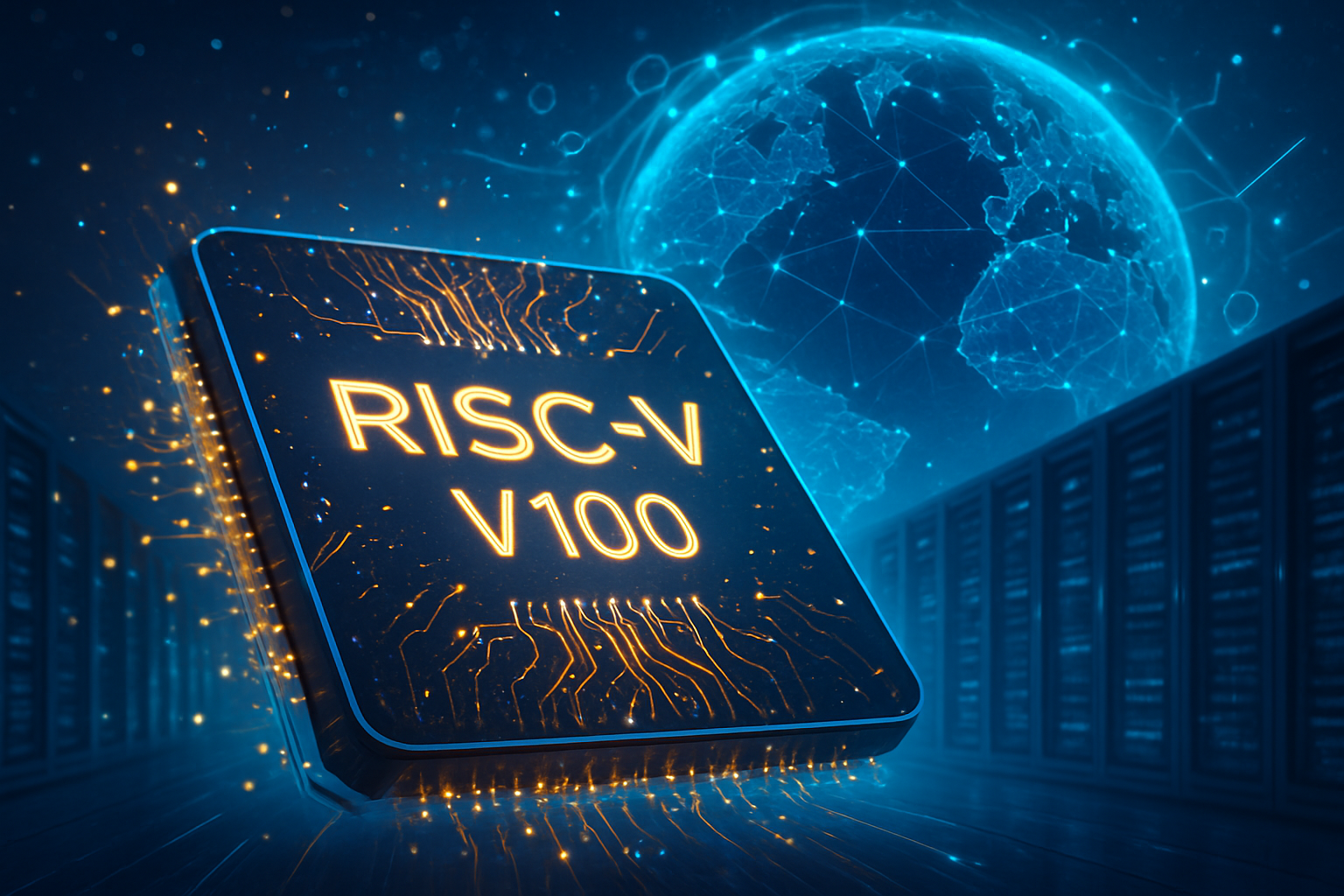
In a landmark moment for the global semiconductor industry, Taiwan Semiconductor Manufacturing Company (NYSE: TSM) has officially transitioned into high-volume manufacturing (HVM) for its 2-nanometer (N2) process technology as of January 2026. This milestone signals the dawn of the "Angstrom Era," moving beyond the limits of current 3nm nodes and providing the foundational hardware necessary to power the next generation of generative AI and hyperscale computing.
The transition to N2 represents more than just a reduction in size; it marks the most significant architectural shift for the foundry in over a decade. By moving from the traditional FinFET (Fin Field-Effect Transistor) structure to a sophisticated Nanosheet Gate-All-Around (GAAFET) design, TSMC has unlocked unprecedented levels of energy efficiency and performance. For the AI industry, which is currently grappling with skyrocketing energy demands in data centers, the arrival of 2nm silicon is being hailed as a critical lifeline for sustainable scaling.
Technical Mastery: The Shift to Nanosheet GAAFET
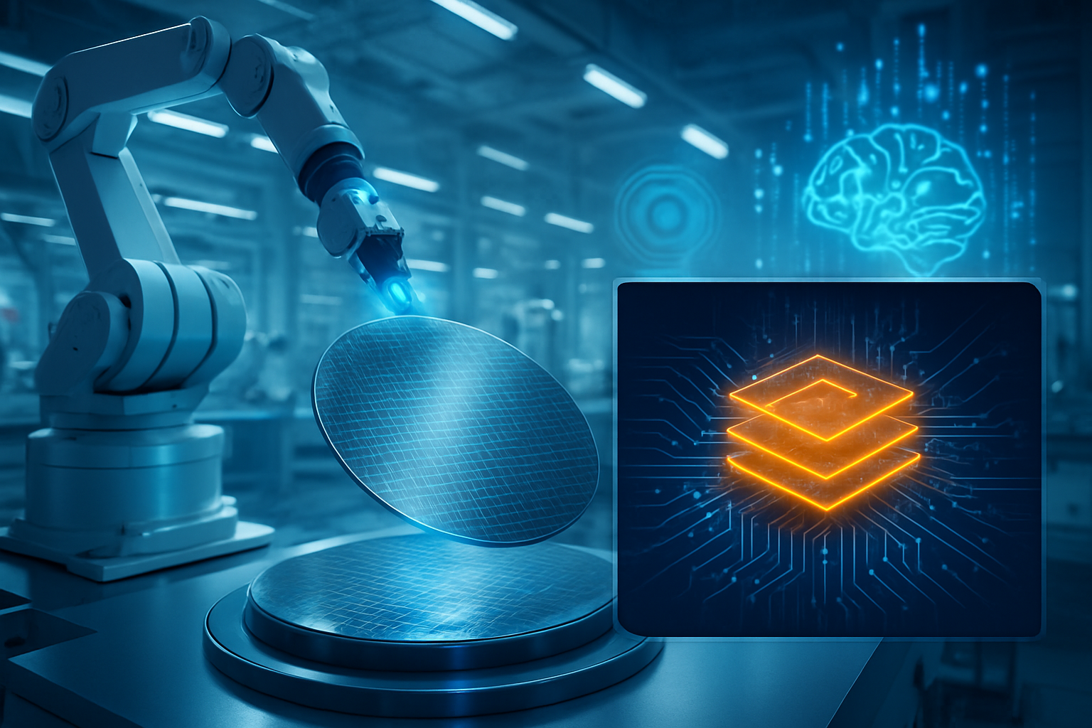
The technical core of the N2 node is the move to GAAFET architecture, where the gate wraps around all four sides of the channel (nanosheet). This differs from the FinFET design used since the 16nm era, which only covered three sides. The superior electrostatic control provided by GAAFET drastically reduces current leakage, a major hurdle in shrinking transistors further. TSMC’s implementation also features "NanoFlex" technology, allowing chip designers to adjust the width of individual nanosheets to prioritize either peak performance or ultra-low power consumption on a single die.
The specifications for the N2 process are formidable. Compared to the previous N3E (3nm) node, the 2nm process offers a 10% to 15% increase in speed at the same power level, or a substantial 25% to 30% reduction in power consumption at the same clock frequency. Furthermore, chip density has increased by approximately 1.15x. While the density jump is more iterative than previous "full-node" leaps, the efficiency gains are the real headline, especially for AI accelerators that run at high thermal envelopes. Early reports from the production lines in Taiwan suggest that TSMC has already cleared the "yield wall," with logic test chip yields stabilizing between 70% and 80%—a remarkably high figure for a new transistor architecture at this stage.
The Global Power Play: Impact on Tech Giants and Competitors
The primary beneficiaries of this HVM milestone are expected to be Apple (NASDAQ: AAPL) and NVIDIA (NASDAQ: NVDA). Apple, traditionally TSMC’s lead customer, is reportedly utilizing the N2 node for its upcoming A20 and M5 series chips, which will likely debut later this year. For NVIDIA, the transition to 2nm is vital for its next-generation AI GPU architectures, code-named "Rubin," which require massive throughput and efficiency to maintain dominance in the training and inference market. Other major players like Advanced Micro Devices (NASDAQ: AMD) and MediaTek are also in the queue to leverage the N2 capacity for their flagship 2026 products.
The competitive landscape is more intense than ever. Intel (NASDAQ: INTC) is currently ramping its 18A (1.8nm) node, which features its own "RibbonFET" and "PowerVia" backside power delivery. While Intel aims to challenge TSMC on performance, TSMC’s N2 retains a clear lead in transistor density and manufacturing maturity. Meanwhile, Samsung (KRX: 005930) continues to refine its SF2 process. Although Samsung was the first to adopt GAA at the 3nm stage, its yields have reportedly lagged behind TSMC’s, giving the Taiwanese giant a significant strategic advantage in securing the largest, most profitable contracts for the 2026-2027 product cycles.
A Crucial Turn in the AI Landscape
The arrival of 2nm HVM arrives at a pivotal moment for the AI industry. As large language models (LLMs) grow in complexity, the hardware bottleneck has shifted from raw compute to power efficiency and thermal management. The 30% power reduction offered by N2 will allow data center operators to pack more compute density into existing facilities without exceeding power grid limits. This shift is essential for the continued evolution of "Agentic AI" and real-time multimodal models that require constant, low-latency processing.
Beyond technical metrics, this milestone reinforces the geopolitical importance of the "Silicon Shield." Production is currently concentrated in TSMC’s Baoshan (Hsinchu) and Kaohsiung facilities. Baoshan, designated as the "mother fab" for 2nm, is already running at a capacity of 30,000 wafers per month, with the Kaohsiung facility rapidly scaling to meet overflow demand. This concentration of the world’s most advanced manufacturing capability in Taiwan continues to make the island the indispensable hub of the global digital economy, even as TSMC expands its international footprint in Arizona and Japan.
The Road Ahead: From N2 to the A16 Milestone
Looking forward, the N2 node is just the beginning of the Angstrom Era. TSMC has already laid out a roadmap that leads to the A16 (1.6nm) node, scheduled for high-volume manufacturing in late 2026. The A16 node will introduce the "Super Power Rail" (SPR), TSMC’s version of backside power delivery, which moves power routing to the rear of the wafer. This innovation is expected to provide an additional 10% boost in speed by reducing voltage drop and clearing space for signal routing on the front of the chip.
Experts predict that the next eighteen months will see a flurry of announcements as AI companies optimize their software to take advantage of the new 2nm hardware. Challenges remain, particularly regarding the escalating costs of EUV (Extreme Ultraviolet) lithography and the complex packaging required for "chiplet" designs. However, the successful HVM of N2 proves that Moore’s Law—while certainly becoming more expensive to maintain—is far from dead.
Summary: A New Foundation for Intelligence
TSMC’s successful launch of 2nm HVM marks a definitive transition into a new epoch of computing. By mastering the Nanosheet GAAFET architecture and scaling production at Baoshan and Kaohsiung, the company has secured its position at the apex of the semiconductor industry for the foreseeable future. The performance and efficiency gains provided by the N2 node will be the primary engine driving the next wave of AI breakthroughs, from more capable consumer devices to more efficient global data centers.
As we move through 2026, the focus will shift toward how quickly lead customers can integrate these chips into the market and how competitors like Intel and Samsung respond. For now, the "Angstrom Era" has officially arrived, and with it, the promise of a more powerful and energy-efficient future for artificial intelligence.
This content is intended for informational purposes only and represents analysis of current AI developments.
TokenRing AI delivers enterprise-grade solutions for multi-agent AI workflow orchestration, AI-powered development tools, and seamless remote collaboration platforms.
For more information, visit https://www.tokenring.ai/.