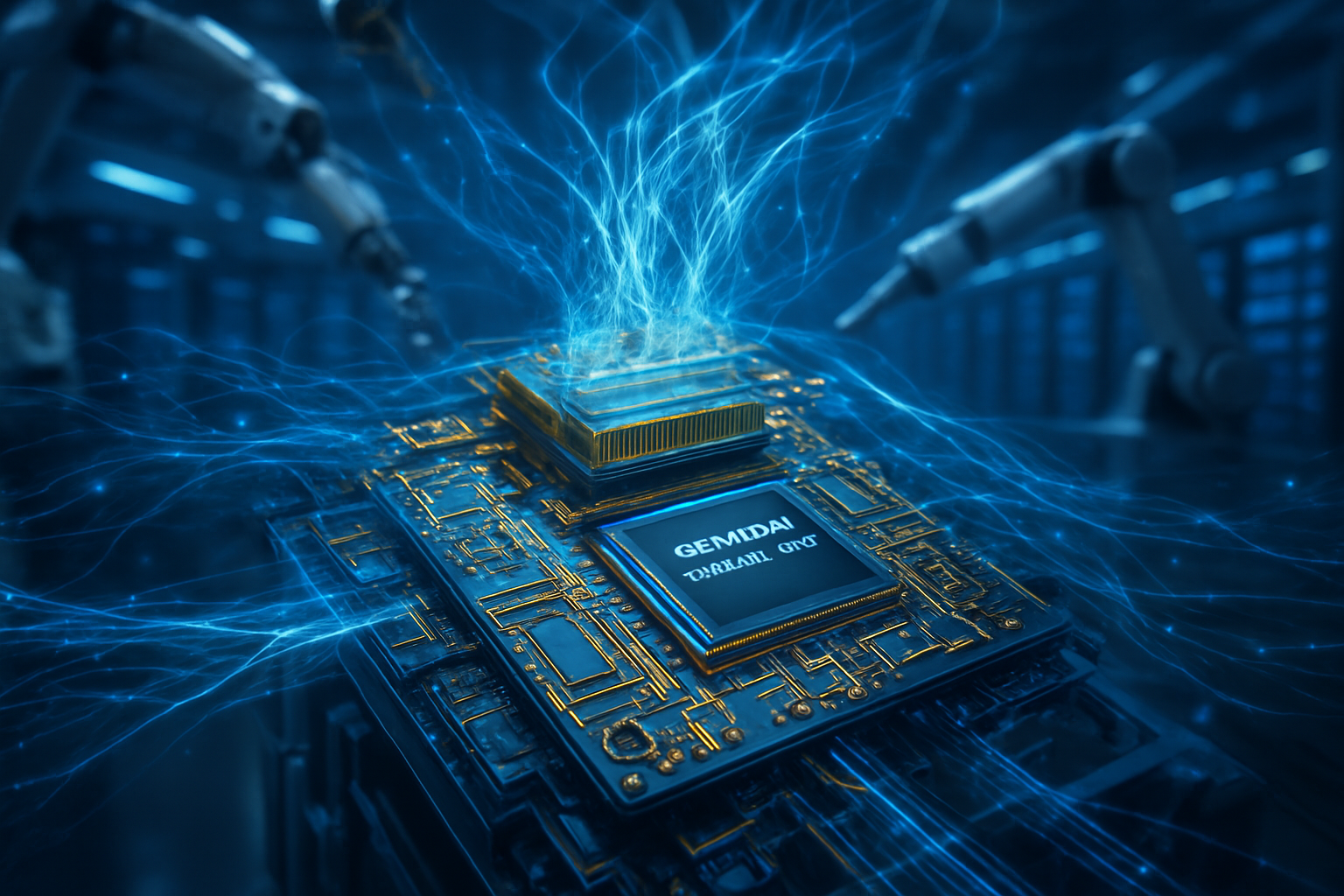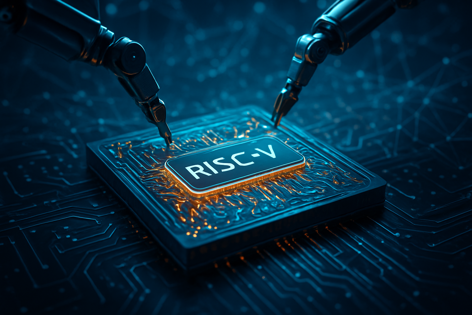
The semiconductor industry has officially entered a new epoch this month as the "Glass Substrate Age" transitions from a laboratory ambition to a commercial reality. At the heart of this revolution is Intel Corporation (Nasdaq: INTC), which has begun shipping its highly anticipated Xeon 6+ "Clearwater Forest" processors, the first high-volume chips to utilize a glass substrate core. Simultaneously, in Covington, Georgia, Absolics—a subsidiary of SKC Co. Ltd. (KRX: 011790)—has reached a pivotal milestone by commencing volume shipments of its specialized glass substrates to top-tier AI hardware partners, signaling the end of the 30-year dominance of organic materials in high-performance packaging.
This technological pivot is driven by the insatiable demands of generative AI, which has pushed traditional organic substrates to their physical breaking point. As AI "super-chips" grow larger and consume more power, they encounter a "warpage wall" where organic resins deform under heat, causing micro-cracks and signal failure. Glass, with its superior thermal stability and atomic-level flatness, provides the structural foundation necessary for the massive, multi-die packages required to train the next generation of Large Language Models (LLMs).
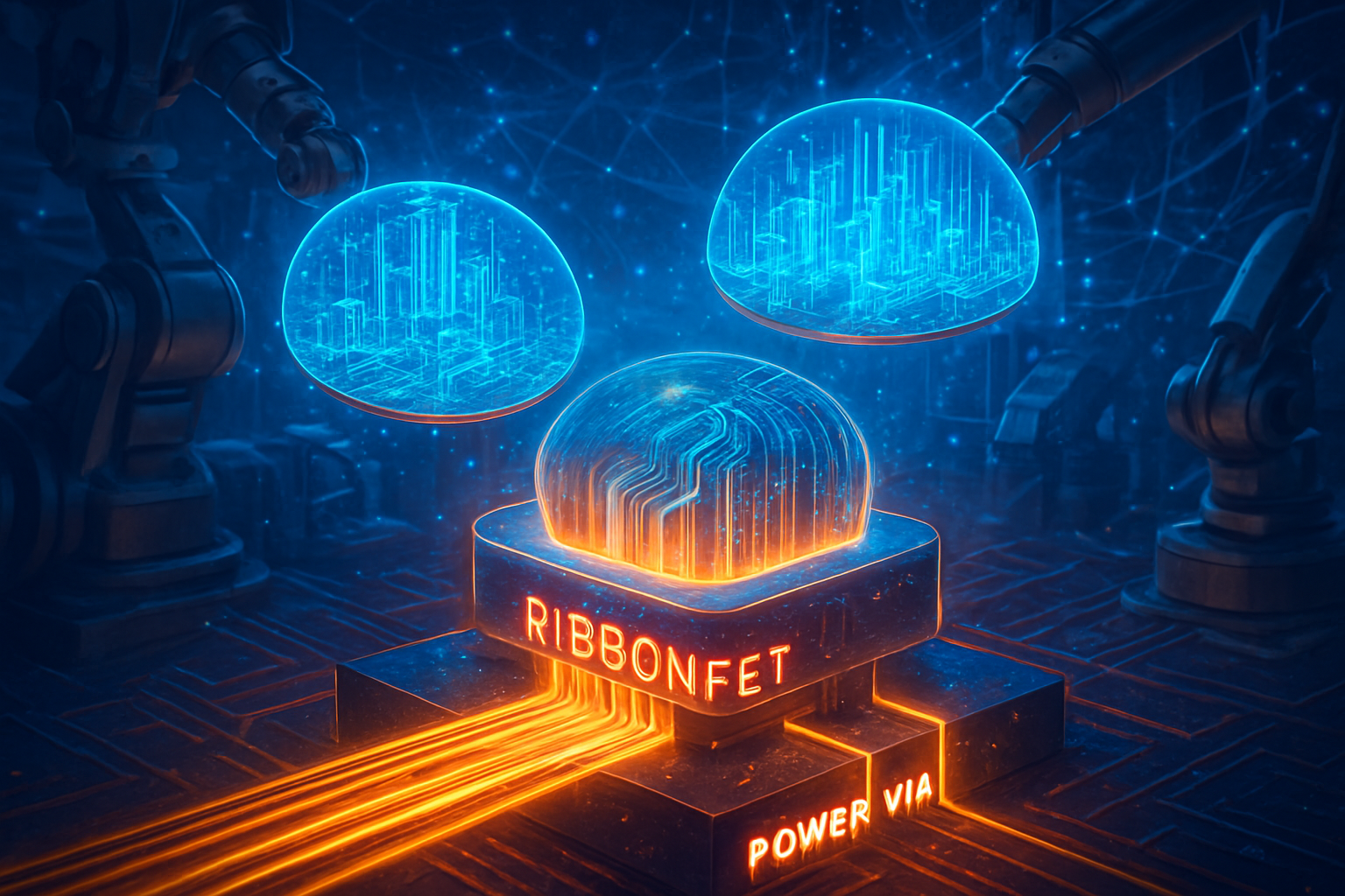
The Technical Leap: Clearwater Forest and the 10-2-10 Architecture
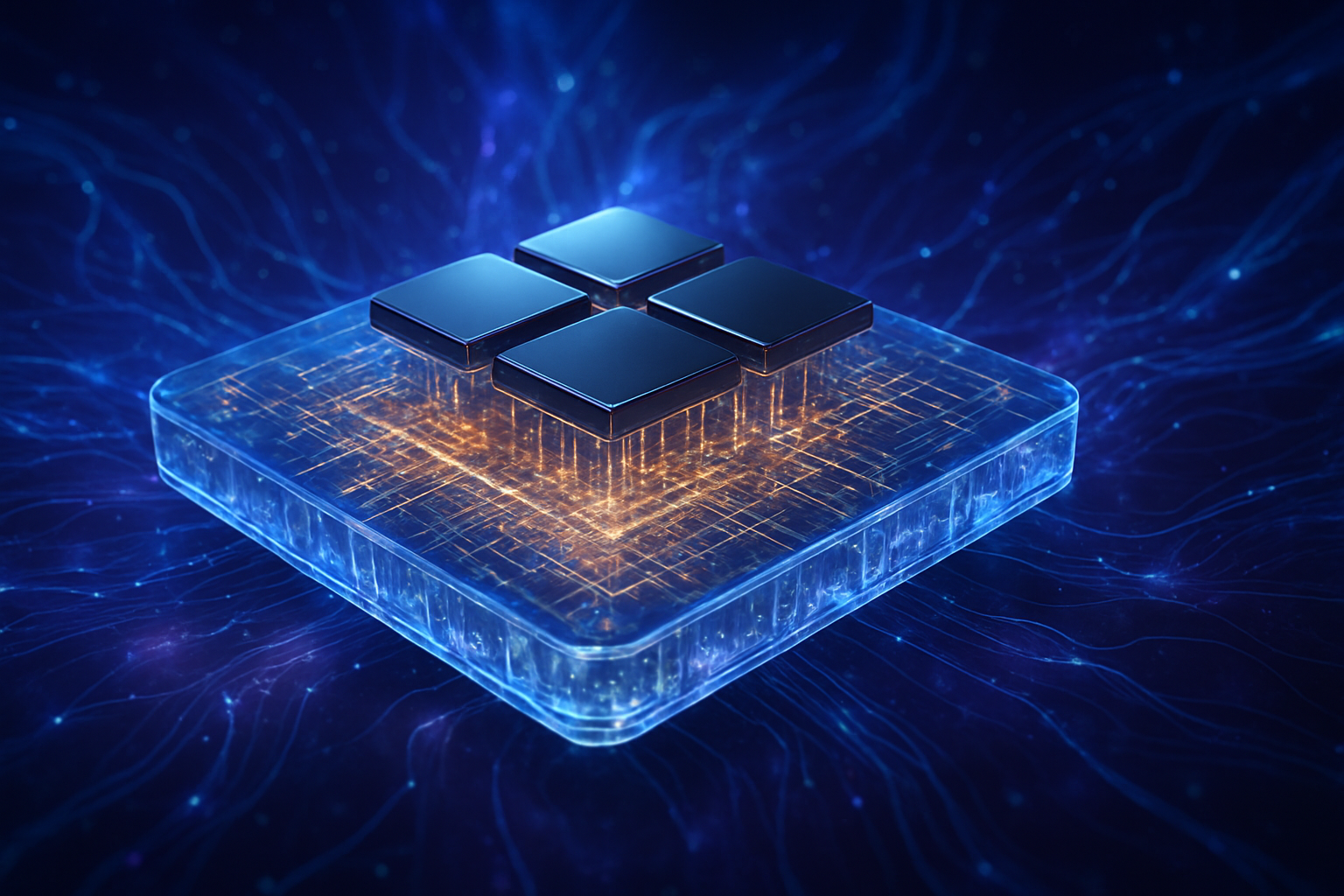
Intel’s Clearwater Forest is not just a showcase for the company’s Intel 18A process node; it is a masterclass in advanced packaging. Utilizing a "10-2-10" build-up configuration, the chip features a central 800-micrometer glass core sandwiched between 10 layers of high-density redistribution circuitry on either side. This glass core is critical because its Coefficient of Thermal Expansion (CTE) is nearly identical to that of silicon. When the 288 "Darkmont" E-cores within Clearwater Forest ramp up to peak power, the glass substrate expands at the same rate as the silicon dies, preventing the mechanical stress that plagued previous generations of organic-based server chips.
Beyond thermal stability, glass substrates enable a massive leap in interconnect density via Through-Glass Vias (TGVs). Unlike the mechanical or laser-drilled holes in organic substrates, TGVs are etched using high-precision semiconductor lithography, allowing for a 10x increase in vertical connections. This allows Intel to use its Foveros Direct 3D technology to bond compute tiles with sub-10-micrometer pitches, effectively turning a collection of discrete chiplets into a single, high-bandwidth "System-on-Package." The result is a 5x increase in L3 cache capacity and a 50% improvement in power delivery efficiency compared to the previous Sierra Forest generation.
Market Disruptions: Georgia’s "Silicon Peach" and the Competitive Scramble
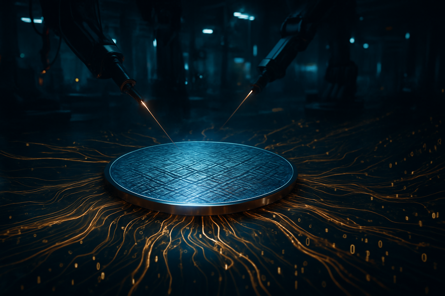
The arrival of the Glass Age is also reshaping the global supply chain. In Covington, Georgia, the $600 million Absolics facility—backed by strategic investor Applied Materials (Nasdaq: AMAT) and the U.S. CHIPS Act—has become the first dedicated "merchant" plant for glass substrates. As of January 2026, Absolics is reportedly shipping volume samples to Advanced Micro Devices (Nasdaq: AMD) for its upcoming MI400-series AI accelerators. By positioning itself as a neutral supplier, Absolics is challenging the vertically integrated dominance of Intel, offering other tech giants like Amazon (Nasdaq: AMZN) a path to adopt glass technology for their custom Graviton and Trainium chips.
The competitive implications are profound. While Taiwan Semiconductor Manufacturing Co. (NYSE: TSM) has long dominated the 2.5D packaging market with its CoWoS (Chip on Wafer on Substrate) technology, the shift to glass gives Intel a temporary "packaging lead" in the high-end server market. Samsung Electronics (KRX: 005930) has responded by accelerating its own glass substrate roadmap, targeting a 2027 launch, but the early mover advantage currently rests with the Intel-Absolics axis. For AI labs and cloud providers, this development means a new tier of hardware that can support "reticle-busting" package sizes—chips that are physically larger than what was previously possible—allowing for more HBM4 memory stacks to be packed around a single GPU or CPU.
Breaking the Warpage Wall: Why Glass is the New Silicon
The wider significance of this shift cannot be overstated. For decades, the industry relied on Ajinomoto Build-up Film (ABF), an organic resin, to host chips. However, as AI chips began to exceed 700W of power consumption, ABF-based substrates started to behave like "potato chips," warping and curving during the manufacturing process. Glass is fundamentally different; it maintains its structural integrity and near-perfect flatness even at temperatures up to 400°C. This allows for ultra-fine bump pitches (down to 45 micrometers and below) without the risk of "cold" solder joints, which are the leading cause of yield loss in massive AI packages.
Furthermore, glass is an exceptional electrical insulator. This reduces parasitic capacitance and signal loss, which are critical as data transfer speeds between chiplets approach terabit-per-second levels. By switching from organic materials to glass, chipmakers can reduce data transmission power requirements by up to 60%. This shift fits into a broader trend of "material innovation" in the AI era, where the industry is moving beyond simply shrinking transistors to rethinking the entire physical structure of the computer itself. It is a milestone comparable to the introduction of High-K Metal Gate technology or the transition to FinFET transistors.
The Horizon: From 2026 Ramps to 2030 Dominance
Looking ahead, the next 24 months will be focused on yield optimization and scaling. While glass is technically superior, it is also more fragile and currently more expensive to manufacture than traditional organic substrates. Experts predict that 2026 will be the year of "High-End Adoption," where glass is reserved for $20,000+ AI accelerators and flagship server CPUs. However, as Absolics begins its "Phase 2" expansion in Georgia—aiming to increase capacity from 12,000 to 72,000 square meters per year—economies of scale will likely bring glass technology into the high-end workstation and gaming markets by 2028.
Future applications extend beyond just CPUs and GPUs. The high-frequency performance of glass substrates makes them ideal for the upcoming 6G telecommunications infrastructure and integrated photonics, where light is used instead of electricity to move data between chips. The industry's long-term goal is "Optical I/O on Glass," a development that could theoretically increase chip-to-chip bandwidth by another 100x. The primary challenge remains the development of standardized handling equipment to prevent glass breakage during high-speed assembly, a hurdle that companies like Applied Materials are currently working to solve through specialized robotics and suction-based transport systems.
A Transparent Future for Artificial Intelligence
The launch of Intel’s Clearwater Forest and the operational ramp-up of the Absolics plant mark the definitive beginning of the Glass Substrate Age. This is not merely an incremental update to semiconductor packaging; it is a fundamental reconfiguration of the hardware foundation upon which modern AI is built. By solving the dual crises of thermal warpage and interconnect density, glass substrates have cleared the path for the multi-kilowatt "super-clusters" that will define the next decade of artificial intelligence development.
As we move through 2026, the industry will be watching two key metrics: the yield rates of Absolics' Georgia facility and the real-world performance of Intel’s 18A-based Clearwater Forest in hyperscale data centers. If these milestones meet expectations, the era of organic substrates will begin a rapid sunset, replaced by the clarity and precision of glass. For the AI industry, the "Glass Age" promises a future where the only limit to compute power is the speed of light itself.
This content is intended for informational purposes only and represents analysis of current AI developments.
TokenRing AI delivers enterprise-grade solutions for multi-agent AI workflow orchestration, AI-powered development tools, and seamless remote collaboration platforms.
For more information, visit https://www.tokenring.ai/.