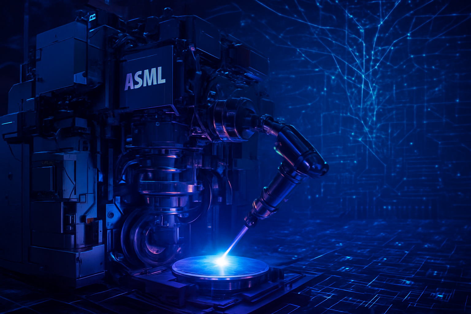
As of January 2026, the artificial intelligence revolution has hit a physical limit not defined by code or algorithms, but by the physical availability of High Bandwidth Memory (HBM). What was once a niche segment of the semiconductor market has transformed into the "currency of AI," with industry leaders SK Hynix (KRX: 000660) and Micron (NASDAQ: MU) officially announcing that their production lines are entirely sold out through the end of 2026. This unprecedented scarcity has triggered a global scramble among tech giants, turning the silicon supply chain into a high-stakes geopolitical battlefield where the ability to secure memory determines which companies will lead the next era of generative intelligence.
The immediate significance of this shortage cannot be overstated. As NVIDIA (NASDAQ: NVDA) transitions from its Blackwell architecture to the highly anticipated Rubin platform, the demand for next-generation HBM4 has decoupled from traditional market cycles. We are no longer witnessing a standard supply-and-demand fluctuation; instead, we are seeing the emergence of a structural "memory tax" on all high-end computing. With lead times for new orders effectively non-existent, the industry is bracing for a two-year period where the growth of AI model parameters may be capped not by innovation, but by the sheer volume of memory stacks available to feed the GPUs.
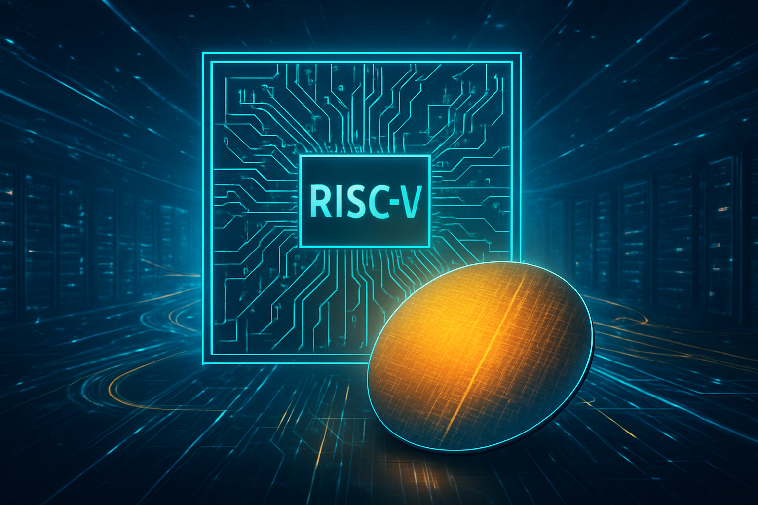
The Technical Leap to HBM4
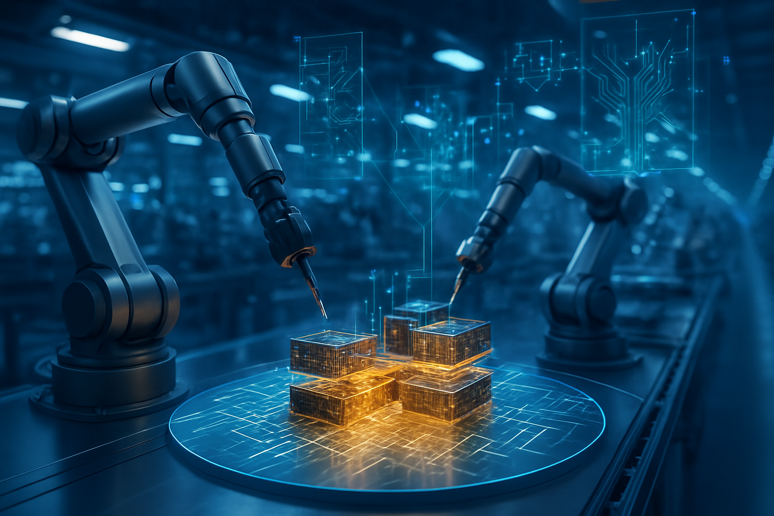
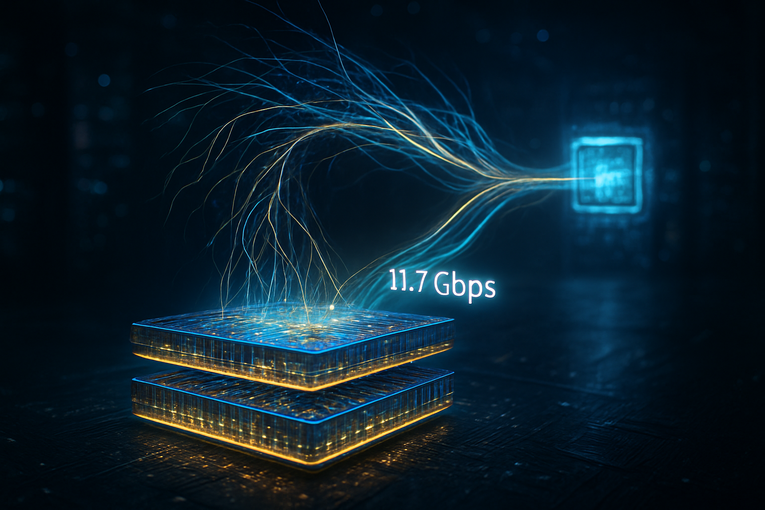
The transition from HBM3e to HBM4 represents the most significant architectural overhaul in the history of memory technology. While HBM3e served as the workhorse for the 2024–2025 AI boom, HBM4 is a fundamental redesign aimed at shattering the "Memory Wall"—the bottleneck where processor speed outpaces the rate at which data can be retrieved. The most striking technical leap in HBM4 is the doubling of the interface width from 1,024 bits per stack to a massive 2,048-bit bus. This allows for bandwidth speeds exceeding 2.0 TB/s per stack, a necessity for the massive "Mixture of Experts" (MoE) models that now dominate the enterprise AI landscape.
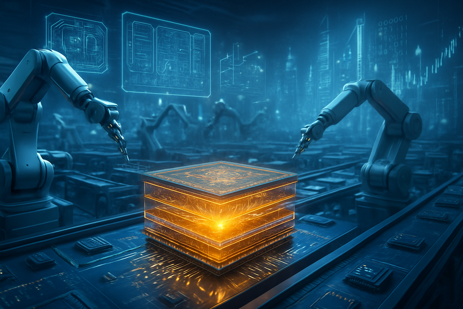
Unlike previous generations, HBM4 moves away from a pure memory manufacturing process for its "base die"—the foundation layer that communicates with the GPU. For the first time, memory manufacturers are collaborating with foundries like TSMC (NYSE: TSM) to build these base dies using advanced logic processes, such as 5nm or 12nm nodes. This integration allows for customized logic to be embedded directly into the memory stack, significantly reducing latency and power consumption. By offloading certain data-shuffling tasks to the memory itself, HBM4 enables AI accelerators to spend more cycles on actual computation rather than waiting for data packets to arrive.
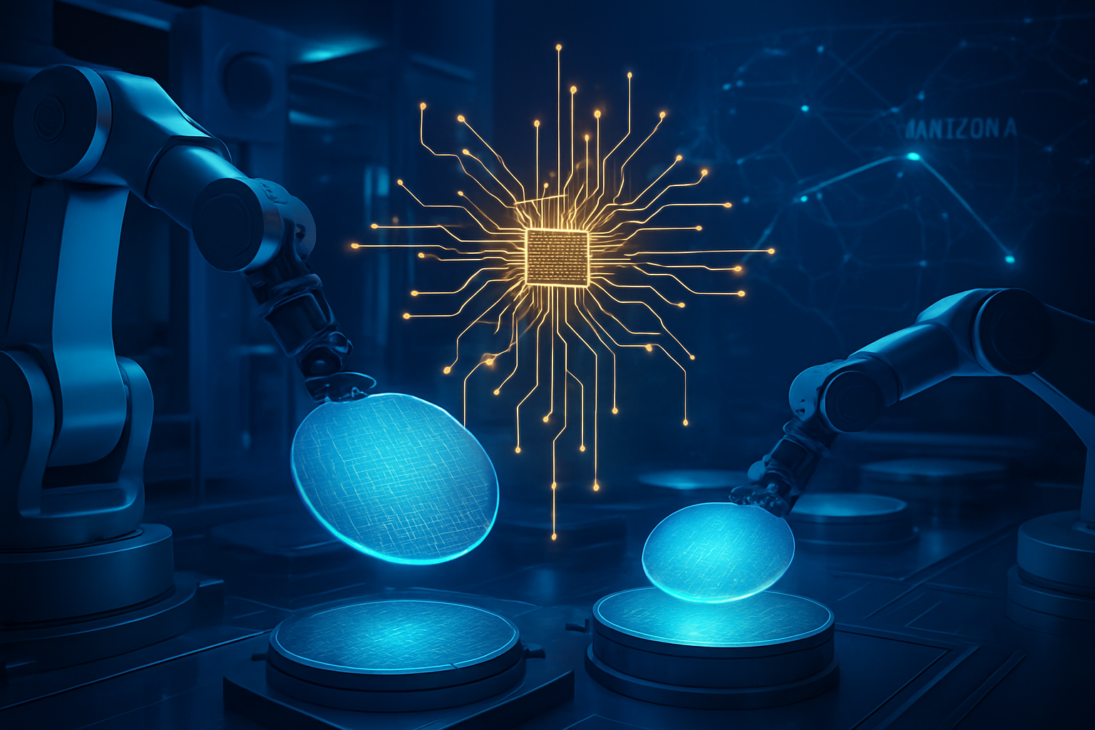
The initial reactions from the AI research community have been a mix of awe and anxiety. Experts at major labs note that while HBM4’s 12-layer and 16-layer configurations provide the necessary "vessel" for trillion-parameter models, the complexity of manufacturing these stacks is staggering. The industry is moving toward "hybrid bonding" techniques, which replace traditional microbumps with direct copper-to-copper connections. This is a delicate, low-yield process that explains why supply remains so constrained despite massive capital expenditures by the world’s big three memory makers.
Market Winners and Strategic Positioning
This scarcity creates a distinct "haves and have-nots" divide among technology giants. NVIDIA (NASDAQ: NVDA) remains the primary beneficiary of its early and aggressive securing of HBM capacity, effectively "cornering the market" for its upcoming Rubin GPUs. However, even the king of AI chips is feeling the squeeze, as it must balance its allocations between long-standing partners and the surging demand from sovereign AI projects. Meanwhile, competitors like Advanced Micro Devices (NASDAQ: AMD) and specialized AI chip startups find themselves in a precarious position, often forced to settle for previous-generation HBM3e or wait in a years-long queue for HBM4 allocations.
For tech giants like Google (NASDAQ: GOOGL) and Amazon (NASDAQ: AMZN), the shortage has accelerated the development of custom in-house silicon. By designing their own TPU and Trainium chips to work with specific memory configurations, these companies are attempting to bypass the generic market shortage. However, they remain tethered to the same handful of memory suppliers. The strategic advantage has shifted from who has the best algorithm to who has the most secure supply agreement with SK Hynix or Micron. This has led to a surge in "pre-payment" deals, where cloud providers are fronting billions of dollars in capital just to reserve production capacity for 2027 and beyond.
Samsung Electronics (KRX: 005930) is currently the "wild card" in this corporate chess match. After trailing SK Hynix in HBM3e yields for much of 2024 and 2025, Samsung has reportedly qualified its 12-stack HBM3e for major customers and is aggressively pivoting to HBM4. If Samsung can achieve stable yields on its HBM4 production line in 2026, it could potentially alleviate some market pressure. However, with SK Hynix and Micron already booked solid, Samsung’s capacity is being viewed as the last available "lifeboat" for companies that failed to secure early contracts.
The Global Implications of the $13 Billion Bet
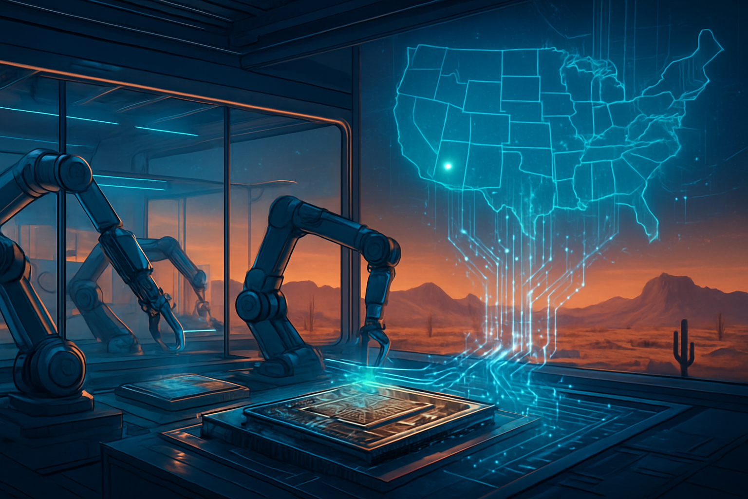
The broader significance of the HBM shortage lies in the physical realization that AI is not an ethereal cloud service, but a resource-intensive industrial product. The $13 billion investment by SK Hynix in its new "P&T7" advanced packaging facility in Cheongju, South Korea, signals a paradigm shift in the semiconductor industry. Packaging—the process of stacking and connecting chips—has traditionally been a lower-margin "back-end" activity. Today, it is the primary bottleneck. This $13 billion facility is essentially a fortress dedicated to the microscopic precision required to stack 16 layers of DRAM with near-zero failure rates.
This shift toward "advanced packaging" as the center of gravity for AI hardware has significant geopolitical and economic implications. We are seeing a massive concentration of critical infrastructure in a few specific geographic nodes, making the AI supply chain more fragile than ever. Furthermore, the "HBM tax" is spilling over into the consumer market. Because HBM production consumes three times the wafer capacity of standard DDR5 DRAM, manufacturers are reallocating their resources. This has caused a 60% surge in the price of standard RAM for PCs and servers over the last year, as the world's memory fabs prioritize the high-margin "currency of AI."
Comparatively, this milestone echoes the early days of the oil industry or the lithium rush for electric vehicles. HBM4 has become the essential fuel for the modern economy. Without it, the "Large Language Models" and "Agentic Workflows" that businesses now rely on would grind to a halt. The potential concern is that this "memory wall" could slow the pace of AI democratization, as only the wealthiest corporations and nations can afford to pay the premium required to jump the queue for these critical components.
Future Horizons: Beyond HBM4
Looking ahead, the road to 2027 will be defined by the transition to HBM4E (the "extended" version of HBM4) and the maturation of 3D integration. Experts predict that by 2027, the industry will move toward "Logic-DRAM 3D Integration," where the GPU and the HBM are not just side-by-side on a substrate but are stacked directly on top of one another. This would virtually eliminate data travel distance, but it presents monumental thermal challenges that have yet to be fully solved. If 2026 is the year of HBM4, 2027 will be the year the industry decides if it can handle the heat.
Near-term developments will focus on improving yields. Current estimates suggest that HBM4 yields are significantly lower than those of standard memory, often hovering between 40% and 60%. As SK Hynix and Micron refine their processes, we may see a slight easing of supply toward the end of 2026, though most analysts expect the "sold-out" status to persist as new AI applications—such as real-time video generation and autonomous robotics—require even larger memory pools. The challenge will be scaling production fast enough to meet the voracious appetite of the "AI Beast" without compromising the reliability of the chips.
Summary and Outlook
In summary, the HBM4 shortage of 2026 is the defining hardware story of the mid-2020s. The fact that the world’s leading memory producers are sold out through 2026 underscores the sheer scale of the AI infrastructure build-out. SK Hynix and Micron have successfully transitioned from being component suppliers to becoming the gatekeepers of the AI era, while the $13 billion investment in packaging facilities marks the beginning of a new chapter in semiconductor manufacturing where "stacking" is just as important as "shrinking."
As we move through the coming months, the industry will be watching Samsung’s yield rates and the first performance benchmarks of NVIDIA’s Rubin architecture. The significance of HBM4 in AI history will be recorded as the moment when the industry moved past pure compute power and began to solve the data movement problem at a massive, industrial scale. For now, the "currency of AI" remains the rarest and most valuable asset in the tech world, and the race to secure it shows no signs of slowing down.
This content is intended for informational purposes only and represents analysis of current AI developments.
TokenRing AI delivers enterprise-grade solutions for multi-agent AI workflow orchestration, AI-powered development tools, and seamless remote collaboration platforms.
For more information, visit https://www.tokenring.ai/.