The stranglehold that proprietary chip architectures have long held over the data center and edge computing markets is beginning to fracture. In a landmark move for the open-source hardware movement, SpacemiT has announced the launch of its Vital Stone V100, a server-class RISC-V processor designed specifically to handle the surging demands of the Edge AI era. This development, coupled with a massive $86 million Series B funding round for SpacemiT earlier this month, signals a paradigm shift in how artificial intelligence is being processed locally—moving away from the restrictive licensing of ARM Holdings (NASDAQ: ARM) and the power-hungry legacy of Intel (NASDAQ: INTC) and AMD (NASDAQ: AMD).
The significance of this announcement cannot be overstated. As of January 23, 2026, the industry is witnessing a "Great Migration" toward open-standard architectures. For years, RISC-V was relegated to low-power microcontrollers and simple IoT devices. However, SpacemiT’s jump into the server space, backed by the Beijing Artificial Intelligence Industry Investment Fund, demonstrates that RISC-V has matured into a formidable competitor capable of powering high-performance AI inference and dense cloud workloads. This shift is being driven by the urgent need for "AI Sovereignty" and cost-efficient scaling, as companies look to bypass the high margins and supply chain bottlenecks associated with closed ecosystems.
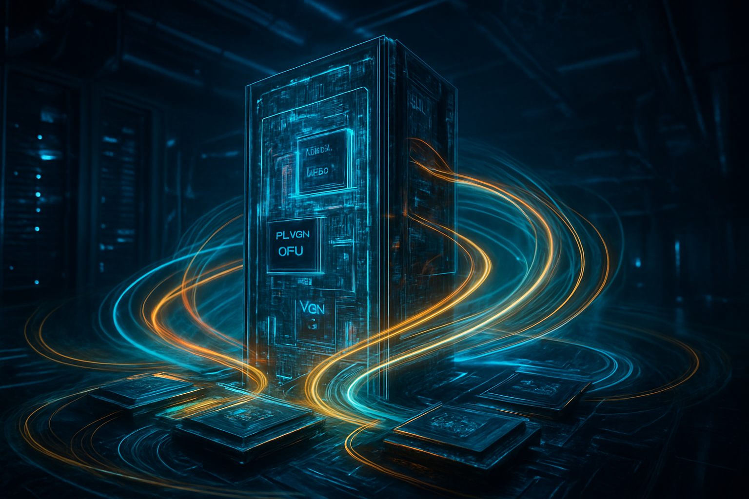
Technical Fusion: Inside the Vital Stone V100
At the heart of SpacemiT’s new offering is the X100 core, a high-performance RISC-V implementation that supports the RVA23 profile. The flagship Vital Stone V100 processor features a 64-core interconnect, marking a massive leap in density for the RISC-V ecosystem. Unlike traditional CPUs that rely on a separate Neural Processing Unit (NPU) for AI tasks, SpacemiT utilizes a "fusion" computing approach. It leverages the RISC-V Intelligence Matrix Extension (IME) and 256-bit Vector 1.0 capabilities to bake AI acceleration directly into the CPU's instruction set. This architecture allows the V100 to achieve over 8 TOPS of INT8 performance per 16-core cluster, optimized specifically for the transformer-based models that dominate modern Edge AI.
Technical experts have noted that while the V100 is manufactured on a mature 12nm process, its performance-per-watt is exceptionally competitive. Initial benchmarks suggest the X100 core offers a 30% performance advantage over the ARM Cortex-A55 in edge-specific scenarios. By focusing on parallelized AI inference rather than raw single-core clock speeds, SpacemiT has created a processor that excels in high-density environments where power efficiency is the primary constraint. Furthermore, the V100 includes full support for Hypervisor 1.0 and advanced virtualization (IOMMU, APLIC), making it a viable "drop-in" replacement for virtualized data center environments that were previously the exclusive domain of x86 or ARM Neoverse.
Market Disruption and the Influx of Capital
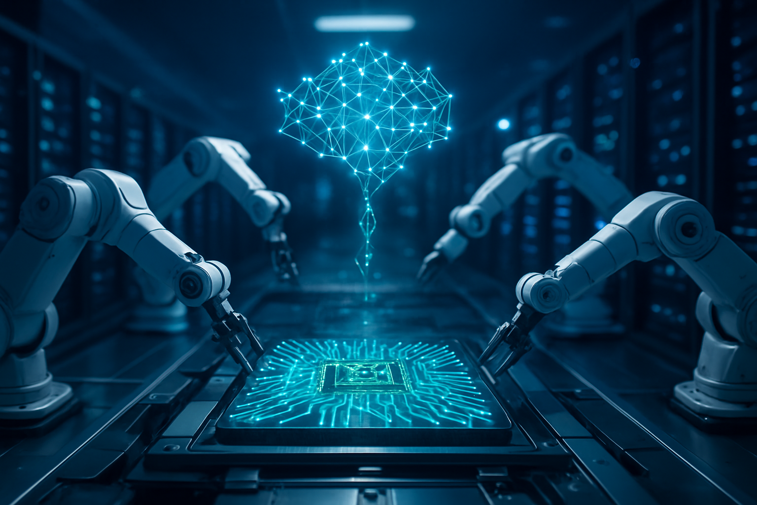
The rise of high-performance RISC-V is sending shockwaves through the semiconductor industry, forcing tech giants to re-evaluate their long-term hardware strategies. Meta Platforms (NASDAQ: META) recently signaled its commitment to this movement by completing the acquisition of RISC-V startup Rivos in late 2025. Meta is reportedly integrating Rivos' expertise into its internal Meta Training and Inference Accelerator (MTIA) program, aiming to reduce its multi-billion dollar reliance on NVIDIA (NASDAQ: NVDA) for internal inference tasks. Similarly, on January 15, 2026, SiFive announced a historic partnership with NVIDIA to integrate NVLink Fusion into its RISC-V silicon, allowing RISC-V CPUs to communicate directly with Hopper and Blackwell GPUs at native speeds.
This development poses a direct threat to ARM’s dominance in the data center "host CPU" market. For hyperscalers like Amazon (NASDAQ: AMZN) and its AWS Graviton program, the open nature of RISC-V allows for a level of customization that ARM’s licensing model does not permit. Companies can now strip away unnecessary legacy components of a chip to save on silicon area and power, a move that is expected to slash total cost of ownership (TCO) for AI-ready data centers by up to 25%. Startups are also benefiting from this influx of capital; Tenstorrent, led by industry legend Jim Keller, was recently valued at $2.6 billion following a massive funding round, positioning it as the premier provider of open-source AI hardware blocks.
Sovereignty and the New AI Landscape
The broader implications of the SpacemiT launch reflect a fundamental change in the global AI landscape: the transition from "AI in the Cloud" to "AI at the Edge." As local inference becomes the standard for privacy-sensitive applications—from autonomous vehicles to real-time healthcare monitoring—the demand for efficient, customizable hardware has outpaced the capabilities of general-purpose chips. RISC-V is uniquely suited for this trend because it allows developers to create bespoke accelerators for specific AI workloads without the "dead silicon" often found in multi-purpose x86 chips.
Furthermore, this expansion represents a critical milestone in the democratization of hardware. Historically, only a handful of companies had the capital to design and manufacture high-end server chips. By leveraging the open RISC-V standard, firms like SpacemiT are lowering the barrier to entry, potentially leading to a localized explosion of hardware innovation across the globe. However, this shift is not without its concerns. The geopolitical tension surrounding semiconductor production remains a factor, and the fragmentation of the RISC-V ecosystem—where different vendors might implement slightly different instruction set extensions—remains a potential hurdle for software developers trying to write code that runs everywhere.
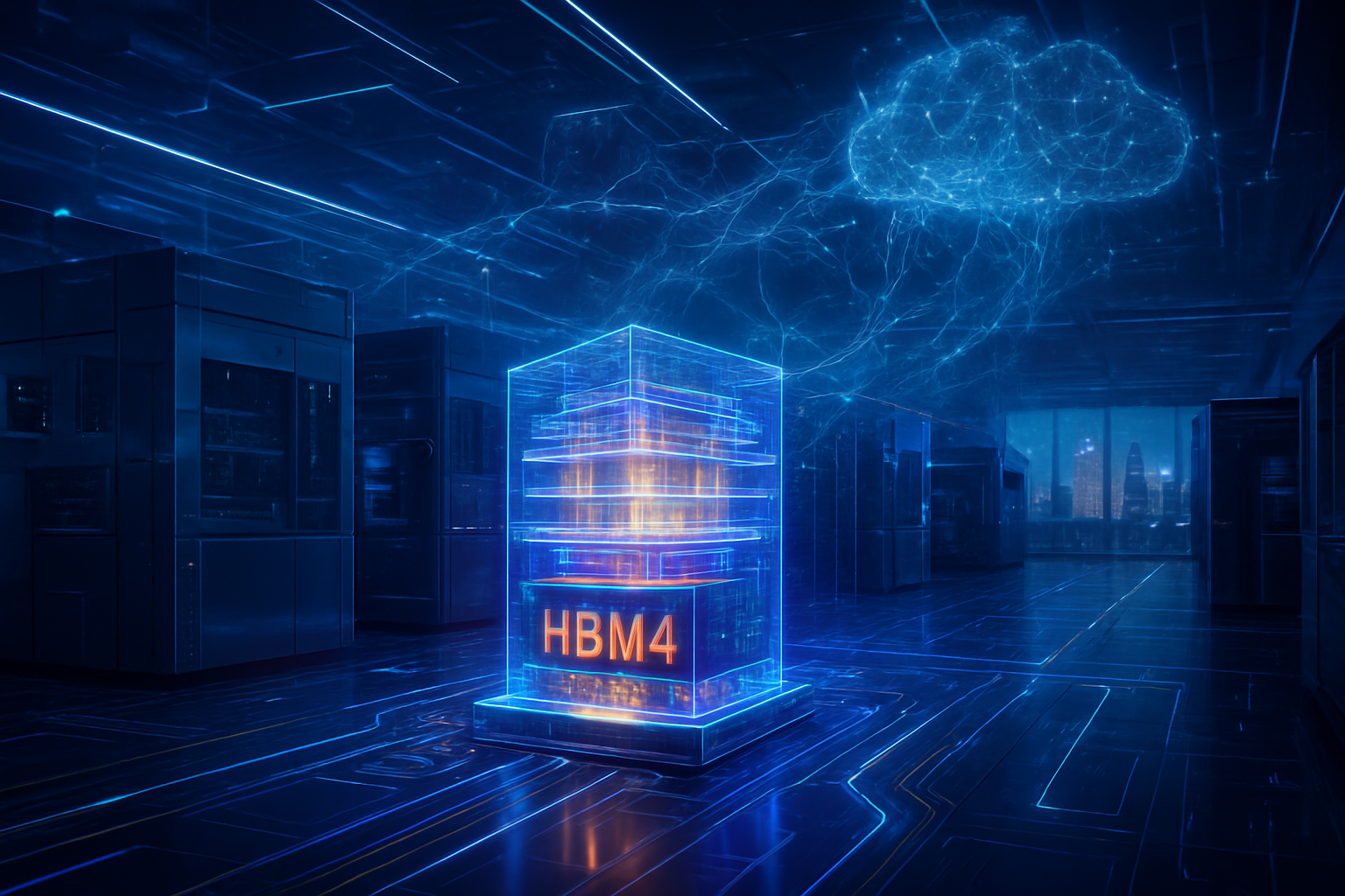
The Horizon: From Edge to Exascale
Looking ahead, the next 12 to 18 months will be defined by the "Software Readiness" phase of the RISC-V expansion. While the hardware specs of the Vital Stone V100 are impressive, the ultimate success of the platform will depend on how quickly the AI software stack—including frameworks like PyTorch and TensorFlow—is optimized for the RISC-V Intelligence Matrix Extension. SpacemiT has already confirmed that its K3 processor, an 8-to-16 core variant of the X100 core, will enter mass production in April 2026, targeting the high-end industrial and edge computing markets.
Experts predict that we will see a surge in "hybrid" deployments, where RISC-V chips act as highly efficient management and inference controllers alongside NVIDIA GPUs. Long-term, as the RISC-V ecosystem matures, we may see the first truly "open-source data centers" where every layer of the stack, from the instruction set architecture (ISA) to the operating system, is free from proprietary licensing. The challenge remains in scaling this technology to the 3nm and 2nm nodes, where the R&D costs are astronomical, but the capital influx into companies like Rivos and Tenstorrent suggests the industry is ready to make that bet.
A Watershed Moment for Open-Source Silicon
The launch of the SpacemiT Vital Stone V100 and the accompanying flood of venture capital into the RISC-V space mark the end of the "experimentation phase" for open-source hardware. As of early 2026, RISC-V has officially entered the server-class arena, providing a credible, efficient, and cost-effective alternative to the incumbents. The $86 million infusion into SpacemiT is just the latest indicator that investors believe the future of AI isn't just open software, but open hardware as well.
Key takeaways for the coming months include the scheduled April 2026 mass production of the K3 chip and the first small-scale deployments of the V100 in fourth-quarter 2026. This development is a watershed moment in AI history, proving that the collaborative model which revolutionized software via Linux is finally ready to do the same for the silicon that powers our world. Watch for more partnerships between RISC-V vendors and major cloud providers as they seek to hedge their bets against a volatile and expensive proprietary chip market.
This content is intended for informational purposes only and represents analysis of current AI developments.
TokenRing AI delivers enterprise-grade solutions for multi-agent AI workflow orchestration, AI-powered development tools, and seamless remote collaboration platforms.
For more information, visit https://www.tokenring.ai/.