As the artificial intelligence landscape shifts from software models to physical presence, the high-stakes collaboration between OpenAI and legendary former Apple (NASDAQ: AAPL) designer Jony Ive is finally coming into focus. Internally codenamed "Sweetpea," the project represents a radical departure from the glowing rectangles that have dominated personal technology for nearly two decades. By fusing Ive’s minimalist "calm technology" philosophy with OpenAI’s multimodal intelligence, the duo aims to redefine how humans interact with machines, moving away from the "app-and-tap" era toward a world of ambient, audio-first assistance.
The development is more than just a high-end accessory; it is a direct challenge to the smartphone's hegemony. With a targeted unveiling in the second half of 2026, OpenAI is positioning itself not just as a service provider but as a full-stack hardware titan. Supported by a massive capital injection from SoftBank (TYO: 9984) and a talent-rich acquisition of Ive’s secretive hardware startup, the "Sweetpea" project is the most credible attempt yet to create a "post-smartphone" interface.
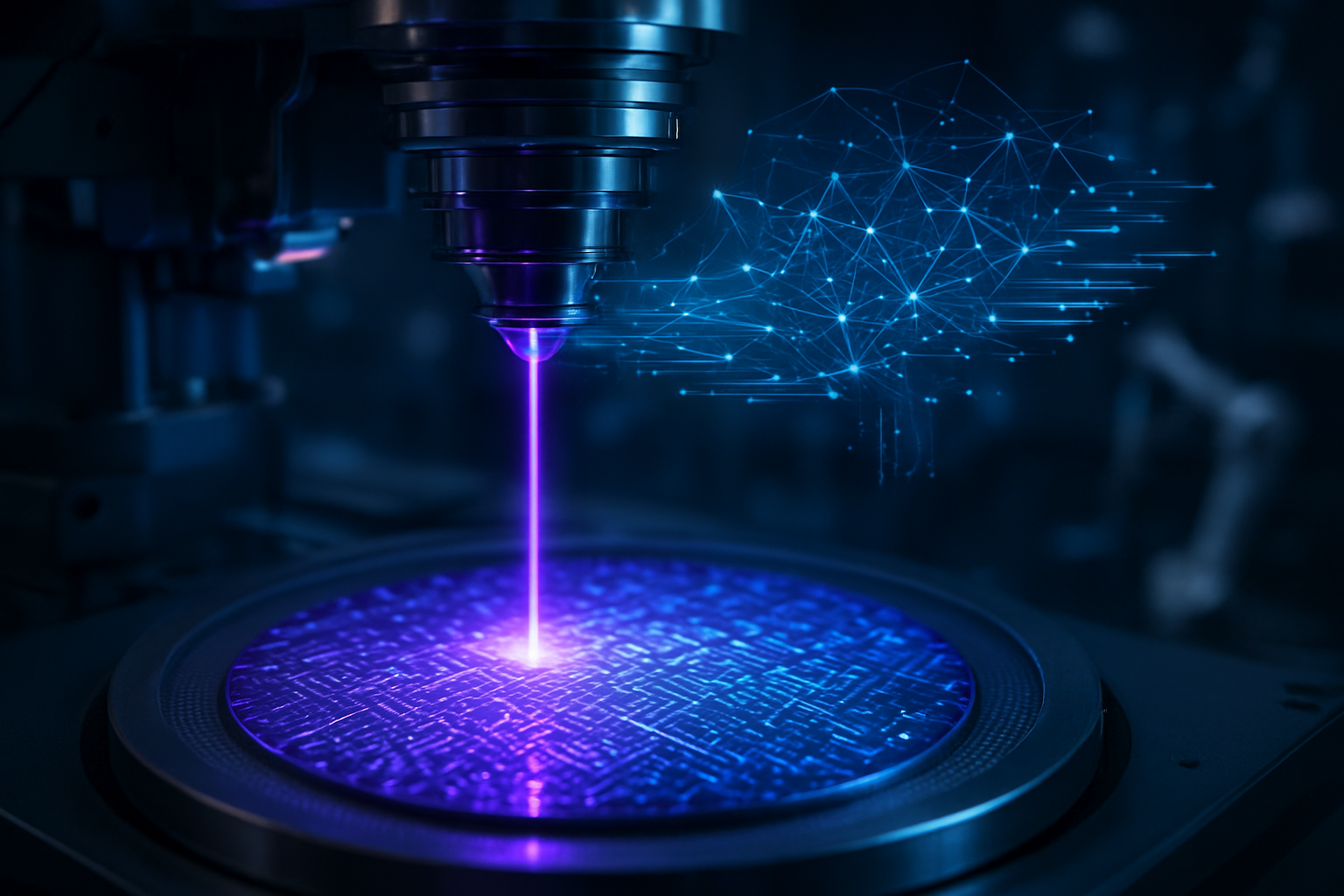
At the heart of the "Sweetpea" project is a design philosophy that rejects the blue-light addiction of traditional screens. The device is reported to be a screenless, audio-focused wearable with a unique "behind-the-ear" form factor. Unlike standard earbuds that fit inside the canal, "Sweetpea" features a polished, metal main unit—often described as a pebble or "eggstone"—that rests comfortably behind the ear. This design allows for a significantly larger battery and, more importantly, the integration of cutting-edge 2nm specialized chips capable of running high-performance AI models locally, reducing the latency typically associated with cloud-based assistants.
Technically, the device leverages OpenAI’s multimodal capabilities, specifically an evolution of GPT-4o, to act as a "sentient whisper." It uses a sophisticated array of microphones and potentially compact, low-power vision sensors to "see" and "hear" the user's environment in real-time. This differs from existing attempts like the Humane AI Pin or Rabbit R1 by focusing on ergonomics and "ambient presence"—the idea that the AI should be always available but never intrusive. Initial reactions from the AI research community are cautiously optimistic, with many praising the shift toward "proactive" AI that can anticipate needs based on environmental context, though concerns regarding "always-on" privacy remain a significant hurdle for public acceptance.
The implications for the tech industry are seismic. By developing its own hardware, OpenAI is attempting to bypass the "middleman" of the App Store and Google (NASDAQ: GOOGL) Play Store, creating an independent ecosystem where it owns the entire user journey. This move is seen as a "Code Red" for Apple (NASDAQ: AAPL), which has long dominated the high-end wearable market with its AirPods. If OpenAI can convince even a fraction of its hundreds of millions of ChatGPT users to adopt "Sweetpea," it could potentially siphon off trillions of "iPhone actions" that currently fuel Apple’s services revenue.
The project is fueled by a massive financial engine. In December 2025, SoftBank CEO Masayoshi Son reportedly finalized a $22.5 billion investment in OpenAI, specifically to bolster its hardware and infrastructure ambitions. Furthermore, OpenAI’s acquisition of Ive’s hardware startup, io Products, for a staggering $6.5 billion has brought over 50 elite Apple veterans—including former VP of Product Design Tang Tan—under OpenAI's roof. This consolidation of hardware expertise and AI dominance puts OpenAI in a unique strategic position, allowing it to compete with incumbents on both the silicon and design fronts simultaneously.
Broadly, "Sweetpea" fits into a larger industry trend toward ambient computing, where technology recedes into the background of daily life. For years, the tech world has searched for the "third core device" to sit alongside the laptop and the phone. While smartwatches and VR headsets have filled niches, "Sweetpea" aims for ubiquity. However, this transition is not without its risks. The failure of recent AI-focused gadgets has highlighted the "interaction friction" of voice-only systems; without a screen, users are forced to rely on verbal explanations, which can be slower and more socially awkward than a quick glance.
The project also raises profound questions about privacy and the nature of social interaction. An "always-on" device that constantly processes audio and visual data could face significant regulatory scrutiny, particularly in the European Union. Comparisons are already being drawn to the initial launch of the iPhone—a moment that fundamentally changed how humans relate to one another. If successful, "Sweetpea" could mark the transition from the era of "distraction" to the era of "augmentation," where AI acts as a digital layer over reality rather than a destination on a screen.
"Sweetpea" is only the beginning of OpenAI’s hardware ambitions. Internal roadmaps suggest that the company is planning a suite of five hardware devices by 2028, with "Sweetpea" serving as the flagship. Potential follow-ups include an AI-powered digital pen and a home-based smart hub, all designed to weave the OpenAI ecosystem into every facet of the physical world. The primary challenge moving forward will be scaling production; OpenAI has reportedly partnered with Foxconn (TPE: 2317) to manage the complex manufacturing required for its ambitious target of shipping 40 to 50 million units in its first year.
Experts predict that the success of the project will hinge on the software's ability to be truly "proactive." For a screenless device to succeed, the AI must be right nearly 100% of the time, as there is no visual interface to correct errors easily. As we approach the late-2026 launch window, the tech world will be watching for any signs of "GPT-5" or subsequent models that can handle the complex, real-world reasoning required for a truly useful audio-first companion.
In summary, the OpenAI/Jony Ive collaboration represents the most significant attempt to date to move the AI revolution out of the browser and into the physical world. Through the "Sweetpea" project, OpenAI is betting that Jony Ive's legendary design sensibilities can overcome the social and technical hurdles that have stymied previous AI hardware. With $22.5 billion in backing from SoftBank and a manufacturing partnership with Foxconn, the infrastructure is in place for a global-scale launch.
As we look toward the late-2026 release, the "Sweetpea" device will serve as a litmus test for the future of consumer technology. Will users be willing to trade their screens for a "sentient whisper," or is the smartphone too deeply ingrained in the human experience to be replaced? The answer will likely define the next decade of Silicon Valley and determine whether OpenAI can transition from a software pioneer to a generational hardware giant.
This content is intended for informational purposes only and represents analysis of current AI developments.
TokenRing AI delivers enterprise-grade solutions for multi-agent AI workflow orchestration, AI-powered development tools, and seamless remote collaboration platforms.
For more information, visit https://www.tokenring.ai/.