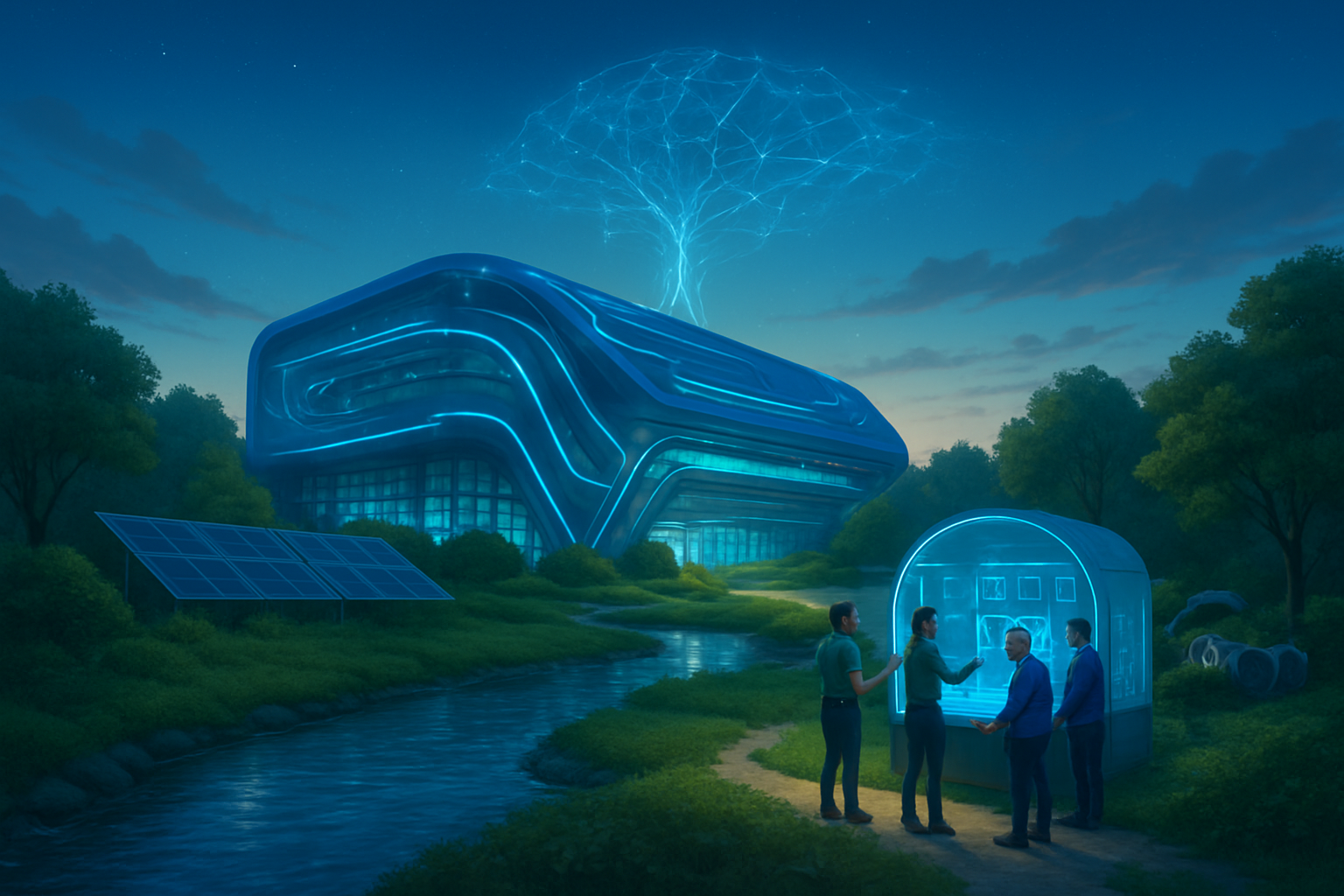
Tag: AI Infrastructure

  • Georgia’s AI Power Crisis: Lawmakers Introduce Landmark Statewide Data Center Ban to Save the Grid

    Georgia’s AI Power Crisis: Lawmakers Introduce Landmark Statewide Data Center Ban to Save the Grid

    The state of Georgia, once the fastest-growing hub for digital infrastructure in the Southeastern United States, has hit a dramatic legislative wall. In a move that has sent shockwaves through the technology and energy sectors, state lawmakers have introduced a landmark bill to implement the nation’s first comprehensive statewide moratorium on new data center construction. The legislation, House Bill 1012, introduced in early January 2026, marks a desperate attempt by state officials to decouple Georgia’s residential energy stability from the insatiable power demands of the generative artificial intelligence (AI) boom.

    This development signals a historic pivot in the relationship between state governments and the "hyperscale" tech giants that have flocked to the region. For years, Georgia lured companies with aggressive tax incentives and the promise of a robust grid. However, the sheer scale of the AI infrastructure required to power large language models has pushed the local utility, Southern Company (NYSE: SO), to its absolute limits. The immediate significance of this ban is a clear message to the industry: the era of "growth at any cost" has ended, and the physical constraints of the electrical grid now dictate the speed of digital innovation.

    The 10-Gigawatt Tipping Point: Technical and Legislative Drivers

    The move toward a moratorium was catalyzed by a series of technical and regulatory escalations throughout late 2025. In December, the Georgia Public Service Commission (PSC) approved an unprecedented request from Georgia Power, a subsidiary of Southern Company (NYSE: SO), to add an astronomical 10,000 megawatts (10 GW) of new energy capacity to the state’s grid. This expansion—enough to power over 8 million homes—was explicitly requested to meet the projected load from data centers, which now account for approximately 80% of all new electricity demand in the state.

    HB 1012 seeks to halt all new data center project approvals until March 1, 2027. This "cooling-off period" is designed to allow the newly formed Special Committee on Data Center Energy Planning to conduct a thorough audit of the state’s water and energy resources. Unlike previous attempts to limit the industry, such as the vetoed HB 1192 in 2024, the 2026 legislation focuses on "grid sovereignty." It mandates that any future data center over 100MW must undergo a rigorous "Conditional Certification" process, requiring up-front financial collateral to ensure that if the AI market cools, residential ratepayers aren't left paying for billions of dollars in stranded fossil-fuel infrastructure.

    Industry experts and the AI research community have expressed alarm at the technical bottleneck this creates. While the 2024-2025 period saw record deployments of the H100 and Blackwell chips from Nvidia Corporation (NASDAQ: NVDA), the actual physical deployment of these clusters is now being throttled not by chip shortages, but by the availability of high-voltage transformers and transmission lines. Researchers argue that without massive, centralized clusters in hubs like Atlanta, the training of "Frontier Models" expected in late 2026 could be delayed or fragmented, leading to higher latency and increased operational costs.

    Capital Flight and the Tech Giant Re-evaluation

    The legislative freeze poses an immediate strategic challenge for the world’s largest technology companies. Microsoft Corporation (NASDAQ: MSFT), Alphabet Inc. (NASDAQ: GOOGL), and Meta Platforms, Inc. (NASDAQ: META) have all invested billions into the "Silicon Peach" corridor, with massive campuses in Douglasville, Lithia Springs, and downtown Atlanta. The ban effectively halts several "Phase 2" expansions that were slated to break ground in mid-2026. For these companies, the uncertainty in Georgia may trigger a "capital flight" to states like Texas or Iowa, where energy markets are more deregulated, though even those regions are beginning to show signs of similar grid fatigue.

    The competitive implications are stark. Major AI labs like OpenAI and Anthropic rely on the massive infrastructure provided by Amazon.com, Inc. (NASDAQ: AMZN) and Microsoft to maintain their lead in the global AI race. If a primary hub like Georgia goes dark for new projects, it forces these giants into a more expensive, decentralized strategy. Market analysts suggest that companies with the most diversified geographic footprints will gain a strategic advantage, while those heavily concentrated in the Southeast may see their infrastructure costs spike as they are forced to compete for a dwindling supply of "pre-approved" power capacity.

    Furthermore, the ban threatens the burgeoning ecosystem of AI startups that rely on local low-latency "edge" computing. By halting construction, Georgia may inadvertently push its tech talent toward other regions, reversing years of progress in making Atlanta a premier technology destination. The disruption is not just to the data centers themselves, but to the entire supply chain, from construction firms specializing in advanced liquid cooling to local clean-energy developers who had planned projects around data center demand.

    A National Trend: The End of Data Center Exceptionalism

    Georgia is not an isolated case; it is the vanguard of a national trend toward "Data Center Accountability." In early 2026, similar moratoriums were proposed in Oklahoma and Maryland, while South Carolina is weighing a "Energy Independence" mandate that would require data centers to generate 100% of their power on-site. This fits into a broader global landscape where the environmental and social costs of AI are becoming impossible to ignore. For the first time, the "cloud" is being viewed not as a nebulous digital service, but as a heavy industrial neighbor that consumes vast amounts of water and requires the reopening of retired coal plants.

    The environmental impact has become a focal point of public concern. To meet the 10GW demand approved in December 2025, Georgia Power delayed the retirement of several coal units and proposed five new natural gas plants. This shift back toward fossil fuels to power "green" AI initiatives has sparked a backlash from environmental groups and residents who are seeing their utility bills rise to subsidize the expansion. The Georgia ban is a manifestation of this tension: a choice between meeting international AI milestones and maintaining local environmental standards.

    Comparatively, this moment mirrors the early 20th-century regulation of the railroad and telecommunications industries. Just as those technologies eventually faced "common carrier" laws and strict geographic oversight, AI infrastructure is losing its "exceptionalism." The transition from the "lure and subsidize" phase to the "regulate and restrict" phase is now in full swing, marking 2026 as the year the physical world finally pushed back against the digital expansion.

    Future Developments: SMRs and the Rise of the "Prosumer" Data Center

    Looking ahead, experts predict that the Georgia ban will force a radical evolution in how data centers are designed. With connection to the public grid becoming a legislative liability, the next generation of AI infrastructure will likely move toward "off-grid" or "behind-the-meter" solutions. This includes the accelerated deployment of Small Modular Reactors (SMRs) and on-site hydrogen fuel cells. Companies like Microsoft have already signaled interest in nuclear-powered data centers, and the Georgia moratorium could make these high-capital projects the only viable path forward for large-scale AI.

    In the near term, we can expect a fierce legal battle. Tech trade groups and industrial lobbyists are already preparing to challenge HB 1012, arguing that it violates interstate commerce and undermines national security by slowing domestic AI development. However, if the legislation holds, it will likely serve as a blueprint for other states facing similar grid instability. The long-term challenge will be the development of "grid-aware" AI, where training workloads are dynamically shifted to regions with excess renewable energy, rather than being anchored to a single, overloaded location.

    Predictions for the remainder of 2026 suggest that while construction may slow in Georgia, the demand for AI will not. This will lead to a surge in "infrastructure arbitrage," where companies pay a premium for existing, grandfathered capacity. We may also see the emergence of the "Prosumer" data center—facilities that not only consume power but also act as giant batteries for the grid, providing storage and stabilization services to justify their massive footprint to local regulators.

    A New Chapter in the AI Era

    The introduction of Georgia’s data center moratorium marks a definitive end to the first phase of the AI revolution. The key takeaways are clear: energy is the new silicon. The ability to secure gigawatts of power is now a more significant competitive advantage than the ability to design a new neural architecture. This development will likely be remembered as the moment the AI industry was forced to reconcile its digital ambitions with the physical realities of 20th-century infrastructure.

    As we move through the early months of 2026, the tech industry will be watching the Georgia General Assembly with intense scrutiny. The outcome of HB 1012 will determine whether the "Silicon Peach" remains a tech leader or becomes a cautionary tale of overextension. For now, the focus shifts from algorithms to transformers, and from software to sovereignty, as the state seeks to protect its citizens from the very technology it once sought to champion.


    This content is intended for informational purposes only and represents analysis of current AI developments.

    TokenRing AI delivers enterprise-grade solutions for multi-agent AI workflow orchestration, AI-powered development tools, and seamless remote collaboration platforms.
    For more information, visit https://www.tokenring.ai/.

  • Powering the AI Revolution: Brookfield’s Record-Breaking $10 Billion Green Energy “Super-Deal” with Microsoft and Google

    Powering the AI Revolution: Brookfield’s Record-Breaking $10 Billion Green Energy “Super-Deal” with Microsoft and Google

    In a move that fundamentally redefines the relationship between Big Tech and the global energy grid, Brookfield Renewable Partners (NYSE: BEP) has entered into a series of unprecedented framework agreements to power the next generation of artificial intelligence. Headlining this green energy "land grab" is a massive 10.5-gigawatt (GW) deal with Microsoft Corp. (NASDAQ: MSFT), complemented by a multi-gigawatt hydropower expansion for Alphabet Inc. (NASDAQ: GOOGL). Valued at over $10 billion, this represents the largest corporate clean energy procurement in history, signaling that the bottleneck for AI supremacy has shifted from silicon chips to raw electrical power.

    As of January 2026, the first contracts under these framework agreements are officially coming online, delivering carbon-free electricity to data centers across the United States and Europe. The scale is staggering: 10.5 GW is enough to power roughly 8 million homes or, more pivotally, to run dozens of the world’s most advanced AI training clusters. By securing this capacity through 2030, the tech giants are attempting to "future-proof" their AI ambitions against a backdrop of increasing grid instability and skyrocketing energy demand.

    The 10.5 GW Framework: A New Blueprint for Infrastructure

    The cornerstone of this development is the "Global Renewable Energy Framework Agreement" between Microsoft and Brookfield. Unlike traditional Power Purchase Agreements (PPAs), which typically focus on a single wind or solar farm, this framework provides a rolling pipeline of capacity to be delivered between 2026 and 2030. This ensures that as Microsoft scales its Azure AI infrastructure, the power is already accounted for, bypassing the years-long "interconnection queues" that currently plague the U.S. power grid.

    Technically, the deal spans a diverse portfolio of assets, including onshore wind, utility-scale solar, and—increasingly—advanced "firm" power sources. To meet the 24/7 "always-on" requirements of AI workloads, Brookfield is leveraging its massive hydroelectric fleet. In early 2026, Google also began receiving its first deliveries from a separate 3 GW hydropower framework with Brookfield, specifically targeting the PJM Interconnection grid—the densest data center region in the world. This focus on "baseload" renewables is a critical evolution from earlier strategies that relied solely on intermittent solar and wind, which often required carbon-heavy backups when the sun went down.

    Industry experts note that this deal is more than a simple purchase; it is a co-investment in the grid's modernization. The agreement includes provisions for "impactful carbon-free energy generation technologies," which analysts believe could eventually include long-duration battery storage and even small modular reactors (SMRs). The sheer volume of the investment—estimated between $10 billion and $11.5 billion for the Microsoft portion alone—provides Brookfield with the capital certainty to break ground on massive projects that would otherwise be deemed too risky for the merchant power market.

    The Hyperscaler Arms Race: Who Benefits and Who is Left Behind?

    The competitive implications of this deal are profound. By locking up 10.5 GW of Brookfield’s pipeline, Microsoft has effectively performed a "pre-emptive strike" on the renewable energy market. As AI models grow in complexity, the demand for power is expected to triple by 2030. Companies like Amazon.com Inc. (NASDAQ: AMZN) and Meta Platforms Inc. (NASDAQ: META) are now finding themselves in a fierce bidding war for the remaining "shovel-ready" renewable projects, potentially driving up the cost of green energy for non-tech industries.

    Brookfield Renewable stands as the primary beneficiary of this trend, transitioning from a utility operator to a critical partner in the global AI supply chain. The deal has solidified Brookfield’s position as the world's largest developer of pure-play renewable power, with a total pipeline that now exceeds 200 GW. For Google and Microsoft, these deals are strategic shields against the "power bottleneck." By vertically integrating their energy supply chains, they reduce their exposure to volatile spot-market electricity prices and ensure their AI services—from Gemini to Copilot—can remain operational even as the grid reaches its limits.

    However, the "crowding out" effect is a growing concern for smaller AI startups and traditional enterprises. As hyperscalers secure the vast majority of new renewable capacity, smaller players may be forced to rely on aging, fossil-fuel-dependent grids, potentially jeopardizing their ESG (Environmental, Social, and Governance) targets or facing higher operational costs that make their AI products less competitive.

    AI’s Energy Hunger and the Global Significance

    This $10 billion+ investment underscores a sobering reality: the AI revolution is an industrial-scale energy event. A single query to a generative AI model can consume ten times the electricity of a standard Google search. When multiplied by billions of users and the training of massive models like GPT-5 or Gemini 2, the energy requirements are astronomical. This deal marks the moment the tech industry moved beyond "carbon offsets" to "direct physical delivery" of green energy.

    The broader significance lies in how this fits into the global energy transition. Critics have long argued that AI would derail climate goals by keeping coal and gas plants online to meet surging demand. The Brookfield deal provides a counter-narrative, suggesting that the massive capital of Big Tech can be the primary catalyst for the largest green infrastructure build-out in human history. It mirrors the 19th-century railway boom, where private capital built the foundational infrastructure that eventually benefited the entire economy.

    There are, however, potential concerns. Grid operators are increasingly worried about the "data center density" in regions like Northern Virginia and Dublin. By injecting over 10 GW of demand into specific nodes, Microsoft and Google are testing the physical limits of high-voltage transmission lines. While the energy is "clean," the sheer volume of power moving through the system requires a complete overhaul of the physical wires and transformers that define the modern world.

    The Road Ahead: 24/7 Carbon-Free Energy and Beyond

    Looking toward the late 2020s, the "framework model" pioneered by Brookfield and Microsoft is expected to become the industry standard. We are likely to see similar multi-gigawatt deals announced involving advanced nuclear energy and deep-earth geothermal projects. In fact, the Global AI Infrastructure Investment Partnership (GAIIP)—a coalition including Microsoft, Nvidia Corp. (NASDAQ: NVDA), and BlackRock—is already aiming to mobilize $100 billion to expand this infrastructure even further.

    The next frontier for these deals will be "temporal matching," where every kilowatt-hour consumed by a data center is matched in real-time by a carbon-free source. This will necessitate a massive expansion in long-duration energy storage (LDES). Experts predict that by 2028, the "Big Three" hyperscalers will likely own more power generation capacity than many mid-sized nations, effectively operating as private utilities that happen to provide cloud services on the side.

    Wrapping Up: A Landmark in AI History

    The 10.5 GW Brookfield deal is a watershed moment that proves the AI boom is as much about physical infrastructure as it is about software. It represents a $10 billion bet that the clean energy transition can keep pace with the exponential growth of artificial intelligence.

    Key takeaways include:

    • Infrastructure is King: AI scaling is now limited by energy and cooling, not just GPUs.
    • Scale Matters: The shift from individual projects to multi-gigawatt "frameworks" allows for faster deployment of capital and cleaner energy.
    • Strategic Advantage: Microsoft and Google are using their balance sheets to secure a competitive edge in power, which may become the most valuable commodity of the 21st century.

    As we move through 2026, the industry will be watching the "interconnection speed"—how fast Brookfield can actually build these projects to match the blistering pace of AI hardware cycles. The success of this deal will determine whether the AI revolution will be remembered as a green industrial renaissance or a strain on the world’s most critical resource.


    This content is intended for informational purposes only and represents analysis of current AI developments.

    TokenRing AI delivers enterprise-grade solutions for multi-agent AI workflow orchestration, AI-powered development tools, and seamless remote collaboration platforms.
    For more information, visit https://www.tokenring.ai/.

  • The 10-Gigawatt Giga-Project: Inside the $500 Billion ‘Project Stargate’ Reshaping the Path to AGI

    The 10-Gigawatt Giga-Project: Inside the $500 Billion ‘Project Stargate’ Reshaping the Path to AGI

    In a move that has fundamentally rewritten the economics of the silicon age, OpenAI, SoftBank Group Corp. (TYO: 9984), and Oracle Corp. (NYSE: ORCL) have solidified their alliance under "Project Stargate"—a breathtaking $500 billion infrastructure initiative designed to build the world’s first 10-gigawatt "AI factory." As of late January 2026, the venture has transitioned from a series of ambitious blueprints into the largest industrial undertaking in human history. This massive infrastructure play represents a strategic bet that the path to artificial super-intelligence (ASI) is no longer a matter of algorithmic refinement alone, but one of raw, unprecedented physical scale.

    The significance of Project Stargate cannot be overstated; it is a "Manhattan Project" for the era of intelligence. By combining OpenAI’s frontier models with SoftBank’s massive capital reserves and Oracle’s distributed cloud expertise, the trio is bypassing traditional data center constraints to build a global compute fabric. With an initial $100 billion already deployed and sites breaking ground from the plains of Texas to the fjords of Norway, Stargate is intended to provide the sheer "compute-force" necessary to train GPT-6 and the subsequent models that experts believe will cross the threshold into autonomous reasoning and scientific discovery.

    The Engineering of an AI Titan: 10 Gigawatts and Custom Silicon

    Technically, Project Stargate is less a single building and more a distributed network of "Giga-clusters" designed to function as a singular, unified supercomputer. The flagship site in Abilene, Texas, alone is slated for a 1.2-gigawatt capacity, featuring ten massive 500,000-square-foot facilities. To achieve the 10-gigawatt target—a power load equivalent to ten large nuclear reactors—the project has pioneered new frontiers in power density. These facilities utilize NVIDIA Corp. (NASDAQ: NVDA) Blackwell GB200 racks, with a rapid transition planned for the "Vera Rubin" architecture by late 2026. Each rack consumes upwards of 130 kW, necessitating a total abandonment of traditional air cooling in favor of advanced closed-loop liquid cooling systems provided by specialized partners like LiquidStack.

    This infrastructure is not merely a graveyard for standard GPUs. While NVIDIA remains a cornerstone partner, OpenAI has aggressively diversified its compute supply to mitigate bottlenecks. Recent reports confirm a $10 billion agreement with Cerebras Systems and deep co-development projects with Broadcom Inc. (NASDAQ: AVGO) and Advanced Micro Devices, Inc. (NASDAQ: AMD) to integrate up to 6 gigawatts of custom Instinct-series accelerators. This multi-vendor strategy ensures that Stargate remains resilient against supply chain shocks, while Oracle’s (NYSE: ORCL) Cloud Infrastructure (OCI) provides the orchestration layer, allowing these disparate hardware blocks to communicate with the near-zero latency required for massive-scale model parallelization.

    Market Shocks: The Rise of the Infrastructure Super-Alliance

    The formation of Stargate LLC has sent shockwaves through the technology sector, particularly concerning the long-standing partnership between OpenAI and Microsoft Corp. (NASDAQ: MSFT). While Microsoft remains a vital collaborator, the $500 billion Stargate venture marks a clear pivot toward a multi-cloud, multi-benefactor future for Sam Altman’s firm. For SoftBank (TYO: 9984), the project represents a triumphant return to the center of the tech universe; Masayoshi Son, serving as Chairman of Stargate LLC, is leveraging his ownership of Arm Holdings plc (NASDAQ: ARM) to ensure that vertical integration—from chip architecture to the power grid—remains within the venture's control.

    Oracle (NYSE: ORCL) has arguably seen the most significant strategic uplift. By positioning itself as the "Infrastructure Architect" for Stargate, Oracle has leapfrogged competitors in the high-performance computing (HPC) space. Larry Ellison has championed the project as the ultimate validation of Oracle’s distributed cloud vision, recently revealing that the company has secured permits for three small modular reactors (SMRs) to provide dedicated carbon-free power to Stargate nodes. This move has forced rivals like Google (NASDAQ: GOOGL) and Amazon (NASDAQ: AMZN) to accelerate their own nuclear-integrated data center plans, effectively turning the AI race into an energy-acquisition race.

    Sovereignty, Energy, and the New Global Compute Order

    Beyond the balance sheets, Project Stargate carries immense geopolitical and societal weight. The sheer energy requirement—10 gigawatts—has sparked a national conversation regarding the stability of the U.S. electrical grid. Critics argue that the project’s demand could outpace domestic energy production, potentially driving up costs for consumers. However, the venture’s proponents, including leadership from Abu Dhabi’s MGX, argue that Stargate is a national security imperative. By anchoring the bulk of this compute within the United States and its closest allies, OpenAI and its partners aim to ensure that the "intelligence transition" is governed by democratic values.

    The project also marks a milestone in the "OpenAI for Countries" initiative. Stargate is expanding into sovereign nodes, such as a 1-gigawatt cluster in the UAE and a 230-megawatt hydropowered site in Narvik, Norway. This suggests a future where compute capacity is treated as a strategic national reserve, much like oil or grain. The comparison to the Manhattan Project is apt; Stargate is an admission that the first entity to achieve super-intelligence will likely be the one that can harness the most electricity and the most silicon simultaneously, effectively turning industrial capacity into cognitive power.

    The Horizon: GPT-7 and the Era of Scientific Discovery

    In the near term, the immediate application for this 10-gigawatt factory is the training of GPT-6 and GPT-7. These models are expected to move beyond text and image generation into "world-model" simulations, where AI can conduct millions of virtual scientific experiments in seconds. Larry Ellison has already hinted at a "Healthcare Stargate" initiative, which aims to use the massive compute fabric to design personalized mRNA cancer vaccines and simulate complex protein folding at a scale previously thought impossible. The goal is to reduce the time for drug discovery from years to under 48 hours.

    However, the path forward is not without significant hurdles. As of January 2026, the project is navigating a global shortage of high-voltage transformers and ongoing regulatory scrutiny regarding SoftBank’s (TYO: 9984) attempts to acquire more domestic data center operators like Switch. Furthermore, the integration of small modular reactors (SMRs) remains a multi-year regulatory challenge. Experts predict that the next 18 months will be defined by "the battle for the grid," as Stargate LLC attempts to secure the interconnections necessary to bring its full 10-gigawatt vision online before the decade's end.

    A New Chapter in AI History

    Project Stargate represents the definitive end of the "laptop-era" of AI and the beginning of the "industrial-scale" era. The $500 billion commitment from OpenAI, SoftBank (TYO: 9984), and Oracle (NYSE: ORCL) is a testament to the belief that artificial general intelligence is no longer a "if," but a "when," provided the infrastructure can support it. By fusing the world’s most advanced software with the world’s most ambitious physical build-out, the partners are attempting to build the engine that will drive the next century of human progress.

    In the coming months, the industry will be watching closely for the completion of the "Lighthouse" campus in Wisconsin and the first successful deployments of custom OpenAI-designed silicon within the Stargate fabric. If successful, this 10-gigawatt AI factory will not just be a data center, but the foundational infrastructure for a new form of civilization—one powered by super-intelligence and sustained by the largest investment in technology ever recorded.


    This content is intended for informational purposes only and represents analysis of current AI developments.

    TokenRing AI delivers enterprise-grade solutions for multi-agent AI workflow orchestration, AI-powered development tools, and seamless remote collaboration platforms. For more information, visit https://www.tokenring.ai/.

  • The Great Decoupling: How Cloud Giants are Breaking the NVIDIA Monopoly with Custom 3nm Silicon

    The Great Decoupling: How Cloud Giants are Breaking the NVIDIA Monopoly with Custom 3nm Silicon

    As of January 2026, the artificial intelligence industry has reached a historic turning point dubbed "The Great Decoupling." For the last several years, the world’s largest cloud providers—Alphabet Inc. (NASDAQ: GOOGL), Amazon.com Inc. (NASDAQ: AMZN), and Microsoft Corp. (NASDAQ: MSFT)—were locked in a fierce bidding war for NVIDIA Corp. (NASDAQ: NVDA) hardware, effectively funding the GPU giant’s meteoric rise to a multi-trillion dollar valuation. However, new data from early 2026 reveals a structural shift: hyperscalers are no longer just buyers; they are now NVIDIA's most formidable architectural rivals.

    By vertically integrating their own hardware, these tech titans are successfully bypassing the "NVIDIA tax"—the massive 70-75% gross margins commanded by the Blackwell and subsequent Ruby GPU architectures. The deployment of custom Application-Specific Integrated Circuits (ASICs) like Google’s TPU v7, Amazon’s unified Trainium3, and Microsoft’s newly launched Maia 200 series has begun to reshape the economics of AI. This shift marks the end of the "Training Era," where general-purpose GPUs were king, and the beginning of the "Agentic Inference Era," where specialized, cost-efficient silicon is the prerequisite for scaling autonomous AI agents to billions of users.

    The 3nm Arms Race: TPU v7, Trainium3, and Maia 200

    The technical specifications of the 2026 silicon crop highlight a move toward extreme specialization. Google recently began the phased rollout of its TPU v7 series, specifically the v7E flagship, targeted at high-performance "reasoning" models. This follows the massive success of its TPU v6 (Trillium) chips, which reached a projected shipment volume of 1.6 million units this year. The v7 architecture integrates Google’s custom Axion ARM-based CPUs as "head nodes," creating a vertically optimized stack that Google claims offers 67% better energy efficiency than previous generations.

    Amazon has taken a different approach by consolidating its hardware roadmap. At re:Invent 2025, AWS unveiled Trainium3, its first chip built on a cutting-edge 3nm process. In a surprising strategic pivot, AWS has halted the standalone development of its Inferentia line, merging training and inference capabilities into the single Trainium3 architecture. This unified silicon delivers 4.4x the compute performance of its predecessor and powers "UltraServers" that house 144 chips, allowing for clusters that scale up to 1 million interconnected processors via the proprietary NeuronSwitch fabric.

    Microsoft, meanwhile, has hit its stride with the Maia 200, announced on January 26, 2026. Unlike the limited rollout of the first-generation Maia, the 200 series is already live in major data center hubs like US Central (Iowa). Built on TSMC 3nm technology with a staggering 216GB of HBM3e memory, the Maia 200 is specifically tuned for the FP4 and FP8 precision formats required by OpenAI’s latest GPT-5.2 models. Early benchmarks suggest the Maia 200 delivers 3x the FP4 throughput of Amazon’s Trainium3, positioning it as the most performant first-party inference chip in the cloud today.

    Bypassing the "NVIDIA Tax" and Reshaping the Market

    The strategic driver behind this silicon explosion is purely financial. An individual NVIDIA Blackwell (B200) card currently commands between $30,000 and $45,000, creating an unsustainable cost structure for cloud providers seeking to provide affordable AI at scale. By moving to in-house designs, hyperscalers report a 30% to 40% reduction in Total Cost of Ownership (TCO). Microsoft recently noted that Maia 200 provides 30% better performance-per-dollar than any commercial hardware currently available in the Azure fleet.

    This trend is causing a significant divergence in the semiconductor market. While NVIDIA still dominates the revenue share of the AI sector due to its high ASPs (Average Selling Prices), custom ASICs are winning the volume war. According to late 2025 reports from TrendForce, custom AI processor shipments grew by 44% over the past year, far outpacing the 16% growth seen in traditional GPUs. Google’s TPU ecosystem alone now accounts for over 52% of the global AI Server ASIC volume.

    For NVIDIA, the challenge is no longer just manufacturing enough chips, but defending its "moat." Hyperscalers are developing proprietary interconnects to avoid being locked into NVIDIA’s NVLink ecosystem. By controlling the silicon, the fabric, and the software stack (such as AWS’s Neuron SDK or Google’s JAX-optimized compilers), cloud giants are creating "walled garden" architectures where their own chips perform better for their specific internal workloads than NVIDIA's general-purpose alternatives.

    The Shift to the Agentic Inference Era

    The broader significance of this silicon shift lies in the changing nature of AI workloads. We are moving away from the era of "frontier training," which required the massive raw power of tens of thousands of GPUs linked together for months. We are now entering the Agentic Inference Era, where the primary cost and technical challenge is running millions of autonomous agents simultaneously. These agents require "fast" and "cheap" tokens, which favors the streamlined, low-latency architectures of ASICs over the more complex, power-hungry instruction sets of traditional GPUs.

    Even companies without their own public cloud, like Meta Platforms Inc. (NASDAQ: META), are following this playbook. Meta’s MTIA v2 is currently powering the massive ranking and recommendation engines for Facebook and Instagram. However, indicating how competitive the market has become, reports suggest Meta is negotiating to purchase Google TPUs by 2027 to further diversify its infrastructure. Meta remains NVIDIA’s largest customer with over 1.3 million GPUs, but the "hybrid" strategy of using custom silicon for high-volume tasks is becoming the industry standard.

    This movement toward sovereign silicon also addresses supply chain vulnerabilities. By designing their own chips, hyperscalers can secure direct long-term contracts with foundries like TSMC, bypassing the allocation bottlenecks that have plagued the industry since 2023. This "silicon sovereignty" allows for more predictable product cycles and the ability to customize hardware for emerging model architectures, such as State Space Models (SSMs) or Liquid Neural Networks, which may not run optimally on standard GPU hardware.

    The Road to 2nm and Beyond

    Looking ahead to 2027 and 2028, the battle for silicon supremacy will move to the 2nm process node. Experts predict that the next generation of custom chips will incorporate integrated optical interconnects, allowing for "optical TBU" (Tensor Processing Units) that use light instead of electricity for chip-to-chip communication, drastically reducing power consumption. This will be critical as data centers face increasing scrutiny over their massive energy footprints.

    We also expect to see these custom chips move "to the edge." As the need for privacy and low latency grows, cloud giants may begin licensing their silicon designs for use in on-premise hardware or specialized "AI appliances." The challenge remains the software; while NVIDIA’s CUDA remains the gold standard for developers, the massive investment by AWS and Google into making their compilers "transparent" is slowly eroding CUDA’s dominance. Analysts project that by 2028, custom ASIC shipments will surpass data center GPU shipments for the first time in history.

    A New Hierarchy in the AI Stack

    The trend of custom silicon marks the most significant architectural shift in computing since the transition from mainframe to client-server. The "Great Decoupling" of 2026 has proven that the world’s largest tech companies are no longer willing to outsource the most critical component of their infrastructure to a single vendor. By owning the silicon, Google, Amazon, and Microsoft have secured their margins and their futures.

    As we look toward the middle of the decade, the industry's focus will shift from "who has the most GPUs" to "who has the most efficient tokens." The winner of the AI race will likely be the company that can provide the highest "intelligence-per-watt," a metric that is now firmly in the hands of the custom silicon designers. In the coming months, keep a close eye on the performance benchmarks of the first GPT-5.2 models running on Maia 200—they will be the ultimate litmus test for whether proprietary hardware can truly outshine the industry’s favorite GPU.


    This content is intended for informational purposes only and represents analysis of current AI developments.

    TokenRing AI delivers enterprise-grade solutions for multi-agent AI workflow orchestration, AI-powered development tools, and seamless remote collaboration platforms.
    For more information, visit https://www.tokenring.ai/.

  • The Glass Revolution: Intel and Samsung Pivot to Glass Substrates for the Next Era of AI Super-Packages

    The Glass Revolution: Intel and Samsung Pivot to Glass Substrates for the Next Era of AI Super-Packages

    As the artificial intelligence revolution accelerates into 2026, the semiconductor industry is undergoing its most significant material shift in decades. The traditional organic materials that have anchored chip packaging for nearly thirty years—plastic resins and laminate-based substrates—have finally hit a physical limit, often referred to by engineers as the "warpage wall." In response, industry leaders Intel (NASDAQ:INTC) and Samsung (KRX:005930) have accelerated their transition to glass-core substrates, launching high-volume manufacturing lines that promise to reshape the physical architecture of AI data centers.

    This transition is not merely a material upgrade; it is a fundamental architectural pivot required to build the massive "super-packages" that power next-generation AI workloads. By early 2026, these glass-based substrates have moved from experimental research to the backbone of frontier hardware. Intel has officially debuted its first commercial glass-core processors, while Samsung has synchronized its display and electronics divisions to create a vertically integrated supply chain. The implications are profound: glass allows for larger, more stable, and more efficient chips that can handle the staggering power and bandwidth demands of the world's most advanced large language models.

    Engineering the "Warpage Wall": The Technical Leap to Glass

    For decades, the industry relied on Ajinomoto Build-up Film (ABF) and organic substrates, but as AI chips grow to "reticle-busting" sizes, these materials tend to flex and bend—a phenomenon known as "potato-chipping." As of January 2026, the technical specifications of glass substrates have rendered organic materials obsolete for high-end AI accelerators. Glass provides a superior flatness with warpage levels measured at less than 20μm across a 100mm area, compared to the >50μm deviation typical of organic cores. This precision is critical for the ultra-fine lithography required to stitch together dozens of chiplets on a single module.

    Furthermore, glass boasts a Coefficient of Thermal Expansion (CTE) that nearly matches silicon (3–5 ppm/°C). This alignment is vital for reliability; as chips heat and cool, organic substrates expand at a different rate than the silicon chips they carry, causing mechanical stress that can crack microscopic solder bumps. Glass eliminates this risk, enabling the creation of "super-packages" exceeding 100mm x 100mm. These massive modules integrate logic, networking, and HBM4 (High Bandwidth Memory) into a unified system. The introduction of Through-Glass Vias (TGVs) has also increased interconnect density by 10x, while the dielectric properties of glass have reduced power loss by up to 50%, allowing data to move faster and with less waste.

    The Battle for Packaging Supremacy: Intel vs. Samsung vs. TSMC

    The shift to glass has ignited a high-stakes competitive race between the world’s leading foundries. Intel (NASDAQ:INTC) has claimed the first-mover advantage, utilizing its advanced facility in Chandler, Arizona, to launch the Xeon 6+ "Clearwater Forest" processor. This marks the first time a mass-produced CPU has utilized a glass core. By pivoting early, Intel is positioning its "Foundry-first" model as a superior alternative for companies like NVIDIA (NASDAQ:NVDA) and Apple (NASDAQ:AAPL), who are currently facing supply constraints at other foundries. Intel’s strategy is to use glass as a differentiator to lure high-value customers who need the stability of glass for their 2027 and 2028 roadmaps.

    Meanwhile, Samsung (KRX:005930) has leveraged its internal "Triple Alliance"—the combined expertise of Samsung Electro-Mechanics, Samsung Electronics, and Samsung Display. By repurposing high-precision glass-handling technology from its Gen-8.6 OLED production lines, Samsung has fast-tracked its pilot lines in Sejong, South Korea. Samsung is targeting full mass production by the second half of 2026, with a specific focus on AI ASICs (Application-Specific Integrated Circuits). In contrast, TSMC (NYSE:TSM) has maintained a more cautious approach, continuing to expand its organic CoWoS (Chip-on-Wafer-on-Substrate) capacity while developing its own Glass-based Fan-Out Panel-Level Packaging (FOPLP). While TSMC remains the ecosystem leader, the aggressive moves by Intel and Samsung represent the first serious threat to its packaging dominance in years.

    Reshaping the Global AI Landscape and Supply Chain

    The broader significance of the glass transition lies in its ability to unlock the "super-package" era. These are not just chips; they are entire systems-in-package (SiP) that would be physically impossible to manufacture on plastic. This development allows AI companies to pack more compute power into a single server rack, effectively extending the lifespan of current data center cooling and power infrastructures. However, this transition has not been without growing pains. Early 2026 has seen a "Glass Cloth Crisis," where a shortage of high-grade "T-glass" cloth from specialized suppliers like Nitto Boseki has led to a bidding war between tech giants, momentarily threatening the supply of even traditional high-end substrates.

    This shift also carries geopolitical weight. The establishment of glass substrate facilities in the United States, such as the Absolics plant in Georgia (a subsidiary of SK Group), represents a significant step in "re-shoring" advanced packaging. For the first time in decades, a critical part of the semiconductor value chain is moving closer to the AI designers in Silicon Valley and Seattle. This reduces the strategic dependency on Taiwanese packaging facilities and provides a more resilient supply chain for the US-led AI sector, though experts warn that initial yields for glass remain lower (75–85%) than the mature organic processes (95%+).

    The Road Ahead: Silicon Photonics and Integrated Optics

    Looking toward 2027 and beyond, the adoption of glass substrates paves the way for the next great leap: integrated silicon photonics. Because glass is inherently transparent, it can serve as a medium for optical interconnects, allowing chips to communicate via light rather than copper wiring. This would virtually eliminate the heat generated by electrical resistance and reduce latency to near-zero. Research is already underway at Intel and Samsung to integrate laser-based communication directly into the glass core, a development that could revolutionize how large-scale AI clusters operate.

    However, challenges remain. The industry must still standardize glass panel sizes—transitioning from the current 300mm format to larger 515mm x 510mm panels—to achieve better economies of scale. Additionally, the handling of glass requires a complete overhaul of factory automation, as glass is more brittle and prone to shattering during the manufacturing process than organic laminates. As these technical hurdles are cleared, analysts predict that glass substrates will capture nearly 30% of the advanced packaging market by the end of the decade.

    Summary: A New Foundation for Artificial Intelligence

    The transition to glass substrates marks the end of the organic era and the beginning of a new chapter in semiconductor history. By providing a platform that matches the thermal and physical properties of silicon, glass enables the massive, high-performance "super-packages" that the AI industry desperately requires to continue its current trajectory of growth. Intel (NASDAQ:INTC) and Samsung (KRX:005930) have emerged as the early leaders in this transition, each betting that their glass-core technology will define the next five years of compute.

    As we move through 2026, the key metrics to watch will be the stabilization of manufacturing yields and the expansion of the glass supply chain. While the "Glass Cloth Crisis" serves as a reminder of the fragility of high-tech manufacturing, the momentum behind glass is undeniable. For the AI industry, glass is not just a material choice; it is the essential foundation upon which the next generation of digital intelligence will be built.


    This content is intended for informational purposes only and represents analysis of current AI developments.

    TokenRing AI delivers enterprise-grade solutions for multi-agent AI workflow orchestration, AI-powered development tools, and seamless remote collaboration platforms.
    For more information, visit https://www.tokenring.ai/.

  • The Silicon Sovereignty War: How ARM Conquered the Data Center in the Age of AI

    The Silicon Sovereignty War: How ARM Conquered the Data Center in the Age of AI

    As of January 2026, the landscape of global computing has undergone a tectonic shift, moving away from the decades-long hegemony of traditional x86 architectures toward a new era of custom-built, high-efficiency silicon. This week, the release of comprehensive market data for late 2025 and the rollout of next-generation hardware from the world’s largest cloud providers confirm that ARM Holdings (NASDAQ: ARM) has officially transitioned from a mobile-first designer to the undisputed architect of the modern AI data center. With nearly 50% of all new cloud capacity now being deployed on ARM-based chips, the "silicon sovereignty" movement has reached its zenith, fundamentally altering the power dynamics of the technology industry.

    The immediate significance of this development lies in the massive divergence between general-purpose computing and specialized AI infrastructure. As enterprises scramble to deploy "Agentic AI" and trillion-parameter models, the efficiency and customization offered by the ARM architecture have become indispensable. Major hyperscalers, including Amazon (NASDAQ: AMZN), Google (NASDAQ: GOOGL), and Microsoft (NASDAQ: MSFT), are no longer merely customers of chipmakers; they have become their own primary suppliers. By tailoring their silicon to specific workloads—ranging from massive LLM inference to cost-optimized microservices—these giants are achieving price-performance gains that traditional off-the-shelf processors simply cannot match.

    Technical Dominance: A Trio of Custom Powerhouses

    The current generation of custom silicon represents a masterclass in architectural specialization. Amazon Web Services (AWS) recently reached general availability for its Graviton 5 processor, a 3nm-class powerhouse built on the ARM Neoverse V3 "Poseidon" core. Boasting a staggering 192 cores per package and a 180MB L3 cache, Graviton 5 delivers a 25% performance uplift over its predecessor. More critically for the AI era, it integrates advanced Scalable Matrix Extension 2 (SME2) instructions, which accelerate the mathematical operations central to large language model (LLM) inference. AWS has paired this with its Nitro 5 isolation engine, offloading networking and security tasks to specialized hardware and leaving the CPU free to handle pure computation.

    Microsoft has narrowed the gap with its Cobalt 200 processor, which entered wide customer availability this month. Built on a dual-chiplet 3nm design, the Cobalt 200 features 132 active cores and a sophisticated per-core Dynamic Voltage and Frequency Scaling (DVFS) system. This allows the chip to optimize power consumption at a granular level, making it the preferred choice for Azure’s internal services like Microsoft Teams and Azure SQL. Meanwhile, Google has bifurcated its Axion line to address two distinct market needs: the Axion C4A for high-performance analytics and the newly released Axion N4A, which focuses on "Cloud Native AI." The N4A is designed to be the ultimate "head node" for Google’s Trillium (TPU v6) clusters, managing the complex orchestration required for multi-agent AI systems.

    These advancements differ from previous approaches by abandoning the "one-size-fits-all" philosophy of the x86 era. While Intel (NASDAQ: INTC) and AMD (NASDAQ: AMD) have historically designed chips to perform reasonably well across all tasks, ARM’s licensing model allows cloud providers to strip away legacy instructions and optimize for the specific memory and bandwidth requirements of the AI age. This technical shift has been met with acclaim from the research community, particularly regarding the native support for low-precision data formats like FP4 and MXFP4, which allow for "local" CPU inference of 8B-parameter models with minimal latency.

    Competitive Implications: The New Power Players

    The move toward custom ARM silicon is creating a winner-takes-all environment for the hyperscalers while placing traditional chipmakers under unprecedented pressure. Amazon, Google, and Microsoft stand to benefit the most, as their in-house silicon allows them to capture the margins previously paid to external vendors. By offering these custom instances at a 20-40% lower cost than x86 alternatives, they are effectively locking customers into their respective ecosystems. This "vertically integrated" stack—from the silicon to the AI model to the application—provides a strategic advantage that is difficult for smaller cloud providers to replicate.

    For Intel and AMD, the implications are disruptive. While they still maintain a strong foothold in the legacy enterprise data center and specialized high-performance computing (HPC) markets, their share of the lucrative "new growth" cloud market is shrinking. Intel’s pivot toward its foundry business is a direct response to this trend, as it seeks to manufacture the very ARM chips that are replacing its own Xeon processors. Conversely, NVIDIA (NASDAQ: NVDA) has successfully navigated this transition by embracing ARM for its Vera Rubin architecture. The Vera CPU, announced at the start of 2026, utilizes custom ARMv9.2 cores to act as a high-speed traffic controller for its GPUs, ensuring that NVIDIA remains the central nervous system of the AI factory.

    The market has also seen significant consolidation among independent ARM players. SoftBank’s 2025 acquisition of Ampere Computing for $6.5 billion has consolidated the "independent ARM" market, positioning the 256-core AmpereOne processor as the primary alternative for cloud providers who do not wish to design their own silicon. This creates a tiered market: the "Big Three" with their sovereign silicon, and a second tier of providers powered by Ampere and NVIDIA, all of whom are moving away from the x86 status quo.

    The Wider Significance: Efficiency in the Age of Scarcity

    The expansion of ARM into the data center is more than a technical milestone; it is a necessary evolution in the face of global energy constraints and the "stalling" of Moore’s Law. As AI workloads consume an ever-increasing percentage of the world’s electricity, the performance-per-watt advantage of ARM has become a matter of national and corporate policy. In 2026, "Sovereign AI"—the concept of nations and corporations owning their own compute stacks to ensure data privacy and energy security—is the dominant trend. Custom silicon allows for the implementation of Confidential Computing (CCA) at the hardware level, ensuring that sensitive enterprise data remains encrypted even during active processing.

    This shift mirrors previous breakthroughs in the industry, such as the transition from mainframes to client-server architecture or the rise of virtualization. However, the speed of the ARM takeover is unprecedented. It represents a fundamental decoupling of software from specific hardware vendors; as long as the code runs on ARM, it can be migrated across any of the major clouds or on-premises ARM servers. This "architectural fluidity" is a key driver for the adoption of multi-cloud strategies among Fortune 500 companies.

    There are, however, potential concerns. The concentration of silicon design power within three or four global giants raises questions about long-term innovation and market competition. If the most efficient hardware is only available within the walled gardens of AWS, Azure, or Google Cloud, smaller AI startups may find it increasingly difficult to compete on cost. Furthermore, the reliance on a single architecture (ARM) creates a centralized point of failure in the global supply chain, a risk that geopolitical tensions continue to exacerbate.

    Future Horizons: The 2nm Frontier and Beyond

    Looking ahead to late 2026 and 2027, the industry is already eyeing the transition to 2nm manufacturing processes. Experts predict that the next generation of ARM designs will move toward "disaggregated chiplets," where different components of the CPU are manufactured on different nodes and stitched together using advanced packaging. This would allow for even greater customization, enabling providers to swap out generic compute cores for specialized "AI accelerators" depending on the customer's needs.

    The next frontier for ARM in the data center is the integration of "Near-Memory Processing." As AI models grow, the bottleneck is often not the speed of the processor, but the speed at which data can move from memory to the chip. Future iterations of Graviton and Cobalt are expected to incorporate HBM (High Bandwidth Memory) directly into the CPU package, similar to how Apple (NASDAQ: AAPL) handles its M-series chips for consumers. This would effectively turn the CPU into a mini-supercomputer, capable of handling complex reasoning tasks that currently require a dedicated GPU.

    The challenge remains the software ecosystem. While most cloud-native applications have migrated to ARM with ease, legacy enterprise software—much of it written decades ago—still requires x86 emulation, which comes with a performance penalty. Addressing this "legacy tail" will be a primary focus for ARM and its partners over the next two years as they seek to move from 25% to 50% of the total global server market.

    Conclusion: The New Foundation of Intelligence

    The ascension of ARM in the data center, spearheaded by the custom silicon of Amazon, Google, and Microsoft, marks the end of the general-purpose computing era. As of early 2026, the industry has accepted a new reality: the most efficient way to process information is to design the chip around the data, not the data around the chip. This development will be remembered as a pivotal moment in AI history, the point where the infrastructure finally caught up to the ambitions of the software.

    The key takeaways for the coming months are clear: watch for the continued rollout of Graviton 5 and Cobalt 200 instances, as their adoption rates will serve as a bellwether for the broader economy’s AI maturity. Additionally, keep an eye on the burgeoning partnership between ARM and NVIDIA, as their integrated "Superchips" define the high-end of the market. For now, the silicon wars have moved from the laboratory to the rack, and ARM is currently winning the battle for the heart of the data center.


    This content is intended for informational purposes only and represents analysis of current AI developments.

    TokenRing AI delivers enterprise-grade solutions for multi-agent AI workflow orchestration, AI-powered development tools, and seamless remote collaboration platforms.
    For more information, visit https://www.tokenring.ai/.

  • Lighting Up the AI Supercycle: Silicon Photonics and the End of the Copper Era

    Lighting Up the AI Supercycle: Silicon Photonics and the End of the Copper Era

    As the global race for Artificial General Intelligence (AGI) accelerates, the infrastructure supporting these massive models has hit a physical "Copper Wall." Traditional electrical interconnects, which have long served as the nervous system of the data center, are struggling to keep pace with the staggering bandwidth requirements and power consumption of next-generation AI clusters. In response, a fundamental shift is underway: the "Photonic Pivot." By early 2026, the transition from electricity to light for data transfer has become the defining technological breakthrough of the decade, enabling the construction of "Gigascale AI Factories" that were previously thought to be physically impossible.

    Silicon photonics—the integration of laser-generated light and silicon-based electronics on a single chip—is no longer a laboratory curiosity. With the recent mass deployment of 1.6 Terabit (1.6T) optical transceivers and the emergence of Co-Packaged Optics (CPO), the industry is witnessing a revolutionary leap in efficiency. This shift is not merely about speed; it is about survival. As data centers consume an ever-increasing share of the world's electricity, the ability to move data using photons instead of electrons offers a path toward a sustainable AI future, reducing interconnect power consumption by as much as 70% while providing a ten-fold increase in bandwidth density.

    The Technical Foundations: Breaking Through the Copper Wall

    The fundamental problem with electricity in 2026 is resistance. As signal speeds push toward 448G per lane, the heat generated by pushing electrons through copper wires becomes unmanageable, and signal integrity degrades over just a few centimeters. To solve this, the industry has turned to Co-Packaged Optics (CPO). Unlike traditional pluggable optics that sit at the edge of a server chassis, CPO integrates the optical engine directly onto the GPU or switch package. This allows for a "Photonic Integrated Circuit" (PIC) to reside just millimeters away from the processing cores, virtually eliminating the energy-heavy electrical path required by older architectures.

    Leading the charge is Taiwan Semiconductor Manufacturing Company (NYSE:TSM) with its COUPE (Compact Universal Photonic Engine) platform. Entering mass production in late 2025, COUPE utilizes SoIC-X (System on Integrated Chips) technology to stack electrical dies directly on top of photonic dies using 3D packaging. This architecture enables bandwidth densities exceeding 2.5 Tbps/mm—a 12.5-fold increase over 2024-era copper solutions. Furthermore, the energy-per-bit has plummeted to below 5 picojoules per bit (pJ/bit), compared to the 15-30 pJ/bit required by traditional digital signal processing (DSP)-based pluggables just two years ago.

    The shift is further supported by the Optical Internetworking Forum (OIF) and its CEI-448G framework, which has standardized the move to PAM6 and PAM8 modulation. These standards are the blueprint for the 3.2T and 6.4T modules currently sampling for 2027 deployment. By moving the light source outside the package through the External Laser Source Form Factor (ELSFP), engineers have also found a way to manage the intense heat of high-power lasers, ensuring that the silicon photonics engines can operate at peak performance without self-destructing under the thermal load of a modern AI workload.

    A New Hierarchy: Market Dynamics and Industry Leaders

    The emergence of silicon photonics has fundamentally reshaped the competitive landscape of the semiconductor industry. NVIDIA (NASDAQ:NVDA) recently solidified its dominance with the launch of the Rubin architecture at CES 2026. Rubin is the first GPU platform designed from the ground up to utilize "Ethernet Photonics" MCM packages, linking millions of cores into a single cohesive "Super-GPU." By integrating silicon photonic engines directly into its SN6800 switches, NVIDIA has achieved a 5x reduction in power consumption per port, effectively decoupling the growth of AI performance from the growth of energy costs.

    Meanwhile, Broadcom (NASDAQ:AVGO) has maintained its lead in the networking sector with the Tomahawk 6 "Davisson" switch. Announced in late 2025, this 102.4 Tbps Ethernet switch leverages CPO to eliminate nearly 1,000 watts of heat from the front panel of a single rack unit. This energy saving is critical for the shift to high-density liquid cooling, which has become mandatory for 2026-class AI data centers. Not to be outdone, Intel (NASDAQ:INTC) is leveraging its 18A process node to produce Optical Compute Interconnect (OCI) chiplets. These chiplets support transmission distances of up to 100 meters, enabling a "disaggregated" data center design where compute and memory pools are physically separated but linked by near-instantaneous optical connections.

    The startup ecosystem is also seeing massive consolidation and valuation surges. Early in 2026, Marvell Technology (NASDAQ:MRVL) completed the acquisition of startup Celestial AI in a deal valued at over $5 billion. Celestial’s "Photonic Fabric" technology allows processors to access shared memory at HBM (High Bandwidth Memory) speeds across entire server racks. Similarly, Lightmatter and Ayar Labs have reached multi-billion dollar "unicorn" status, providing critical 3D-stacked photonic superchips and in-package optical I/O to a hungry market.

    The Broader Landscape: Sustainability and the Scaling Limit

    The significance of silicon photonics extends far beyond the bottom lines of chip manufacturers; it is a critical component of global energy policy. In 2024 and 2025, the exponential growth of AI led to concerns that data center energy consumption would outstrip the capacity of regional power grids. Silicon photonics provides a pressure release valve. By reducing the interconnect power—which previously accounted for nearly 30% of a cluster's total energy draw—down to less than 10%, the industry can continue to scale AI models without requiring the construction of a dedicated nuclear power plant for every new "Gigascale" facility.

    However, this transition has also created a new digital divide. The extreme complexity and cost of 2026-era silicon photonics mean that the most advanced AI capabilities are increasingly concentrated in the hands of "Hyperscalers" and elite labs. While companies like Microsoft (NASDAQ:MSFT) and Google have the capital to invest in CPO-ready infrastructure, smaller AI startups are finding themselves priced out, forced to rely on older, less efficient copper-based hardware. This concentration of "optical compute power" may have long-term implications for the democratization of AI.

    Furthermore, the transition has not been without its technical hurdles. Manufacturing yields for CPO remain lower than traditional semiconductors due to the extreme precision required for optical fiber alignment. "Optical loss" localization remains a challenge for quality control, where a single microscopic defect in a waveguide can render an entire multi-thousand-dollar GPU package unusable. These "post-packaging failures" have kept the cost of photonic-enabled hardware high, even as performance metrics soar.

    The Road to 2030: Optical Computing and Beyond

    Looking toward the late 2020s, the current breakthroughs in optical interconnects are expected to evolve into true "Optical Computing." Startups like Neurophos—recently backed by a $110 million Series A round led by Microsoft (NASDAQ:MSFT)—are working on Optical Processing Units (OPUs) that use light not just to move data, but to process it. These devices leverage the properties of light to perform the matrix-vector multiplications central to AI inference with almost zero energy consumption.

    In the near term, the industry is preparing for the 6.4T and 12.8T eras. We expect to see the wider adoption of Quantum Dot (QD) lasers, which offer greater thermal stability than the Indium Phosphide lasers currently in use. Challenges remain in the realm of standardized "pluggable" light sources, as the industry debates the best way to make these complex systems interchangeable across different vendors. Most experts predict that by 2028, the "Copper Wall" will be a distant memory, with optical fabrics becoming the standard for every level of the compute stack, from rack-to-rack down to chip-to-chip communication.

    A New Era for Intelligence

    The "Photonic Pivot" of 2026 marks a turning point in the history of computing. By overcoming the physical limitations of electricity, silicon photonics has cleared the path for the next generation of AI models, which will likely reach the scale of hundreds of trillions of parameters. The ability to move data at the speed of light, with minimal heat and energy loss, is the key that has unlocked the current AI supercycle.

    As we look ahead, the success of this transition will depend on the industry's ability to solve the yield and reliability challenges that currently plague CPO manufacturing. Investors and tech enthusiasts should keep a close eye on the rollout of 3.2T modules in the second half of 2026 and the progress of TSMC's COUPE platform. For now, one thing is certain: the future of AI is bright, and it is powered by light.


    This content is intended for informational purposes only and represents analysis of current AI developments.

    TokenRing AI delivers enterprise-grade solutions for multi-agent AI workflow orchestration, AI-powered development tools, and seamless remote collaboration platforms.
    For more information, visit https://www.tokenring.ai/.

  • The $350 Million Gamble: Intel Seizes First-Mover Advantage in the High-NA EUV Era

    The $350 Million Gamble: Intel Seizes First-Mover Advantage in the High-NA EUV Era

    As of January 2026, the global race for semiconductor supremacy has reached a fever pitch, centered on a massive, truck-sized machine that costs more than a fleet of private jets. ASML (NASDAQ: ASML) has officially transitioned its "High-NA" (High Numerical Aperture) Extreme Ultraviolet (EUV) lithography systems into high-volume manufacturing, marking the most significant shift in silicon fabrication in over a decade. While the industry grapples with the staggering $350 million to $400 million price tag per unit, Intel (NASDAQ: INTC) has emerged as the aggressive vanguard, betting its entire "IDM 2.0" turnaround strategy on being the first to operationalize these tools for the next generation of "Angstrom-class" processors.

    The transition to High-NA EUV is not merely a technical upgrade; it is a fundamental reconfiguration of how the world's most advanced AI chips are built. By enabling higher-resolution circuitry, these machines allow for the creation of transistors so small they are measured in Angstroms (tenths of a nanometer). For an industry currently hitting the physical limits of traditional EUV, this development is the "make or break" moment for the continuation of Moore’s Law and the sustained growth of generative AI compute.

    Technical Specifications and the Shift from Multi-Patterning

    The technical heart of this revolution lies in the ASML Twinscan EXE:5200B. Unlike standard EUV machines, which utilize a 0.33 Numerical Aperture (NA) lens, the High-NA systems feature a 0.55 NA projection optics system. This allows for a 1.7x increase in feature density and a resolution of roughly 8nm, compared to the 13.5nm limit of previous generations. In practical terms, this means semiconductor engineers can print features that are nearly twice as small without resorting to complex "multi-patterning"—a process that involves passing a wafer through a machine multiple times to achieve a single layer of circuitry.

    By moving back to "single-exposure" lithography at smaller scales, manufacturers can significantly reduce the number of process steps—from roughly 40 down to fewer than 10 for critical layers. This not only simplifies production but also theoretically improves yield and reduces the potential for manufacturing defects. The EXE:5200B also boasts an impressive throughput of 175 to 200 wafers per hour, a necessity for the high-volume demands of modern data center demand. Initial reactions from the research community have been one of cautious awe; while the precision—reaching a 0.7nm overlay accuracy—is unprecedented, the logistical challenge of installing these 150-ton machines has required Intel and others to literally raise the ceilings of their existing fabrication plants.

    Competitive Implications: Intel, TSMC, and the Foundry War

    The competitive landscape of the foundry market has been fractured by this development. Intel (NASDAQ: INTC) has secured the lion's share of ASML’s early output, installing a fleet of High-NA tools at its D1X facility in Oregon and its new fabs in Arizona. This first-mover advantage is aimed squarely at its "Intel 14A" (1.4nm) node, which is slated for pilot production in early 2027. By being the first to master the learning curve of High-NA, Intel hopes to reclaim the manufacturing crown it lost to TSMC (NYSE: TSM) nearly a decade ago.

    In contrast, TSMC has adopted a more conservative "wait-and-see" approach. The Taiwanese giant has publicly stated that it can achieve its upcoming A16 and A14 nodes using existing Low-NA multi-patterning techniques, arguing that the $400 million cost of High-NA is not yet economically justified for its customers. This creates a high-stakes divergence: if Intel successfully scales High-NA and delivers the 15–20% performance-per-watt gains promised by its 14A node, it could lure away marquee AI customers like NVIDIA (NASDAQ: NVDA) and Apple (NASDAQ: AAPL) who are currently tethered to TSMC. Samsung (KRX: 005930), meanwhile, is playing the middle ground, integrating High-NA into its 2nm lines to attract "anchor tenants" for its new Texas-based facilities.

    Broader Significance for the AI Landscape

    The wider significance of High-NA EUV extends into the very architecture of artificial intelligence. As of early 2026, the demand for denser, more energy-efficient chips is driven almost entirely by the massive power requirements of Large Language Models (LLMs). High-NA lithography enables the production of chips that consume 25–35% less power while offering nearly 3x the transistor density of current standards. This is the "essential infrastructure" required for the next phase of the AI revolution, where trillions of parameters must be processed locally on edge devices rather than just in massive, energy-hungry data centers.

    However, the astronomical cost of these machines raises concerns about the further consolidation of the semiconductor industry. With only three companies in the world currently capable of even considering a High-NA purchase, the barrier to entry for potential competitors has become effectively insurmountable. This concentration of manufacturing power could lead to higher chip prices for downstream AI startups, potentially slowing the democratization of AI technology. Furthermore, the reliance on a single source—ASML—for this equipment remains a significant geopolitical bottleneck, as any disruption to the Netherlands-based supply chain could stall global technological progress for years.

    Future Developments and Sub-Nanometer Horizons

    Looking ahead, the industry is already eyeing the horizon beyond the EXE:5200B. While Intel focuses on ramping up its 14A node throughout 2026 and 2027, ASML is reportedly already in the early stages of researching "Hyper-NA" lithography, which would push numerical aperture even higher to reach sub-1nm scales. Near-term, the industry will be watching Intel's yield rates on its 18A and 14A processes; if Intel can prove that High-NA leads to a lower total cost of ownership through process simplification, TSMC may be forced to accelerate its own adoption timeline.

    The next 18 months will also see the emergence of "High-NA-native" chip designs. Experts predict that NVIDIA and other AI heavyweights will begin releasing blueprints for NPUs (Neural Processing Units) that take advantage of the specific layout efficiencies of single-exposure High-NA. The challenge will be software-hardware co-design: ensuring that the massive increase in transistor counts can be effectively utilized by AI algorithms without running into "dark silicon" problems where parts of the chip must remain powered off to prevent overheating.

    Summary and Final Thoughts

    In summary, the arrival of High-NA EUV lithography marks a transformative chapter in the history of computing. Intel’s aggressive adoption of ASML’s $350 million machines is a bold gamble that could either restore the company to its former glory or become a cautionary tale of over-capitalization. Regardless of the outcome for individual companies, the technology itself ensures that the path toward Angstrom-scale computing is now wide open, providing the hardware foundation necessary for the next decade of AI breakthroughs.

    As we move deeper into 2026, the industry will be hyper-focused on the shipment volumes of the EXE:5200 series and the first performance benchmarks from Intel’s High-NA-validated 18AP node. The silicon wars have entered a new dimension—one where the smallest of measurements carries the largest of consequences for the future of global technology.


    This content is intended for informational purposes only and represents analysis of current AI developments.

    TokenRing AI delivers enterprise-grade solutions for multi-agent AI workflow orchestration, AI-powered development tools, and seamless remote collaboration platforms.
    For more information, visit https://www.tokenring.ai/.

  • The Nuclear-AI Nexus: How HTS is Building the Carbon-Free Backbone for the Intelligence Age

    The Nuclear-AI Nexus: How HTS is Building the Carbon-Free Backbone for the Intelligence Age

    As the global demand for artificial intelligence compute hits a critical "energy wall" in early 2026, Hi Tech Solutions (HTS) has unveiled a transformative vision to decouple AI growth from the constraints of the aging electrical grid. By positioning itself as an "ecosystem architect," HTS is spearheading a movement to power the next generation of massive AI data centers through dedicated, small-scale nuclear installations. This strategy aims to provide the "five nines" (99.999%) reliability required for frontier model training while meeting the aggressive carbon-neutrality goals of the world’s largest technology firms.

    The HTS vision, punctuated by the recent expansion of the "Mountain West Crossroads Energy Initiative," signals a shift in the AI industry from a period defined by GPU scarcity to one defined by power availability. As generative AI models grow in complexity and high-density server racks now demand upwards of 100 kilowatts each, the traditional strategy of relying on intermittent renewables and public utilities has become a bottleneck. HTS’s nuclear-led approach offers a "behind-the-meter" solution that bypasses transmission delays and provides a sovereign, steady-state energy source for the most advanced compute clusters on the planet.

    The Architecture of Reliability: The SMR-300 and the Nuclear Ecosystem

    At the technical core of the HTS vision is the deployment of the Holtec SMR-300, an advanced pressurized light water reactor developed by its strategic partner, Holtec International. Unlike traditional gigawatt-scale nuclear plants that take decades to permit and build, the SMR-300 is designed for modularity and rapid deployment. Each unit produces 300 megawatts of electrical power (MWe), but HTS’s standard "dual-unit" configuration is optimized for a total output of 646 MWe. This specific scale is tailored to support a modern AI "gigawatt campus," providing a concentrated power source that matches the footprint of massive data center clusters.

    A key technical differentiator in the HTS strategy is the focus on "air-cooled" condenser systems, a critical adaptation for the arid regions of the Mountain West where water scarcity often stymies industrial growth. While traditional nuclear plants require massive amounts of water for cooling, the SMR-300’s ability to operate efficiently in dry climates allows HTS to co-location power plants and data centers in locations previously considered non-viable. Furthermore, the reactor is designed with "walk-away safe" passive cooling systems. In the event of a total system failure, gravity-driven cooling ensures the reactor shuts down and remains stable without human intervention or external power, a level of safety that has significantly eased regulatory hurdles and public concerns.

    Beyond the reactor itself, HTS is building what it calls a "comprehensive nuclear-AI ecosystem." This includes the METCON™ (Metal-Concrete) containment structures designed to withstand extreme external threats and a centralized manufacturing hub for nuclear components. Industry experts have praised this vertically integrated approach, noting that it addresses the "deliverability shock" predicted for 2026. By controlling the supply chain and the maintenance infrastructure, HTS is able to guarantee uptimes that traditional grid-connected facilities simply cannot match.

    Powering the Hyperscalers: The Competitive Shift to Firm Energy

    The HTS initiative comes at a time when tech giants like Microsoft (NASDAQ:MSFT), Alphabet Inc. (NASDAQ:GOOGL), and Amazon.com, Inc. (NASDAQ:AMZN) are increasingly desperate for "firm" carbon-free power. While these companies initially led the charge in wind and solar procurement, the intermittent nature of renewables has proven insufficient for the 24/7 demands of high-performance AI training. The HTS model of "nuclear-to-chip" co-location offers these hyperscalers a way to secure their energy future independently of the public grid, which is currently struggling under the weight of a 30% annual growth rate in AI energy consumption.

    For companies like Amazon, which recently acquired data centers co-located with existing nuclear plants through deals with Talen Energy (NASDAQ:TLN), the HTS vision represents the next logical step: building new, dedicated nuclear capacity from the ground up. This shift creates a significant strategic advantage for early adopters. By securing long-term, fixed-price nuclear power through HTS-managed ecosystems, AI labs can insulate themselves from the volatility of energy markets and the rising costs of grid modernization. Meanwhile, utilities like Constellation Energy Corporation (NASDAQ:CEG) and Vistra Corp. (NYSE:VST) are watching closely as HTS proves the viability of "behind-the-meter" nuclear power as a standalone product.

    The HTS strategy also disrupts the traditional relationship between tech companies and state governments. By partnering with the State of Utah under Governor Spencer Cox’s "Operation Gigawatt," HTS has created a blueprint for regional energy independence. This "Utah Model" is expected to attract billions in AI investment, as data center operators prioritize locations where power is not only green but guaranteed. Analysts suggest that the ability to deploy power in 300-megawatt increments allows for a more "agile" infrastructure buildout, enabling tech companies to scale their energy footprint in lockstep with their compute needs.

    A National Security Imperative: The Broader AI Landscape

    The emergence of the HTS nuclear-AI vision reflects a broader trend in which energy policy and national security are becoming inextricably linked to artificial intelligence. As of early 2026, the U.S. government has increasingly viewed AI sovereign power as a matter of domestic stability. The HTS Mountain West initiative is framed not just as a commercial venture, but as a "critical infrastructure" project designed to ensure that the U.S. maintains its lead in AI research without compromising the stability of the civilian electrical grid.

    This move marks a significant milestone in the evolution of the AI industry, comparable to the transition from CPU-based computing to the GPU revolution. If the 2023-2024 era was defined by who had the most H100s, the 2026 era is defined by who has the most stable megawatts. HTS is the first to bridge this gap with a specialized service model that treats nuclear energy as a high-tech service rather than a legacy utility. This has sparked a "nuclear renaissance" that is more focused on industrial application than residential supply, a paradigm shift that could define the energy landscape for the next several decades.

    However, the vision is not without its critics and concerns. Environmental groups remain divided on the rapid expansion of nuclear power, though the carbon-free nature of the technology has won over many former skeptics in the face of the climate crisis. There are also concerns regarding the "bifurcation" of the energy grid—where high-tech "AI islands" enjoy premium, dedicated power while the general public relies on an increasingly strained and aging national grid. HTS has countered this by arguing that their "excess capacity" strategies will eventually provide a stabilizing effect on the broader market as their technology matures.

    The Road Ahead: Scaling the Nuclear-AI Workforce

    Looking toward the late 2020s, the success of the HTS vision will depend heavily on its ability to scale the human element of the nuclear equation. In January 2026, HTS announced a massive expansion of its workforce development programs, specifically targeting military veterans through its SkillBridge partnership. The company aims to train thousands of specialized nuclear technicians to operate its SMR-300 fleet, recognizing that a lack of skilled labor is one of the few remaining hurdles to its "gigawatt campus" rollout.

    Near-term developments include the ground-breaking of the first Master-Planned Digital Infrastructure Park in Utah, which is expected to be the world's first fully nuclear-powered AI research zone. Following this, HTS is rumored to be in talks with several defense contractors and frontier AI labs to establish similar hubs in the Pacific Northwest and the Appalachian region. The potential applications for this "isolated power" model extend beyond AI, including the production of green hydrogen and industrial-scale desalination, all powered by the same modular nuclear technology.

    Final Assessment: A New Era of Energy Sovereignty

    The HTS vision for a nuclear-powered AI future represents one of the most significant developments in the tech-energy sector this decade. By combining the safety and scalability of the Holtec SMR-300 with a specialized service-first business model, HTS is providing a viable path forward for an AI industry that was beginning to suffocate under its own energy requirements. The "Mountain West Crossroads" is more than just a power project; it is the first true instance of "Energy-as-a-Service" tailored for the age of intelligence.

    As we move through 2026, the industry will be watching the Utah deployment closely as a proof-of-concept for the rest of the world. The key takeaways are clear: the future of AI is carbon-free, it is modular, and it is increasingly independent of the traditional electrical grid. HTS has positioned itself at the nexus of these two vital industries, and its success may very well determine the speed at which the AI revolution can continue to expand.


    This content is intended for informational purposes only and represents analysis of current AI developments.

    TokenRing AI delivers enterprise-grade solutions for multi-agent AI workflow orchestration, AI-powered development tools, and seamless remote collaboration platforms.
    For more information, visit https://www.tokenring.ai/.

  • The Velocity of Intelligence: Inside xAI’s ‘Colossus’ and the 122-Day Sprint to 100,000 GPUs

    The Velocity of Intelligence: Inside xAI’s ‘Colossus’ and the 122-Day Sprint to 100,000 GPUs

    In the heart of Memphis, Tennessee, a technological titan has risen with a speed that has left the traditional data center industry in a state of shock. Known as "Colossus," this massive supercomputer cluster—the brainchild of Elon Musk’s xAI—was constructed from the ground up in a mere 122 days. Built to fuel the development of the Grok large language models, the facility initially housed 100,000 NVIDIA (NASDAQ:NVDA) H100 GPUs, creating what is widely considered the most powerful AI training cluster on the planet. As of January 27, 2026, the facility has not only proven its operational viability but has already begun a massive expansion phase that targets a scale previously thought impossible.

    The significance of Colossus lies not just in its raw compute power, but in the sheer logistical audacity of its creation. While typical hyperscale data centers of this magnitude often require three to four years of planning, permitting, and construction, xAI managed to achieve "power-on" status in less than four months. This rapid deployment has fundamentally rewritten the playbook for AI infrastructure, signaling a shift where speed-to-market is the ultimate competitive advantage in the race toward Artificial General Intelligence (AGI).

    Engineering the Impossible: Technical Specs and the 122-Day Miracle

    The technical foundation of Colossus is a masterclass in modern hardware orchestration. The initial deployment of 100,000 H100 GPUs was made possible through a strategic partnership with Super Micro Computer, Inc. (NASDAQ:SMCI) and Dell Technologies (NYSE:DELL), who each supplied approximately 50% of the server racks. To manage the immense heat generated by such a dense concentration of silicon, the entire system utilizes an advanced liquid-cooling architecture. Each building block consists of specialized racks housing eight 4U Universal GPU servers, which are then grouped into 512-GPU "mini-clusters" to optimize data flow and thermal management.

    Beyond the raw chips, the networking fabric is what truly separates Colossus from its predecessors. The cluster utilizes NVIDIA’s Spectrum-X Ethernet platform, a networking technology specifically engineered for multi-tenant, hyperscale AI environments. While standard Ethernet often suffers from significant packet loss and throughput drops at this scale, Spectrum-X enables a staggering 95% data throughput. This is achieved through advanced congestion control and Remote Direct Memory Access (RDMA), ensuring that the GPUs spend more time calculating and less time waiting for data to travel across the network.

    Initial reactions from the AI research community have ranged from awe to skepticism regarding the sustainability of such a build pace. Industry experts noted that the 19-day window between the first server rack arriving on the floor and the commencement of AI training is a feat of engineering logistics that has never been documented in the private sector. By bypassing traditional utility timelines through the use of 20 mobile natural gas turbines and a 150 MW Tesla (NASDAQ:TSLA) Megapack battery system, xAI demonstrated a "full-stack" approach to infrastructure that most competitors—reliant on third-party data center providers—simply cannot match.

    Shifting the Power Balance: Competitive Implications for Big Tech

    The existence of Colossus places xAI in a unique strategic position relative to established giants like OpenAI, Google, and Meta. By owning and operating its own massive-scale infrastructure, xAI avoids the "compute tax" and scheduling bottlenecks associated with public cloud providers. This vertical integration allows for faster iteration cycles for the Grok models, potentially allowing xAI to bridge the gap with its more established rivals in record time. For NVIDIA, the project serves as a premier showcase for the Hopper and now the Blackwell architectures, proving that their hardware can be deployed at a "gigawatt scale" when paired with aggressive engineering.

    This development creates a high-stakes "arms race" for physical space and power. Competitors are now forced to reconsider their multi-year construction timelines, as the 122-day benchmark set by xAI has become the new metric for excellence. Major AI labs that rely on Microsoft or AWS may find themselves at a disadvantage if they cannot match the sheer density of compute available in Memphis. Furthermore, the massive $5 billion deal reported between xAI and Dell for the next generation of Blackwell-based servers underscores a shift where the supply chain itself becomes a primary theater of war.

    Strategic advantages are also emerging in the realm of talent and capital. The ability to build at this speed attracts top-tier hardware and infrastructure engineers who are frustrated by the bureaucratic pace of traditional tech firms. For investors, Colossus represents a tangible asset that justifies the massive valuations of xAI, moving the company from a "software-only" play to a powerhouse that controls the entire stack—from the silicon and cooling to the weights of the neural networks themselves.

    The Broader Landscape: Environmental Challenges and the New AI Milestone

    Colossus fits into a broader trend of "gigafactory-scale" computing, where the focus has shifted from algorithmic efficiency to the brute force of massive hardware clusters. This milestone mirrors the historical shift in the 1940s toward massive industrial projects like the Manhattan Project, where the physical scale of the equipment was as important as the physics behind it. However, this scale comes with significant local and global impacts. The Memphis facility has faced scrutiny over its massive water consumption for cooling and its reliance on mobile gas turbines, highlighting the growing tension between rapid AI advancement and environmental sustainability.

    The potential concerns regarding power consumption are not trivial. As Colossus moves toward a projected 2-gigawatt capacity by the end of 2026, the strain on local electrical grids will be immense. This has led xAI to expand into neighboring Mississippi with a new facility nicknamed "MACROHARDRR," strategically placed to leverage different power resources. This geographical expansion suggests that the future of AI will not be determined by code alone, but by which companies can successfully secure and manage the largest shares of the world's energy and water resources.

    Comparisons to previous AI breakthroughs, such as the original AlphaGo or the release of GPT-3, show a marked difference in the nature of the milestone. While those were primarily mathematical and research achievements, Colossus is an achievement of industrial manufacturing and logistical coordination. It marks the era where AI training is no longer a laboratory experiment but a heavy industrial process, requiring the same level of infrastructure planning as a major automotive plant or a semiconductor fabrication facility.

    Looking Ahead: Blackwell, Grok-3, and the Road to 1 Million GPUs

    The future of the Memphis site and its satellite extensions is focused squarely on the next generation of silicon. xAI has already begun integrating NVIDIA's Blackwell (GB200) GPUs, which promise a 30x performance increase for LLM inference over the H100s currently in the racks. As of January 2026, tens of thousands of these new chips are reportedly coming online, with the ultimate goal of reaching a total of 1 million GPUs across all xAI sites. This expansion is expected to provide the foundation for Grok-3 and subsequent models, which Musk has hinted will surpass the current state-of-the-art in reasoning and autonomy.

    Near-term developments will likely include the full transition of the Memphis grid from mobile turbines to a more permanent, high-capacity substation, coupled with an even larger deployment of Tesla Megapacks for grid stabilization. Experts predict that the next major challenge will not be the hardware itself, but the data required to keep such a massive cluster utilized. With 1 million GPUs, the "data wall"—the limit of high-quality human-generated text available for training—becomes a very real obstacle, likely pushing xAI to lean more heavily into synthetic data generation and video-based training.

    The long-term applications for a cluster of this size extend far beyond chatbots. The immense compute capacity is expected to be used for complex physical simulations, the development of humanoid robot brains (Tesla's Optimus), and potentially even genomic research. As the "gigawatt scale" becomes the new standard for Tier-1 AI labs, the industry will watch closely to see if this massive investment in hardware translates into the elusive breakthrough of AGI or if it leads to a plateau in diminishing returns for LLM scaling.

    A New Era of Industrial Intelligence

    The story of Colossus is a testament to what can be achieved when the urgency of a startup is applied to the scale of a multi-billion dollar industrial project. In just 122 days, xAI turned a vacant facility into the world’s most concentrated hub of intelligence, fundamentally altering the expectations for AI infrastructure. The collaboration between NVIDIA, Supermicro, and Dell has proven that the global supply chain can move at "Elon time" when the stakes—and the capital—are high enough.

    As we look toward the remainder of 2026, the success of Colossus will be measured by the capabilities of the models it produces. If Grok-3 achieves the leap in reasoning that its creators predict, the Memphis cluster will be remembered as the cradle of a new era of compute. Regardless of the outcome, the 122-day sprint has set a permanent benchmark, ensuring that the race for AI supremacy will be as much about concrete, copper, and cooling as it is about algorithms and data.


    This content is intended for informational purposes only and represents analysis of current AI developments.

    TokenRing AI delivers enterprise-grade solutions for multi-agent AI workflow orchestration, AI-powered development tools, and seamless remote collaboration platforms.
    For more information, visit https://www.tokenring.ai/.