As of January 6, 2026, the global technology landscape has reached a definitive crossroads in the evolution of artificial intelligence infrastructure. For decades, the movement of data within the heart of the world’s most powerful computers relied on the flow of electrons through copper wires. However, the sheer scale of modern AI—typified by the emergence of "million-GPU" clusters and the push toward Artificial General Intelligence (AGI)—has officially pushed copper to its physical breaking point. The industry has entered the "Silicon Photonics Era," a transition where light replaces electricity as the primary medium for data center interconnects.
This shift is not merely a technical upgrade; it is a fundamental re-architecting of how AI models are built and scaled. With the "Copper Wall" rendering traditional electrical signaling inefficient at speeds beyond 224 Gbps, the world’s leading semiconductor and cloud giants have pivoted to optical fabrics. By integrating lasers and photonic circuits directly into the silicon package, the industry has unlocked a 70% reduction in interconnect power consumption while doubling bandwidth, effectively clearing the path for the next decade of AI growth.
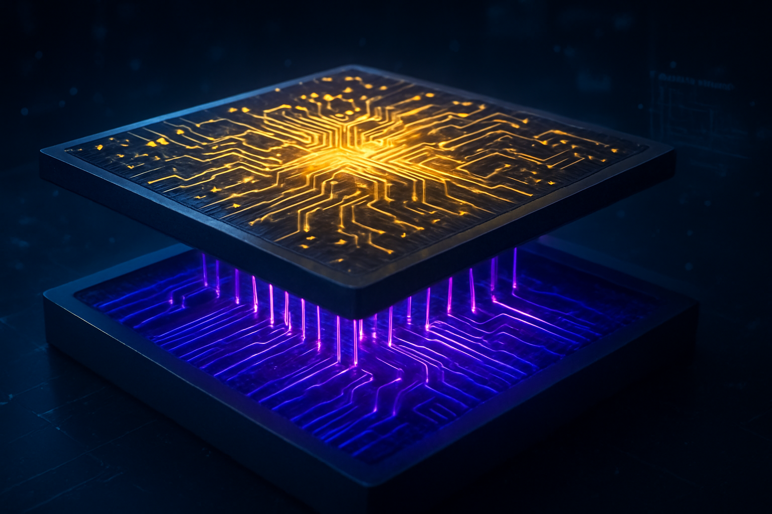
The Physics of the 'Copper Wall' and the Rise of 1.6T Optics
The technical crisis that precipitated this shift is known as the "Copper Wall." As per-lane speeds reached 224 Gbps in late 2024 and throughout 2025, the reach of passive copper cables plummeted to less than one meter. At these frequencies, electrical signals degrade so rapidly that they can barely traverse a single server rack without massive power-hungry amplification. By early 2025, data center operators reported that the "I/O Tax"—the energy required just to move data between chips—was consuming nearly 30% of total cluster power.
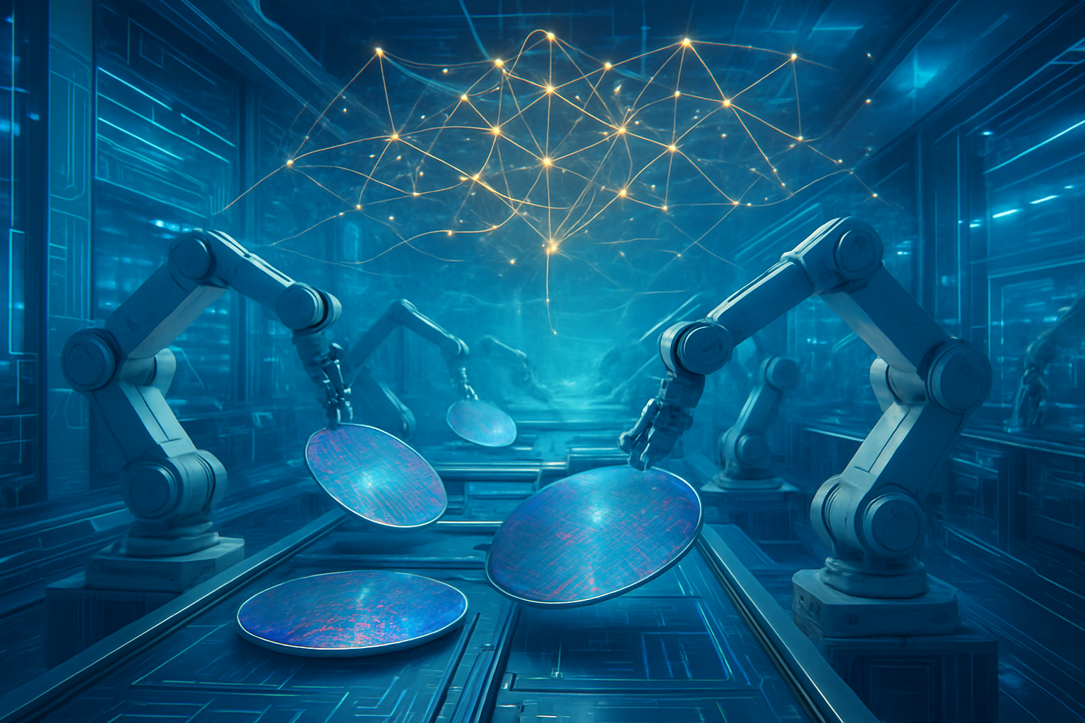
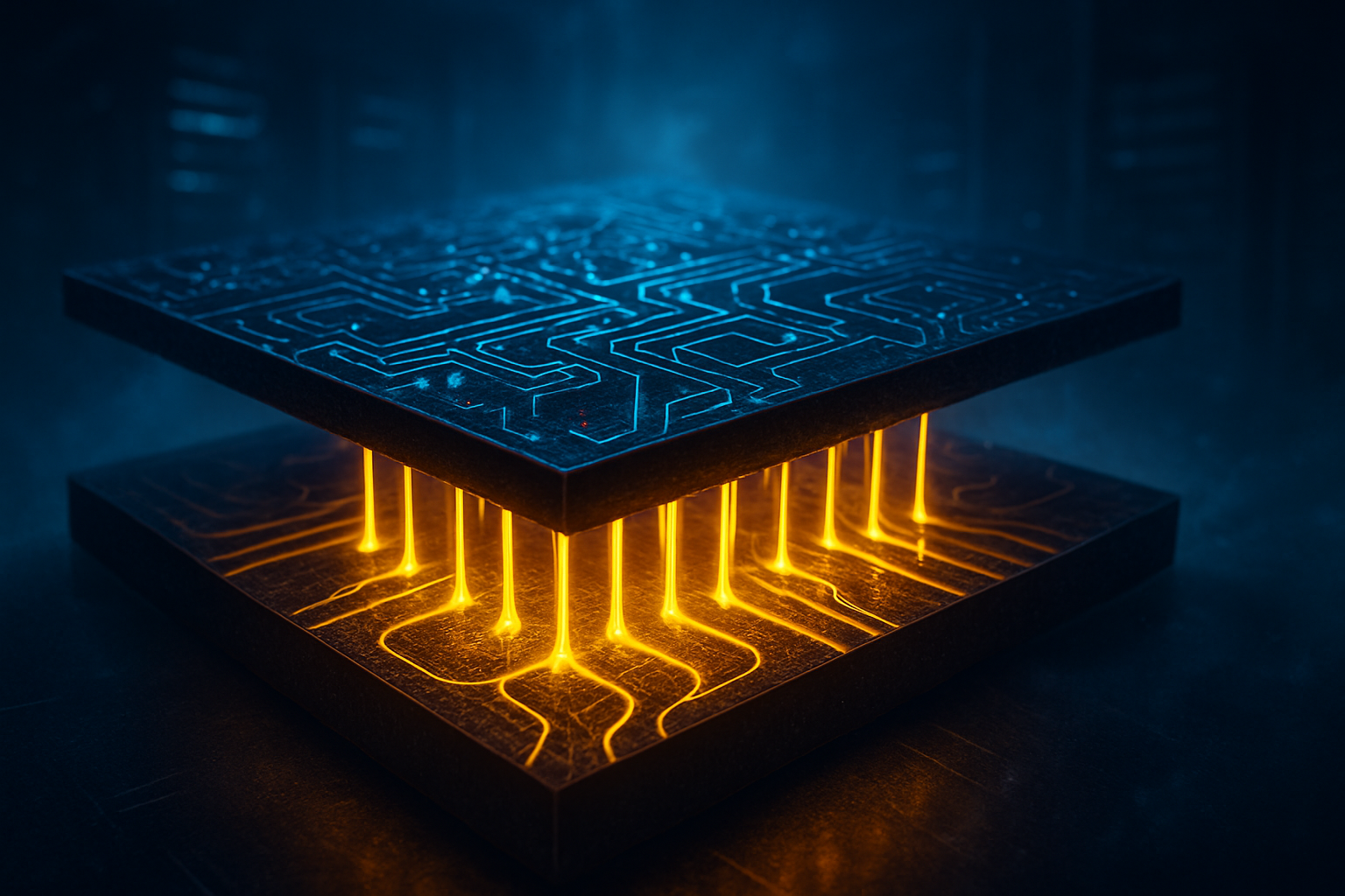
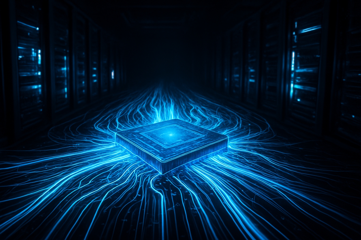
To solve this, the industry has turned to Co-Packaged Optics (CPO) and Silicon Photonics. Unlike traditional pluggable transceivers that sit at the edge of a switch, CPO moves the optical engine directly onto the processor substrate. This allows for a "shoreline" of high-speed optical I/O that bypasses the energy losses of long electrical traces. In late 2025, the market saw the mass adoption of 1.6T (Terabit) transceivers, which utilize 200G per-lane technology. By early 2026, initial demonstrations of 3.2T links using 400G per-lane technology have already begun, promising to support the massive throughput required for real-time inference on trillion-parameter models.
The technical community has also embraced Linear-drive Pluggable Optics (LPO) as a bridge technology. By removing the power-intensive Digital Signal Processor (DSP) from the optical module and relying on the host ASIC to drive the signal, LPO has provided a lower-latency, lower-power intermediate step. However, for the most advanced AI clusters, CPO is now considered the "gold standard," as it reduces energy consumption from approximately 15 picojoules per bit (pJ/bit) to less than 5 pJ/bit.
The New Power Players: NVDA, AVGO, and the Optical Arms Race
The transition to light has fundamentally shifted the competitive dynamics among semiconductor giants. Nvidia (NASDAQ: NVDA) has solidified its dominance by integrating silicon photonics into its latest Rubin architecture and Quantum-X networking platforms. By utilizing optical NVLink fabrics, Nvidia’s million-GPU clusters can now operate with nanosecond latency, effectively treating an entire data center as a single, massive GPU.
Broadcom (NASDAQ: AVGO) has emerged as a primary architect of this new era with its Tomahawk 6-Davisson switch, which boasts a staggering 102.4 Tbps throughput and integrated CPO. Broadcom’s success in proving CPO reliability at scale—particularly within the massive AI infrastructures of Meta and Google—has made it the indispensable partner for optical networking. Meanwhile, TSMC (NYSE: TSM) has become the foundational foundry for this transition through its COUPE (Compact Universal Photonic Engine) technology, which allows for the 3D stacking of photonic and electronic circuits, a feat previously thought to be years away from mass production.
Other key players are carving out critical niches in the optical ecosystem. Marvell (NASDAQ: MRVL), following its strategic acquisition of optical interconnect startups in late 2025, has positioned its Ara 1.6T Optical DSP as the backbone for third-party AI accelerators. Intel (NASDAQ: INTC) has also made a significant comeback in the data center space with its Optical Compute Interconnect (OCI) chiplets. Intel’s unique ability to integrate lasers directly onto the silicon die has enabled "disaggregated" data centers, where compute and memory can be physically separated by over 100 meters without a loss in performance, a capability that is revolutionizing how hyperscalers design their facilities.
Sustainability and the Global Interconnect Pivot
The wider significance of the move from copper to light extends far beyond mere speed. In an era where the energy demands of AI have become a matter of national security and environmental concern, silicon photonics offers a rare "win-win" for both performance and sustainability. The 70% reduction in interconnect power provided by CPO is critical for meeting the carbon-neutral goals of tech giants like Microsoft and Amazon, who are currently retrofitting their global data center fleets to support optical fabrics.
Furthermore, this transition marks the end of the "Compute-Bound" era and the beginning of the "Interconnect-Bound" era. For years, the bottleneck in AI was the speed of the processor itself. Today, the bottleneck is the "fabric"—the ability to move massive amounts of data between thousands of processors simultaneously. By shattering the Copper Wall, the industry has ensured that AI scaling laws can continue to hold true for the foreseeable future.
However, this shift is not without its concerns. The complexity of manufacturing CPO-based systems is significantly higher than traditional copper-based ones, leading to potential supply chain vulnerabilities. There are also ongoing debates regarding the "serviceability" of integrated optics; if an optical laser fails inside a $40,000 GPU package, the entire unit may need to be replaced, unlike the "hot-swappable" pluggable modules of the past.
The Road to Petabit Connectivity and Optical Computing
Looking ahead to the remainder of 2026 and into 2027, the industry is already eyeing the next frontier: Petabit-per-second connectivity. As 3.2T transceivers move into production, researchers are exploring multi-wavelength "comb lasers" that can transmit hundreds of data streams over a single fiber, potentially increasing bandwidth density by another order of magnitude.
Beyond just moving data, the ultimate goal is Optical Computing—performing mathematical calculations using light itself rather than transistors. While still in the early experimental stages, the integration of photonics into the processor package is the necessary first step toward this "Holy Grail" of computing. Experts predict that by 2028, we may see the first hybrid "Opto-Electronic" processors that perform specific AI matrix multiplications at the speed of light, with virtually zero heat generation.
The immediate challenge remains the standardization of CPO interfaces. Groups like the OIF (Optical Internetworking Forum) are working feverishly to ensure that components from different vendors can interoperate, preventing the "walled gardens" that could stifle innovation in the optical ecosystem.
Conclusion: A Bright Future for AI Infrastructure
The transition from copper to silicon photonics represents one of the most significant architectural shifts in the history of computing. By overcoming the physical limitations of electricity, the industry has laid the groundwork for AGI-scale infrastructure that is faster, more efficient, and more scalable than anything that came before. The "Copper Era," which defined the first fifty years of the digital age, has finally given way to the "Era of Light."
As we move further into 2026, the key metrics to watch will be the yield rates of CPO-integrated chips and the speed at which 1.6T networking is deployed across global data centers. For AI companies and tech enthusiasts alike, the message is clear: the future of intelligence is no longer traveling through wires—it is moving at the speed of light.
This content is intended for informational purposes only and represents analysis of current AI developments.
TokenRing AI delivers enterprise-grade solutions for multi-agent AI workflow orchestration, AI-powered development tools, and seamless remote collaboration platforms.
For more information, visit https://www.tokenring.ai/.