On December 17, 2025, the landscape of American semiconductor manufacturing shifted as Texas Instruments (NASDAQ: TXN) officially commenced production at its SM1 fab in Sherman, Texas. This milestone marks the first of four planned facilities at the site, representing a massive $30 billion investment aimed at securing the foundational silicon supply chain. As of January 1, 2026, the facility is actively ramping up its output, signaling a pivotal moment in the "Global Reshoring Boom" that seeks to return high-tech manufacturing to U.S. soil.
The opening of SM1 is not merely a corporate expansion; it is a strategic maneuver to provide the essential components that power the modern world. While much of the public's attention remains fixed on high-end logic processors, the Sherman facility focuses on the "foundational" chips—analog and embedded processors—that are the unsung heroes of the AI revolution and the automotive industry’s transition to electrification. By internalizing its supply chain, Texas Instruments is positioning itself as a cornerstone of industrial stability in an increasingly volatile global market.
Technical Specifications and the 300mm Advantage
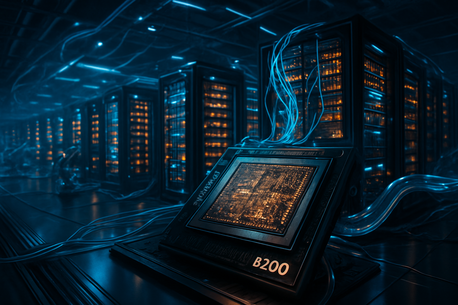
The SM1 facility is a marvel of modern engineering, specifically designed to produce 300mm (12-inch) wafers. This transition from the industry-standard 200mm wafers is a game-changer for Texas Instruments, providing 2.3 times more surface area per wafer. This shift is expected to yield an estimated 40% reduction in chip-level fabrication costs, allowing the company to maintain high margins while providing competitive pricing for the massive volumes required by the AI and automotive sectors.
Unlike the sub-5nm "bleeding edge" nodes used for CPUs and GPUs, the Sherman site operates primarily in the 28nm to 130nm range. These "mature" nodes are the sweet spot for high-performance analog and embedded processing. These chips are designed for durability, high-voltage precision, and thermal stability—qualities essential for power management in AI data centers and battery management systems in electric vehicles (EVs). Initial reactions from industry experts suggest that TI's focus on these foundational nodes is a masterstroke, addressing the specific types of chip shortages that paralyzed the global economy in the early 2020s.
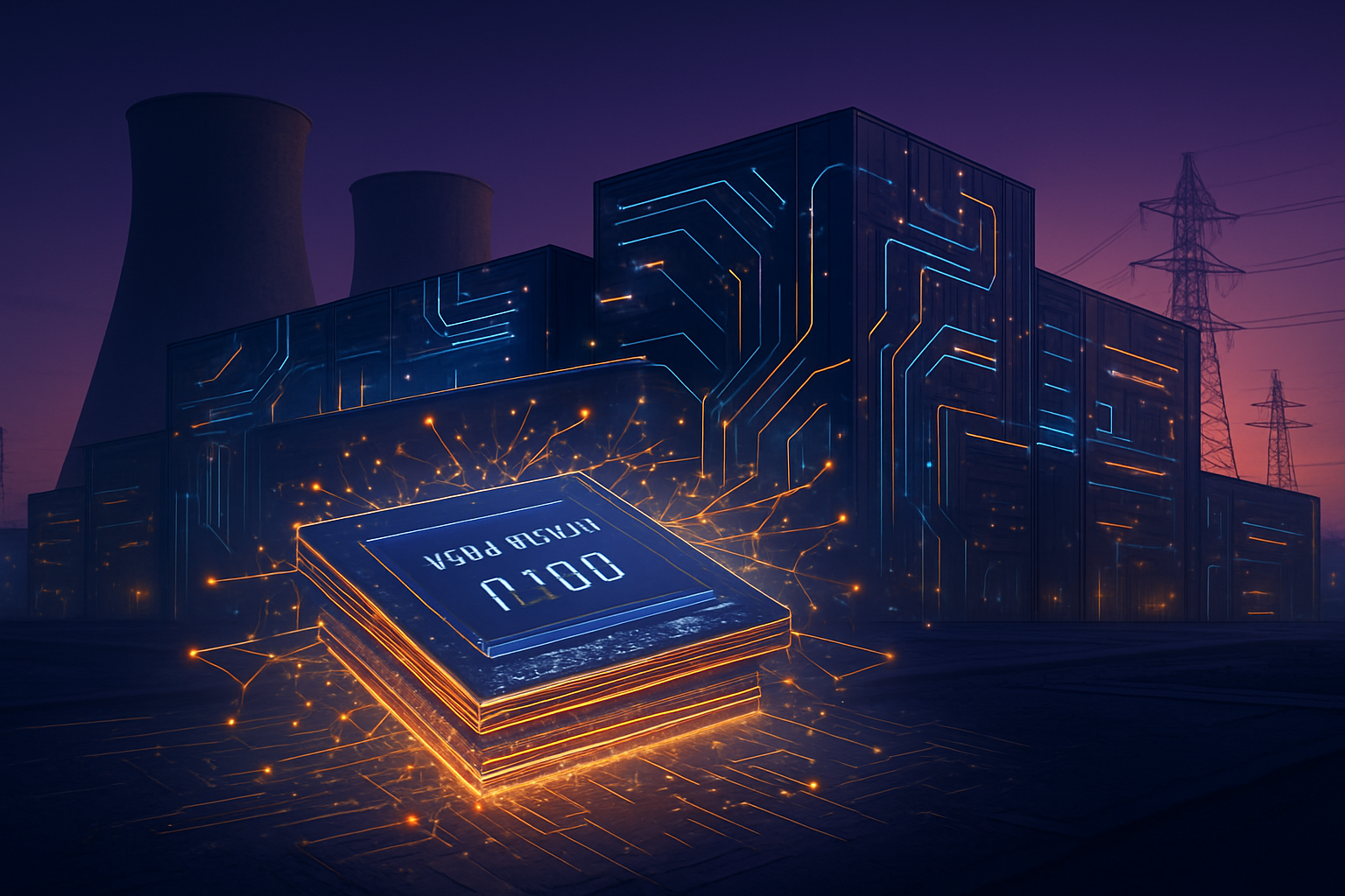
The facility’s output includes advanced multiphase controllers and smart power stages. These components are critical for the 800VDC architectures now becoming standard in AI data centers, where they manage the intense power delivery required by high-performance AI accelerators. Furthermore, the fab is producing the latest Sitara™ AM69A processors, which are optimized for "Edge AI" applications, enabling autonomous robots and smart vehicles to perform complex computer vision tasks with minimal power consumption.
Market Impact: Powering the AI Giants and Automakers
The start of production at SM1 has immediate implications for tech giants and AI startups alike. As companies like NVIDIA (NASDAQ: NVDA) and Advanced Micro Devices (NASDAQ: AMD) push the limits of compute power, they require an equally sophisticated "nervous system" of power management and signal chain components to keep their chips running. Texas Instruments is now positioned to be the primary domestic supplier of these components, offering a "geopolitically dependable" supply chain that mitigates the risks associated with overseas foundries.
For the automotive sector, the Sherman fab is a lifeline. Major U.S. automakers, including Ford (NYSE: F) and Tesla (NASDAQ: TSLA), stand to benefit from a localized supply of chips used in battery management, advanced driver-assistance systems (ADAS), and vehicle-to-everything (V2X) communication. By manufacturing these chips in Texas, TI reduces lead times and provides a buffer against the supply shocks that have historically disrupted vehicle production lines.
This move also places significant pressure on international competitors like Infineon and Analog Devices (NASDAQ: ADI). By aiming to manufacture more than 95% of its chips internally by 2030, Texas Instruments is aggressively decoupling from external foundries. This vertical integration provides a strategic advantage in terms of cost control and quality assurance, potentially allowing TI to capture a larger share of the industrial and automotive markets as they continue to digitize and electrify.
The Global Reshoring Boom and Geopolitical Stability
The Sherman mega-site is a flagship project of the broader U.S. effort to reclaim semiconductor sovereignty. Supported by $1.6 billion in direct funding from the CHIPS and Science Act, as well as billions more in investment tax credits, the project is a testament to the success of federal incentives in driving domestic manufacturing. This "Global Reshoring Boom" is a response to the vulnerabilities exposed by the global pandemic and rising geopolitical tensions, which highlighted the danger of over-reliance on a few concentrated manufacturing hubs in East Asia.
In the broader AI landscape, the SM1 fab represents the "infrastructure layer" that makes large-scale AI deployment possible. While software breakthroughs often grab the headlines, those breakthroughs cannot be realized without the physical hardware to support them. TI’s investment ensures that as AI moves from experimental labs into every facet of the industrial and consumer world, the foundational hardware will be available and sustainably sourced.
However, the rapid expansion of such massive facilities also brings concerns regarding resource consumption and labor. The Sherman site is expected to support 3,000 direct jobs, but the demand for highly skilled technicians and engineers remains a challenge for the North Texas region. Furthermore, the environmental impact of large-scale semiconductor fabrication—specifically water and energy usage—remains a point of scrutiny, though TI has committed to utilizing advanced recycling and sustainable building practices for the Sherman campus.
The Road to 100 Million Chips Per Day
Looking ahead, the opening of SM1 is only the beginning. The exterior shell for the second fab, SM2, is already complete, with cleanroom installation and tool positioning scheduled to begin later in 2026. Two additional fabs, SM3 and SM4, are planned for future phases, with the ultimate goal of producing over 100 million chips per day at the Sherman site alone. This roadmap suggests that Texas Instruments is betting heavily on a long-term, sustained demand for foundational silicon.
In the near term, we can expect to see TI release a new generation of "intelligent" analog chips that integrate more AI-driven monitoring and self-diagnostic features directly into the hardware. These will be crucial for the next generation of smart grids, medical devices, and industrial automation. Experts predict that the Sherman site will become the epicenter of a new "Silicon Prairie," attracting a cluster of satellite industries and suppliers to North Texas.
The challenge for TI will be maintaining this momentum as global economic conditions fluctuate. While the current demand for AI and EV silicon is high, the semiconductor industry is notoriously cyclical. However, by focusing on the foundational chips that are required regardless of which specific AI model or vehicle brand wins the market, TI has built a resilient business model that is well-positioned for the decades to come.
A New Era for American Silicon
The commencement of production at Texas Instruments' SM1 fab is a landmark achievement in the history of American technology. It signifies a shift away from the "fab-lite" models of the past two decades and a return to the era of the integrated device manufacturer. By combining cutting-edge 300mm fabrication with a strategic focus on the essential components of the modern economy, TI is not just building chips; it is building a foundation for the next century of innovation.
As we move further into 2026, the success of the Sherman site will be a bellwether for the success of the CHIPS Act and the broader reshoring movement. The ability to produce 100 million chips a day domestically would be a transformative shift in the global supply chain, providing the stability and scale needed to fuel the AI-driven future. For now, the lights are on in Sherman, and the first wafers are rolling off the line—a clear signal that the American semiconductor industry is back in the driver's seat.
This content is intended for informational purposes only and represents analysis of current AI developments.
TokenRing AI delivers enterprise-grade solutions for multi-agent AI workflow orchestration, AI-powered development tools, and seamless remote collaboration platforms.
For more information, visit https://www.tokenring.ai/.