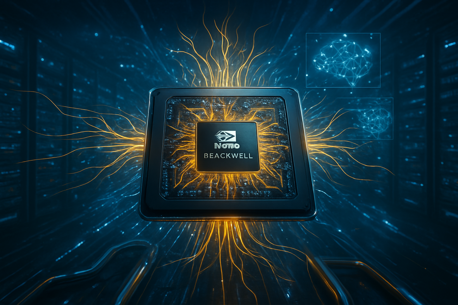
In a move that signals the definitive end of the "copper era" for high-performance computing, Marvell Technology (NASDAQ: MRVL) has announced the acquisition of photonic interconnect pioneer Celestial AI for $3.25 billion. The deal, finalized in late 2025, centers on Celestial AI’s revolutionary "Photonic Fabric" technology, a breakthrough that allows AI accelerators to communicate via light directly from the silicon die. As global demand for AI training capacity pushes data centers toward million-GPU clusters, the acquisition positions Marvell as the primary architect of the optical nervous system required to sustain the next generation of generative AI.
The significance of this acquisition cannot be overstated. By integrating Celestial AI’s optical chiplets and interposers into its existing portfolio of high-speed networking silicon, Marvell is addressing the "Memory Wall" and the "Power Wall"—the two greatest physical barriers currently facing the semiconductor industry. As traditional copper-based electrical links reach their physical limits at 224G per lane, the transition to optical fabrics is no longer an elective upgrade; it is a fundamental requirement for the survival of the AI scaling laws.
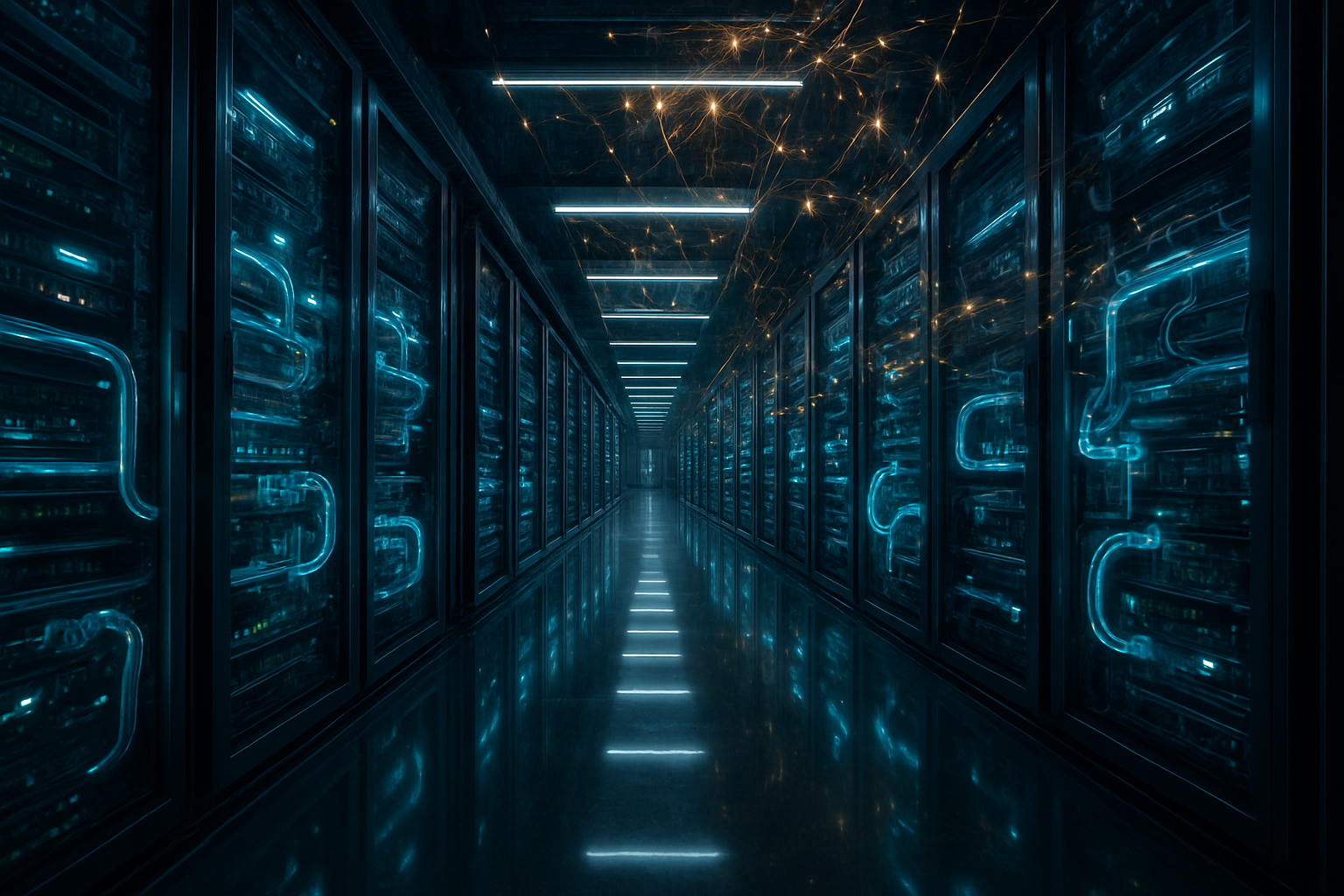
The End of the Copper Cliff: Technical Breakdown of the Photonic Fabric
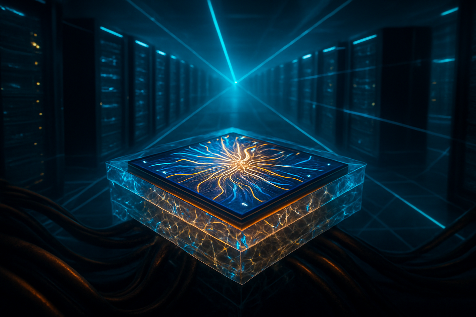
At the heart of the acquisition is Celestial AI’s Photonic Fabric, a technology that replaces traditional electrical "beachfront" I/O with high-density optical signals. While current data centers rely on Active Electrical Cables (AECs) or pluggable optical transceivers, these methods introduce significant latency and power overhead. Celestial AI’s PFLink™ chiplets provide a staggering 14.4 to 16 Terabits per second (Tbps) of optical bandwidth per chiplet—roughly 25 times the bandwidth density of current copper-based solutions. This allows for "scale-up" interconnects that treat an entire rack of GPUs as a single, massive compute node.
Furthermore, the Photonic Fabric utilizes an Optical Multi-Die Interposer (OMIB™), which enables the disaggregation of compute and memory. In traditional architectures, High Bandwidth Memory (HBM) must be placed in immediate proximity to the GPU to maintain speed, limiting total memory capacity. With Celestial AI’s technology, Marvell can now offer architectures where a single XPU can access a pool of up to 32TB of shared HBM3E or DDR5 memory at nanosecond-class latencies (approximately 250–300 ns). This "optical memory pooling" effectively shatters the memory bottlenecks that have plagued LLM training.
The efficiency gains are equally transformative. Operating at approximately 2.4 picojoules per bit (pJ/bit), the Photonic Fabric offers a 10x reduction in power consumption compared to the energy-intensive SerDes (Serializer/Deserializer) processes required to drive signals through copper. This reduction is critical as data centers face increasingly stringent thermal and power constraints. Initial reactions from the research community suggest that this shift could reduce the total cost of ownership for AI clusters by as much as 30%, primarily through energy savings and simplified thermal management.
Shifting the Balance of Power: Market and Competitive Implications
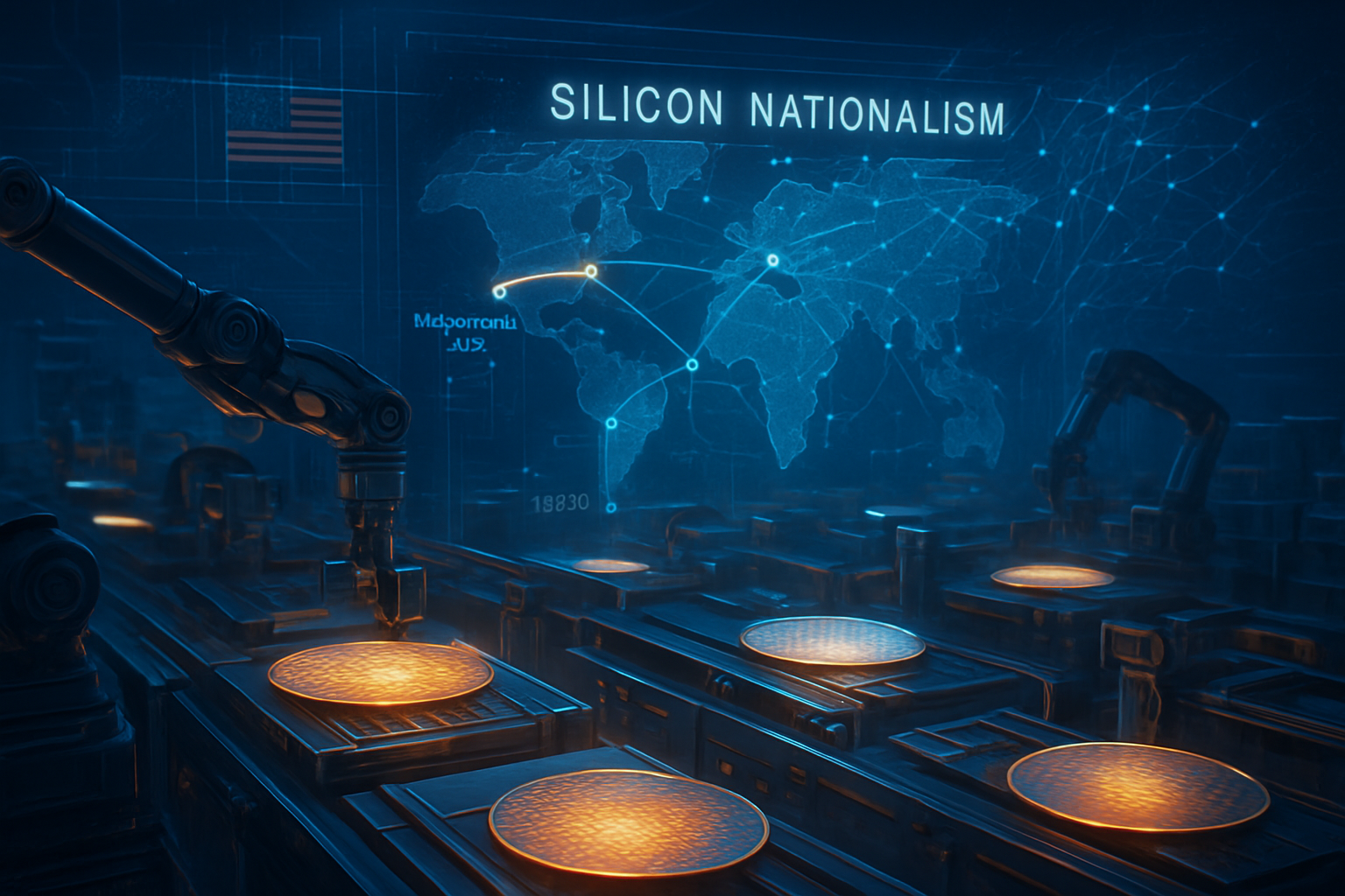
The acquisition places Marvell in a formidable position against its primary rival, Broadcom (NASDAQ: AVGO), which has dominated the high-end switch and custom ASIC market for years. While Broadcom has focused on Co-Packaged Optics (CPO) and its Tomahawk switch series, Marvell’s integration of the Photonic Fabric provides a more holistic "die-to-die" and "rack-to-rack" optical solution. This deal allows Marvell to offer hyperscalers like Amazon (NASDAQ: AMZN) and Meta (NASDAQ: META) a complete, vertically integrated stack—from the 1.6T Ara optical DSPs to the Teralynx 10 switch silicon and now the Photonic Fabric interconnects.
For AI giants like NVIDIA (NASDAQ: NVDA), the move is both a challenge and an opportunity. While NVIDIA’s NVLink has been the gold standard for GPU-to-GPU communication, it remains largely proprietary and electrical at the board level. Marvell’s new technology offers an open-standard alternative (via CXL and UCIe) that could allow other chipmakers, such as AMD (NASDAQ: AMD) or Intel (NASDAQ: INTC), to build competitive multi-chip clusters that rival NVIDIA’s performance. This democratization of high-speed interconnects could potentially erode NVIDIA’s "moat" by allowing a broader ecosystem of hardware to perform at the same scale.
Industry analysts suggest that the $3.25 billion price tag is a steal given the strategic importance of the intellectual property involved. Celestial AI had previously secured backing from heavyweights like Samsung (KRX: 005930) and AMD Ventures, indicating that the industry was already coalescing around its "optical-first" vision. By bringing this technology in-house, Marvell ensures that it is no longer just a component supplier but a platform provider for the entire AI infrastructure layer.
The Broader Significance: Navigating the Energy Crisis of AI
Beyond the immediate corporate rivalry, the Marvell-Celestial AI deal addresses a looming crisis in the AI landscape: sustainability. The current trajectory of AI training consumes vast amounts of electricity, with a significant portion of that energy wasted as heat generated by electrical resistance in copper wiring. As we move toward 1.6T and 3.2T networking speeds, the "Copper Cliff" becomes a physical wall; signal attenuation at these frequencies is so high that copper traces can only travel a few inches before the data becomes unreadable.
By transitioning to an all-optical fabric, the industry can extend the reach of high-speed signals from centimeters to meters—and even kilometers—without significant signal degradation or heat buildup. This allows for the creation of "geographically distributed clusters," where different parts of a single AI training job can be spread across multiple buildings or even cities, linked by Marvell’s COLORZ 800G coherent optics and the new Photonic Fabric.
This milestone is being compared to the transition from vacuum tubes to transistors or the shift from spinning hard drives to SSDs. It represents a fundamental change in the medium of computation. Just as the internet was revolutionized by the move from copper phone lines to fiber optics, the internal architecture of the computer is now undergoing the same transformation. The "Optical Era" of computing has officially arrived, and it is powered by silicon photonics.
Looking Ahead: The Roadmap to 2030
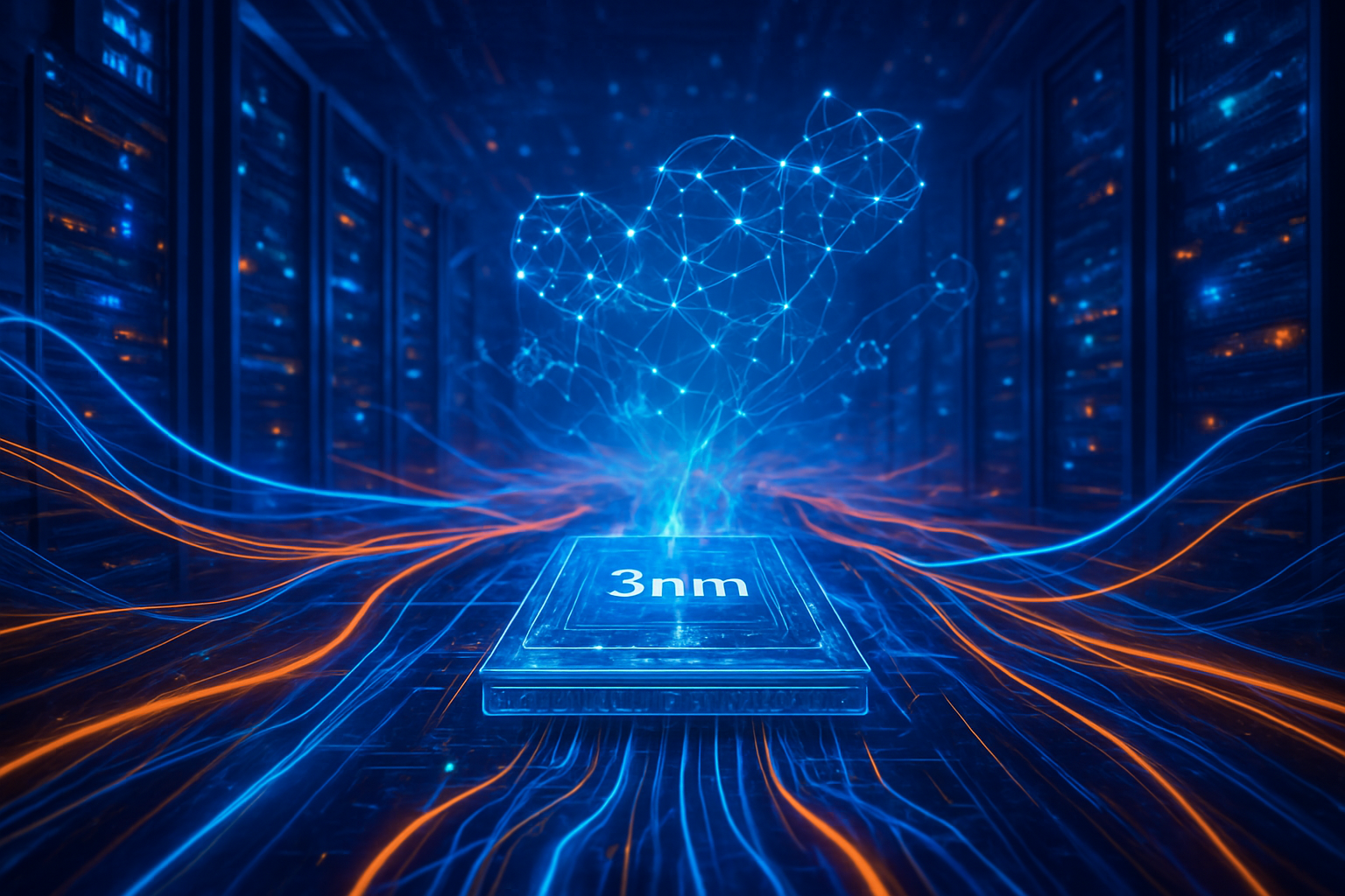
In the near term, expect Marvell to integrate Photonic Fabric chiplets into its 3nm and 2nm custom ASIC roadmaps. We are likely to see the first "Super XPUs"—processors with integrated optical I/O—hitting the market by early 2027. These chips will enable the first true million-GPU clusters, capable of training models with tens of trillions of parameters in a fraction of the time currently required.
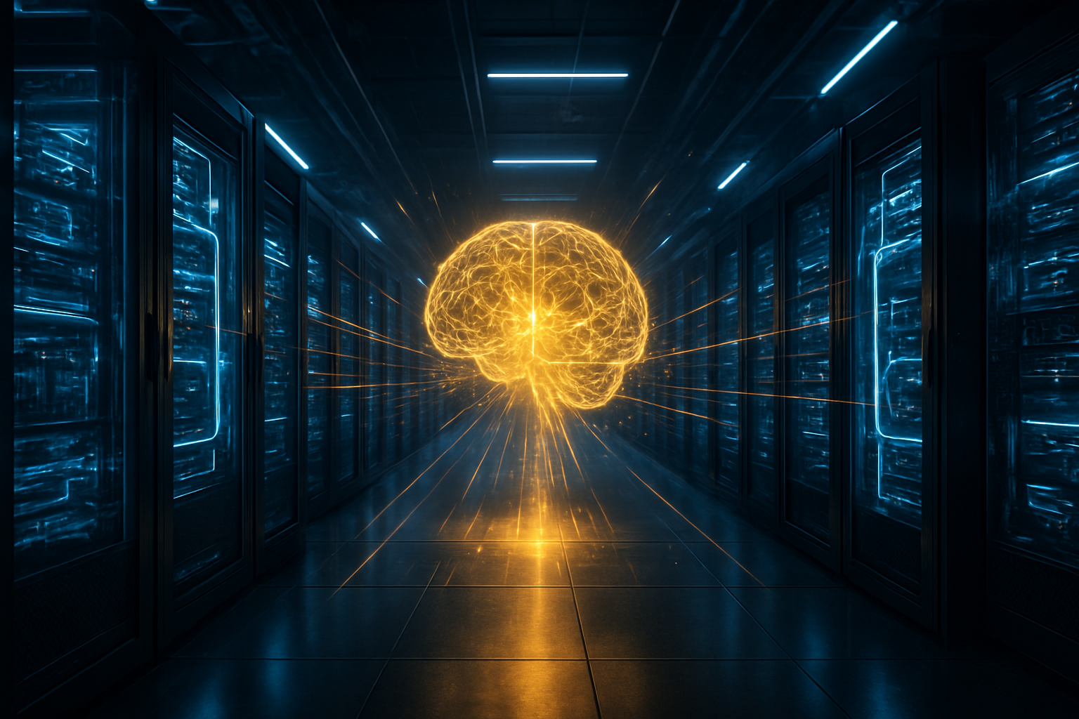
The next frontier will be the integration of optical computing itself. While the Photonic Fabric currently focuses on moving data via light, companies are already researching how to perform mathematical operations using light (optical matrix multiplication). Marvell’s acquisition of Celestial AI provides the foundational packaging and interconnect technology that will eventually support these future optical compute engines. The primary challenge remains the manufacturing yield of complex silicon photonics at scale, but with Marvell’s manufacturing expertise and TSMC’s (NYSE: TSM) advanced packaging capabilities, these hurdles are expected to be cleared within the next 24 months.
A New Foundation for Artificial Intelligence
The acquisition of Celestial AI by Marvell Technology marks a historic pivot in the evolution of AI infrastructure. It is a $3.25 billion bet that the future of intelligence is light-based. By solving the dual bottlenecks of bandwidth and power, Marvell is not just building faster chips; it is enabling the physical architecture that will support the next decade of AI breakthroughs.
As we look toward 2026, the industry will be watching closely to see how quickly Marvell can productize the Photonic Fabric and whether competitors like Broadcom will respond with their own major acquisitions. For now, the message is clear: the era of the copper-bound data center is over, and the race to build the first truly optical AI supercomputer has begun.
This content is intended for informational purposes only and represents analysis of current AI developments.
TokenRing AI delivers enterprise-grade solutions for multi-agent AI workflow orchestration, AI-powered development tools, and seamless remote collaboration platforms.
For more information, visit https://www.tokenring.ai/.