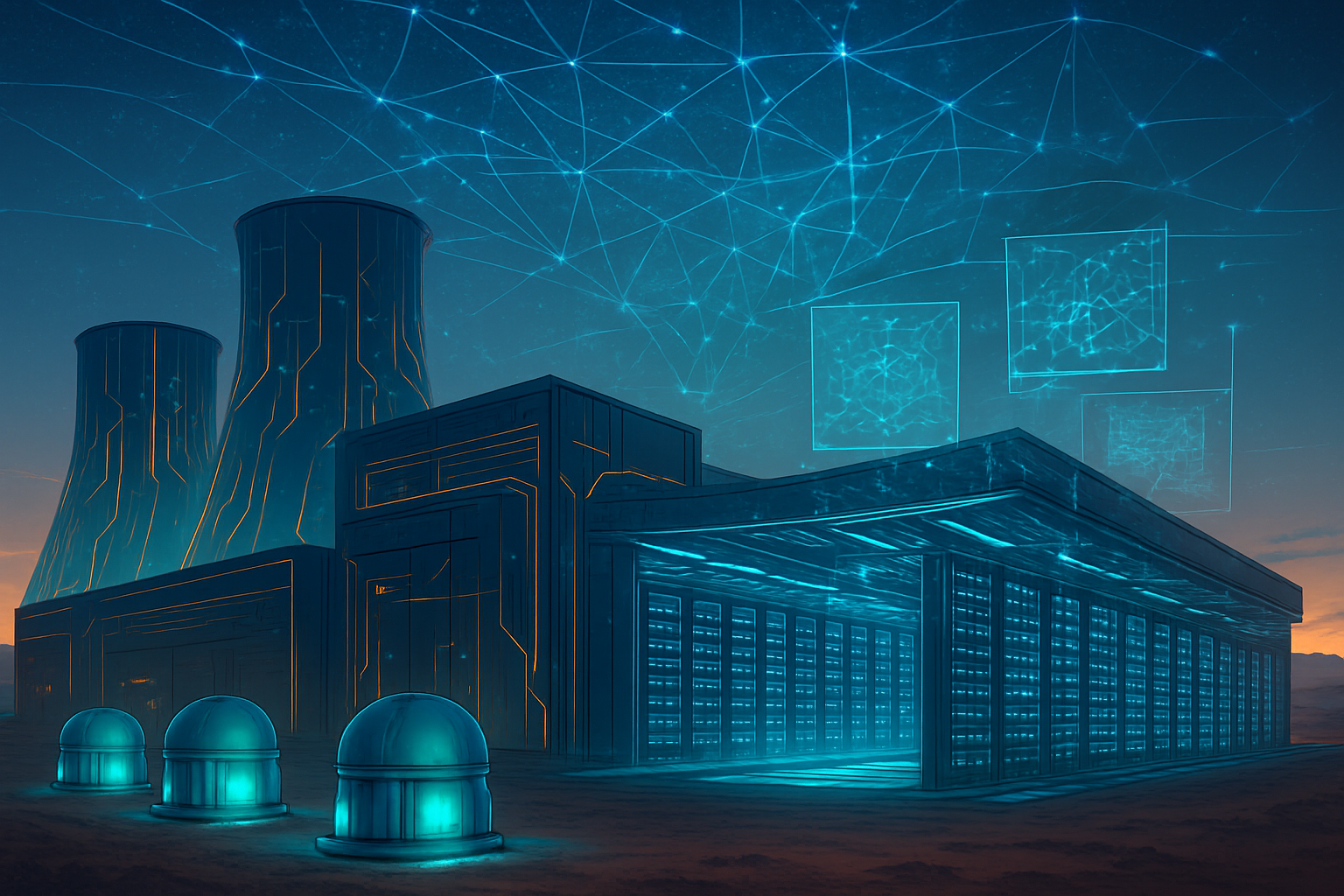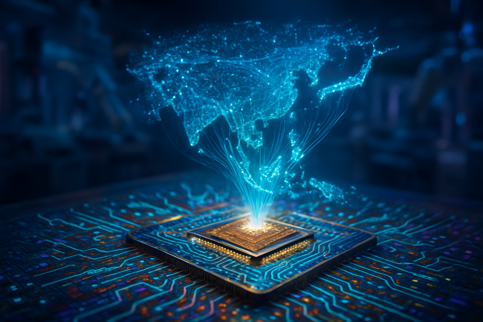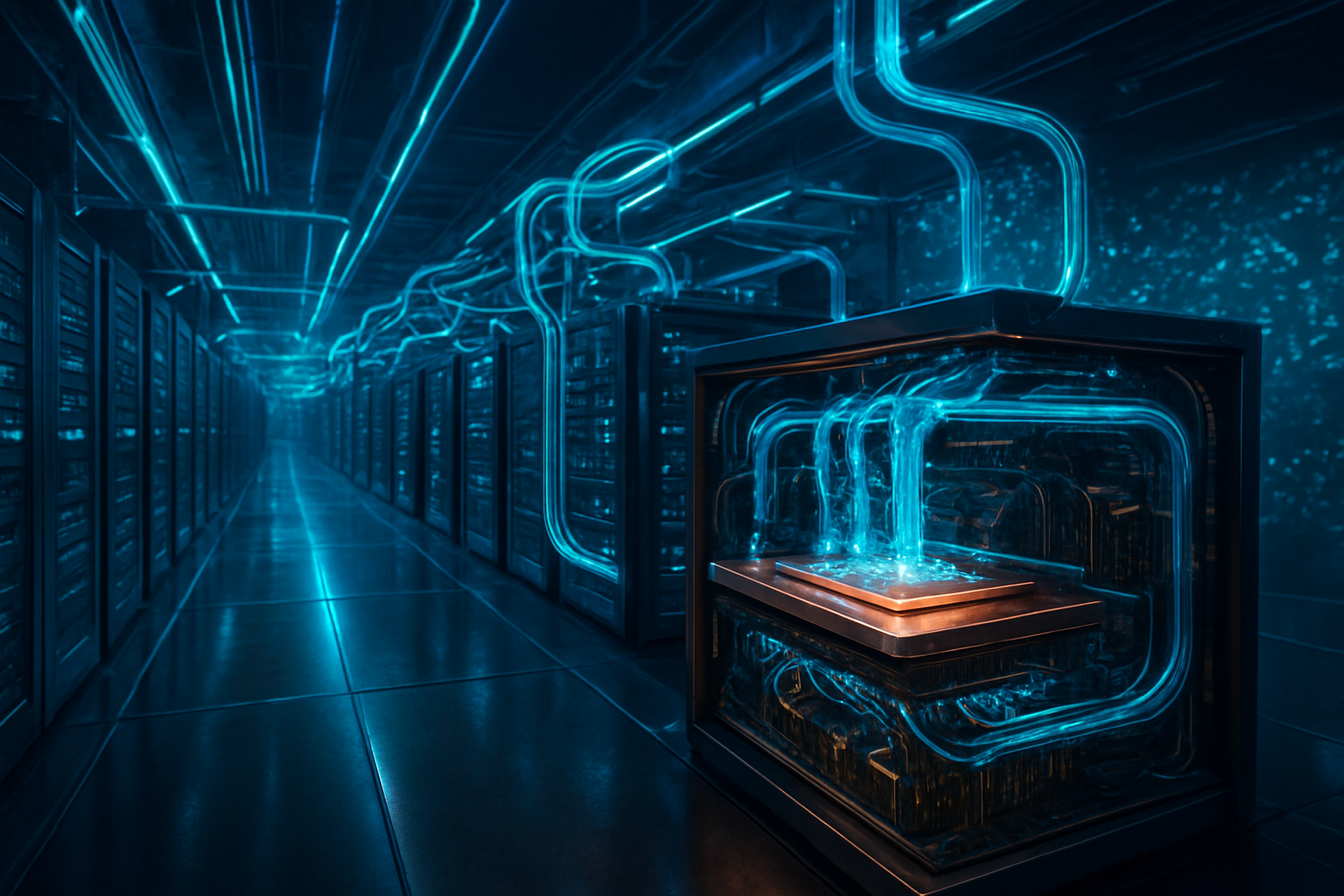
In a move that cements its dominance over the artificial intelligence landscape, Nvidia (NASDAQ:NVDA) has officially moved its Blackwell GPU architecture into full-scale volume production. This milestone marks the beginning of a new chapter in computational history, as the company scales its most powerful hardware to meet the insatiable demand of hyperscalers and sovereign nations alike. With CEO Jensen Huang confirming that the company is now shipping approximately 1,000 Blackwell GB200 NVL72 racks per week, the "AI Factory" has transitioned from a conceptual vision to a physical reality, promising to redefine the economics of large-scale model deployment.
The production ramp-up is accompanied by two significant breakthroughs that are already rippling through the industry: a staggering 25x increase in efficiency for trillion-parameter models and the launch of the RTX PRO 5000 72GB variant. These developments address the two most critical bottlenecks in the current AI era—energy consumption at the data center level and memory constraints at the developer workstation level. As the industry shifts its focus from training massive models to the high-volume inference required for agentic AI, Nvidia's latest hardware rollout appears perfectly timed to capture the next wave of the AI revolution.
Technical Mastery: FP4 Precision and the 72GB Workstation Powerhouse
The technical cornerstone of the Blackwell architecture's success is its revolutionary 4-bit floating point (FP4) precision. By introducing this new numerical format, Nvidia has effectively doubled the throughput of its previous H100 "Hopper" architecture while maintaining the high levels of accuracy required for trillion-parameter Mixture-of-Experts (MoE) models. This advancement, powered by 5th Generation Tensor Cores, allows the GB200 NVL72 systems to deliver up to 30x the inference performance of equivalent H100 clusters. The result is a hardware ecosystem that can process the world’s most complex AI tasks with significantly lower latency and a fraction of the power footprint previously required.
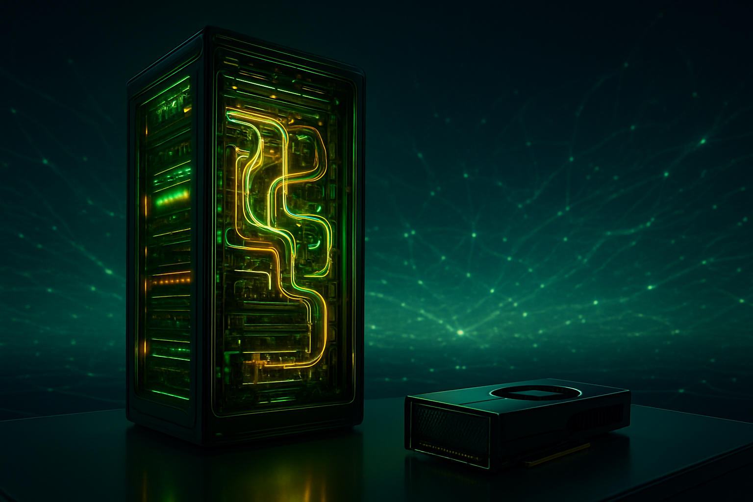
Beyond the data center, Nvidia has addressed the needs of local developers with the October 21, 2025, launch of the RTX PRO 5000 72GB. This workstation-class GPU, built on the Blackwell GB202 architecture, features a massive 72GB of GDDR7 memory with Error Correction Code (ECC) support. With 14,080 CUDA cores and a staggering 2,142 TOPS of AI performance, the card is designed specifically for "Agentic AI" development and the local fine-tuning of large models. By offering a 50% increase in VRAM over its predecessor, the RTX PRO 5000 72GB allows engineers to keep massive datasets in local memory, ensuring data privacy and reducing the high costs associated with constant cloud prototyping.
Initial reactions from the AI research community have been overwhelmingly positive, particularly regarding the efficiency gains. Early benchmarks from major labs suggest that the 25x reduction in energy consumption for trillion-parameter inference is not just a theoretical marketing claim but a practical reality in production environments. Industry experts note that the Blackwell architecture’s ability to run these massive models on fewer nodes significantly reduces the "communication tax"—the energy and time lost when data travels between different chips—making the GB200 the most cost-effective platform for the next generation of generative AI.
Market Domination and the Competitive Fallout
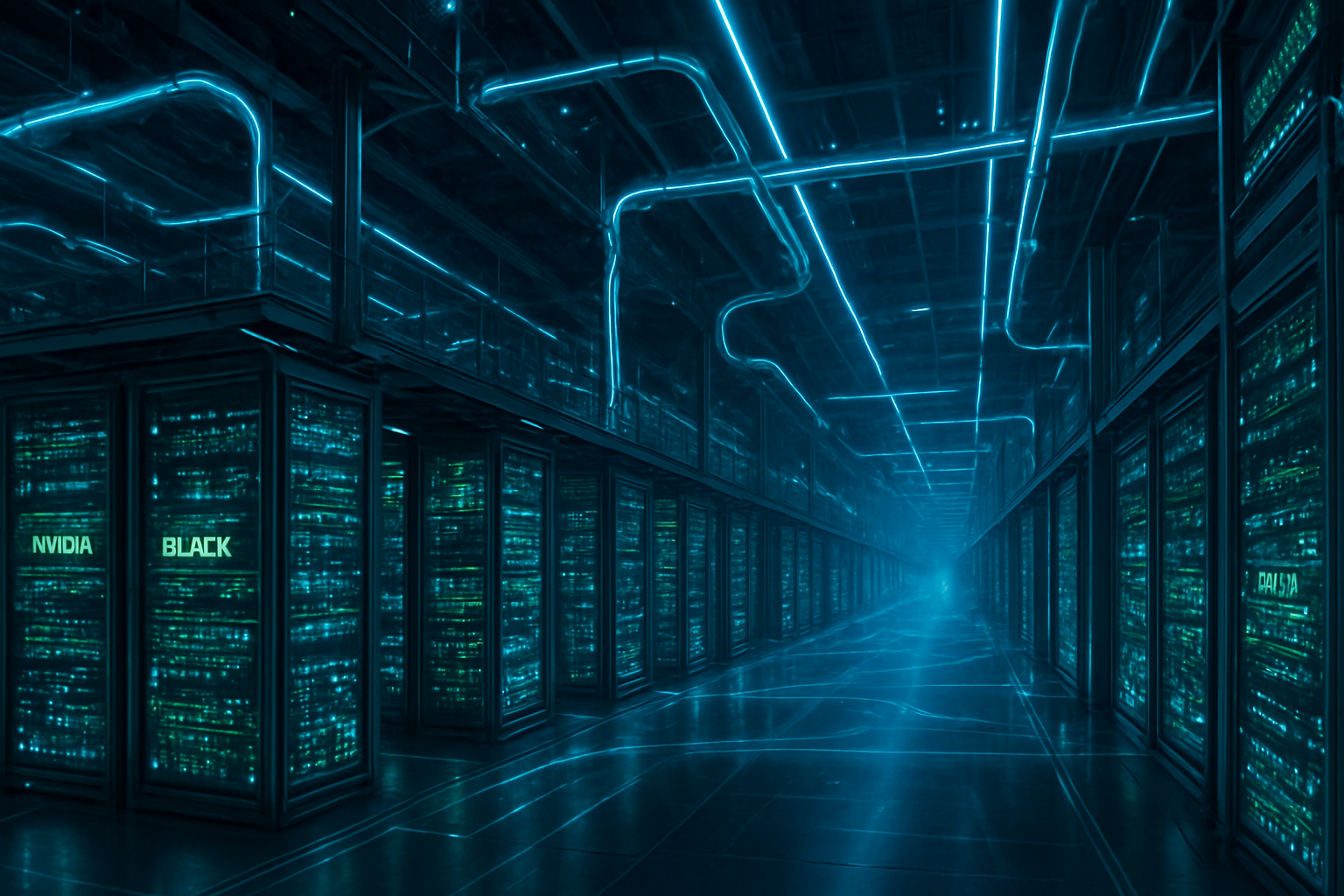
The full-scale production of Blackwell has profound implications for the world's largest tech companies. Hyperscalers such as Microsoft (NASDAQ:MSFT), Alphabet (NASDAQ:GOOGL), and Amazon (NASDAQ:AMZN) have already integrated Blackwell into their cloud offerings. Microsoft Azure’s ND GB200 V6 series and Google Cloud’s A4 VMs are now generally available, providing the infrastructure necessary for enterprises to deploy agentic workflows at scale. This rapid adoption has translated into a massive financial windfall for Nvidia, with Blackwell-related revenue reaching an estimated $11 billion in the final quarter of 2025 alone.
For competitors like Advanced Micro Devices (NASDAQ:AMD) and Intel (NASDAQ:INTC), the Blackwell production ramp presents a daunting challenge. While AMD’s MI300 and MI325X series have found success in specific niches, Nvidia’s ability to ship 1,000 full-rack systems per week creates a "moat of scale" that is difficult to breach. The integration of hardware, software (CUDA), and networking (InfiniBand/Spectrum-X) into a single "AI Factory" platform makes it increasingly difficult for rivals to offer a comparable total cost of ownership (TCO), especially as the market shifts its spending from training to high-efficiency inference.
Furthermore, the launch of the RTX PRO 5000 72GB disrupts the professional workstation market. By providing 72GB of high-speed GDDR7 memory, Nvidia is effectively cannibalizing some of its own lower-end data center sales in favor of empowering local development. This strategic move ensures that the next generation of AI applications is built on Nvidia hardware from the very first line of code, creating a long-term ecosystem lock-in that benefits startups and enterprise labs who prefer to keep their proprietary data off the public cloud during the early stages of development.
A Paradigm Shift in the Global AI Landscape
The transition to Blackwell signifies a broader shift in the global AI landscape: the move from "AI as a tool" to "AI as an infrastructure." Nvidia’s success in shipping millions of GPUs has catalyzed the rise of Sovereign AI, where nations are now investing in their own domestic AI factories to ensure data sovereignty and economic competitiveness. This trend has pushed Nvidia’s market capitalization to historic heights, as the company is no longer seen as a mere chipmaker but as the primary architect of the world's new "computational grid."
Comparatively, the Blackwell milestone is being viewed by historians as significant as the transition from vacuum tubes to transistors. The 25x efficiency gain for trillion-parameter models effectively lowers the "entry fee" for true artificial general intelligence (AGI) research. What was once only possible for the most well-funded tech giants is now becoming accessible to a wider array of institutions. However, this rapid scaling also brings concerns regarding the environmental impact of massive data centers, even with Blackwell’s efficiency gains. The sheer volume of deployment means that while each calculation is 25x greener, the total energy demand of the AI sector continues to climb.
The Blackwell era also marks the definitive end of the "GPU shortage" that defined 2023 and 2024. While demand still outpaces supply, the optimization of the TSMC (NYSE:TSM) 4NP process and the resolution of earlier packaging bottlenecks mean that the industry can finally move at the speed of software. This stability allows AI labs to plan multi-year roadmaps with the confidence that the necessary hardware will be available to support the next generation of multi-modal and agentic systems.
The Horizon: From Blackwell to Rubin and Beyond
Looking ahead, the road for Nvidia is already paved with its next architecture, codenamed "Rubin." Expected to debut in 2026, the Rubin R100 platform will likely build on the successes of Blackwell, potentially moving toward even more advanced packaging techniques and HBM4 memory. In the near term, the industry is expected to focus heavily on "Agentic AI"—autonomous systems that can reason, plan, and execute complex tasks. The 72GB capacity of the new RTX PRO 5000 is a direct response to this trend, providing the local "brain space" required for these agents to operate efficiently.
The next challenge for the industry will be the integration of these massive hardware gains into seamless software workflows. While Blackwell provides the raw power, the development of standardized frameworks for multi-agent orchestration remains a work in progress. Experts predict that 2026 will be the year of "AI ROI," where companies will be under pressure to prove that their massive investments in Blackwell-powered infrastructure can translate into tangible productivity gains and new revenue streams.
Final Assessment: The Foundation of the Intelligence Age
Nvidia’s successful ramp-up of Blackwell production is more than just a corporate achievement; it is the foundational event of the late 2020s tech economy. By delivering 25x efficiency gains for the world’s most complex models and providing developers with high-capacity local hardware like the RTX PRO 5000 72GB, Nvidia has eliminated the primary physical barriers to AI scaling. The company has successfully navigated the transition from being a component supplier to the world's most vital infrastructure provider.
As we move into 2026, the industry will be watching closely to see how the deployment of these 3.6 million+ Blackwell GPUs transforms the global economy. With a backlog of orders extending well into the next year and the Rubin architecture already on the horizon, Nvidia’s momentum shows no signs of slowing. For now, the message to the world is clear: the trillion-parameter era is here, and it is powered by Blackwell.
This content is intended for informational purposes only and represents analysis of current AI developments.
TokenRing AI delivers enterprise-grade solutions for multi-agent AI workflow orchestration, AI-powered development tools, and seamless remote collaboration platforms.
For more information, visit https://www.tokenring.ai/.