The infrastructure underpinning the artificial intelligence revolution just received a massive upgrade. On February 5, 2026, Tower Semiconductor (NASDAQ: TSEM) confirmed a landmark strategic collaboration with NVIDIA (NASDAQ: NVDA) aimed at scaling 1.6T (1.6 Terabit-per-second) silicon photonics for next-generation AI data centers. This announcement marks a pivotal shift in how data moves between GPUs, effectively signaling the beginning of the end for the "memory wall"—the persistent performance gap between processing speed and data transfer rates that has long haunted the tech industry.
By successfully scaling its 1.6T silicon photonics (SiPho) platform, Tower Semiconductor is providing the "optical plumbing" necessary to keep pace with increasingly massive AI models. As clusters grow to include hundreds of thousands of interconnected GPUs, the traditional copper-based interconnects have become a primary bottleneck, consuming excessive power and generating heat. The move to 1.6T optical modules ensures that data can flow at near-light speeds, unlocking the full potential of NVIDIA’s upcoming AI architectures and setting a new standard for high-performance computing (HPC) connectivity.
The Technical Edge: 200G Lanes and the 300mm Shift
Tower Semiconductor’s breakthrough relies on several critical technical milestones that differentiate its platform from current 800G solutions. At the heart of the 1.6T module is a transition to 200G-per-lane signaling. While previous generations relied on 100G lanes, Tower’s new architecture utilizes an 8-lane configuration where each lane carries 200Gbps. Achieving this doubling of bandwidth required the deployment of Tower’s advanced PH18 process, which utilizes ultra-low-loss Silicon Nitride (SiN) waveguides. These waveguides boast propagation losses as low as 0.005 dB/cm, a specification that is essential for maintaining signal integrity at the extreme frequencies of 1.6T transmission.
Furthermore, Tower has successfully transitioned its SiPho production to a 300mm wafer platform, leveraging a capacity corridor at a facility owned by Intel (NASDAQ: INTC) in New Mexico. This move to 300mm wafers is more than just a scale-up; it allows for higher transistor density, improved yields, and better integration with advanced packaging techniques such as Co-Packaged Optics (CPO). Unlike traditional pluggable transceivers that sit at the edge of a switch, Tower’s technology is designed to bring optical connectivity directly to the processor package, drastically reducing the electrical path length and minimizing energy loss.
Initial reactions from the AI research community have been overwhelmingly positive. Industry experts note that the 50% reduction in external laser requirements—achieved through a partnership with InnoLight—addresses one of the most significant reliability concerns in photonics. By simplifying the laser configuration, Tower has created a platform that is not only faster but also more robust and easier to manufacture at scale than competing hybrid-bonding approaches.
A New Power Dynamic in the AI Market
The collaboration between Tower and NVIDIA creates a formidable front against competitors like Broadcom (NASDAQ: AVGO) and Marvell Technology (NASDAQ: MRVL), who are also racing to dominate the 1.6T market. By securing a high-volume foundry partner like Tower, NVIDIA ensures it has a steady supply of specialized photonic integrated circuits (PICs) that are specifically optimized for its own proprietary networking protocols, such as NVLink. This vertical optimization gives NVIDIA-powered data centers a distinct advantage in terms of "performance-per-watt," a metric that has become the ultimate currency in the AI era.
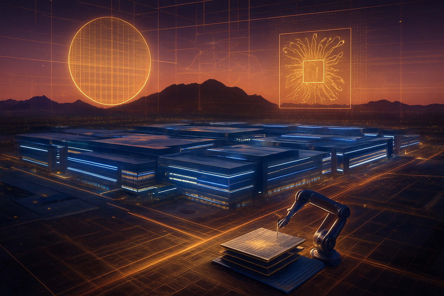
For Tower Semiconductor, the strategic benefits are equally transformative. The company has announced a $650 million capital expenditure plan to expand its SiPho capacity, including a $300 million expansion of its Migdal HaEmek hub. This investment positions Tower as a critical "arms dealer" in the AI space, moving it beyond its traditional roots in analog and RF chips. By mid-2026, Tower expects its photonics-related revenue to approach $1 billion annually, with data center applications accounting for nearly half of its total business.
This development also reinforces Intel’s position in the ecosystem. Even as Intel competes in the GPU space, its foundry relationship with Tower allows it to profit from the massive demand for NVIDIA-compatible infrastructure. The "capacity corridor" agreement demonstrates a new era of foundry cooperation where specialized players like Tower can leverage the massive infrastructure of giants like Intel to meet the sudden, explosive needs of the AI market.
Addressing the Global Power Crisis and the Memory Wall
The broader significance of 1.6T silicon photonics extends into the sustainability of AI development. As AI models reach trillions of parameters, the energy required to move data between memory and processors has begun to eclipse the energy used for the actual computation. Tower’s 1.6T SiPho transceivers offer a staggering 70% power saving compared to traditional electrical interconnects. In a world where data center expansion is increasingly limited by local power grid capacities, this efficiency gain is not just a benefit—it is a necessity for the survival of the industry.
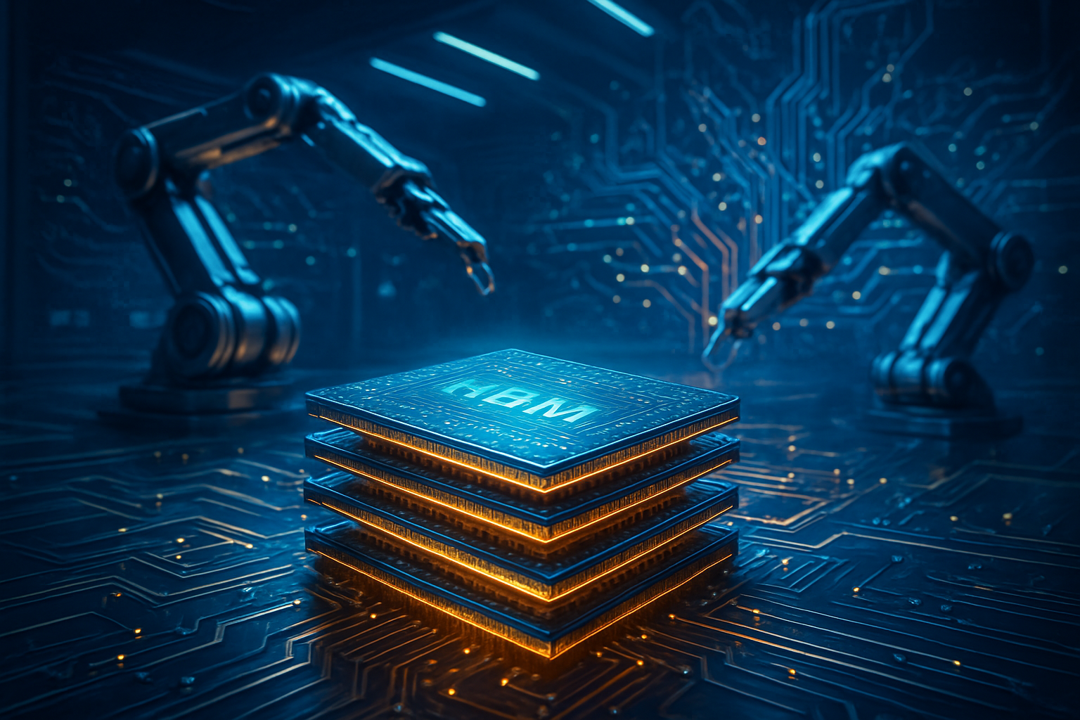
Beyond power, the "memory wall" has been the greatest hurdle to scaling AI. When GPUs have to wait for data to arrive from High Bandwidth Memory (HBM) or distant nodes, their utilization drops, wasting expensive compute cycles. Tower’s platform facilitates "disaggregated" architectures, where pools of memory and compute can be linked optically across a data center with such low latency that they behave as if they were on the same motherboard. This shift effectively "breaks" the memory wall, allowing for larger, more complex models that were previously impossible to train efficiently.
This milestone is often compared to the transition from copper telegraph wires to fiber optics in the 20th century. However, the stakes are higher and the pace is faster. The industry is moving from 400G to 1.6T in a fraction of the time it took to move from 10G to 100G, driven by a relentless "compute or die" mentality among the world’s leading technology companies.
The Road to 3.2T and Beyond
Looking ahead, the roadmap for Tower and its partners is already being drafted. By early 2026, Tower had already demonstrated 400G-per-lane modulators on its PH18DA platform, signaling that the leap to 3.2T solutions is already in sight. The industry expects to see the first 3.2T prototypes by late 2027, which will likely require even more advanced forms of Co-Packaged Optics and perhaps even monolithic integration of lasers directly onto the silicon.
Near-term developments will focus on the widespread adoption of CPO in "sovereign AI" clouds—nationalized data centers that prioritize energy independence and maximum throughput. We are also likely to see Tower’s SiPho technology bleed into other sectors, such as LIDAR for autonomous vehicles and quantum computing interconnects, where low-loss optical routing is equally vital. The challenge remains in the complexity of the assembly; "packaging" these light-based chips remains a highly specialized task that will require further innovation in automated OSAT (Outsourced Semiconductor Assembly and Test) flows.
A Turning Point for AI Infrastructure
Tower Semiconductor’s progress in 1.6T silicon photonics represents a definitive moment in the history of AI hardware. By solving the dual crises of bandwidth bottlenecks and power consumption, Tower and NVIDIA have cleared the path for the next generation of generative AI and autonomous systems. This is no longer just about making chips faster; it is about rethinking the very fabric of how information is moved and processed at a global scale.
In the coming weeks, the industry will be watching for the first benchmark results from NVIDIA’s 1.6T-enabled clusters. As these modules enter high-volume manufacturing, the impact on data center architecture will be profound. For investors and tech enthusiasts alike, the message is clear: the future of AI is not just in the silicon that thinks, but in the light that connects it.
This content is intended for informational purposes only and represents analysis of current AI developments.
TokenRing AI delivers enterprise-grade solutions for multi-agent AI workflow orchestration, AI-powered development tools, and seamless remote collaboration platforms.
For more information, visit https://www.tokenring.ai/.