Tag: AI Infrastructure

  • The Trillion-Parameter Workhorse: How NVIDIA’s Blackwell Architecture Redefined the AI Frontier

    The Trillion-Parameter Workhorse: How NVIDIA’s Blackwell Architecture Redefined the AI Frontier

    As of February 2, 2026, the artificial intelligence landscape has reached a pivotal milestone, driven largely by the massive industrial deployment of NVIDIA’s Blackwell architecture. What began as a bold promise in late 2024 has matured into the undisputed backbone of the global AI economy. The Blackwell platform, specifically the flagship GB200 NVL72, has bridged the gap between experimental large language models and the seamless, real-time "trillion-parameter" agents that now power enterprise decision-making and autonomous systems across the globe.

    The significance of the Blackwell era lies not just in its raw compute power, but in its fundamental shift from individual chips to "rack-scale" computing. By treating an entire liquid-cooled rack as a single, unified GPU, NVIDIA (NASDAQ: NVDA) has effectively bypassed the physical limits of silicon scaling. This architectural leap has provided the necessary overhead for the industry’s transition into Mixture-of-Experts (MoE) reasoning models, which require massive memory bandwidth and low-latency interconnects to function at the speeds required for human-like interaction.

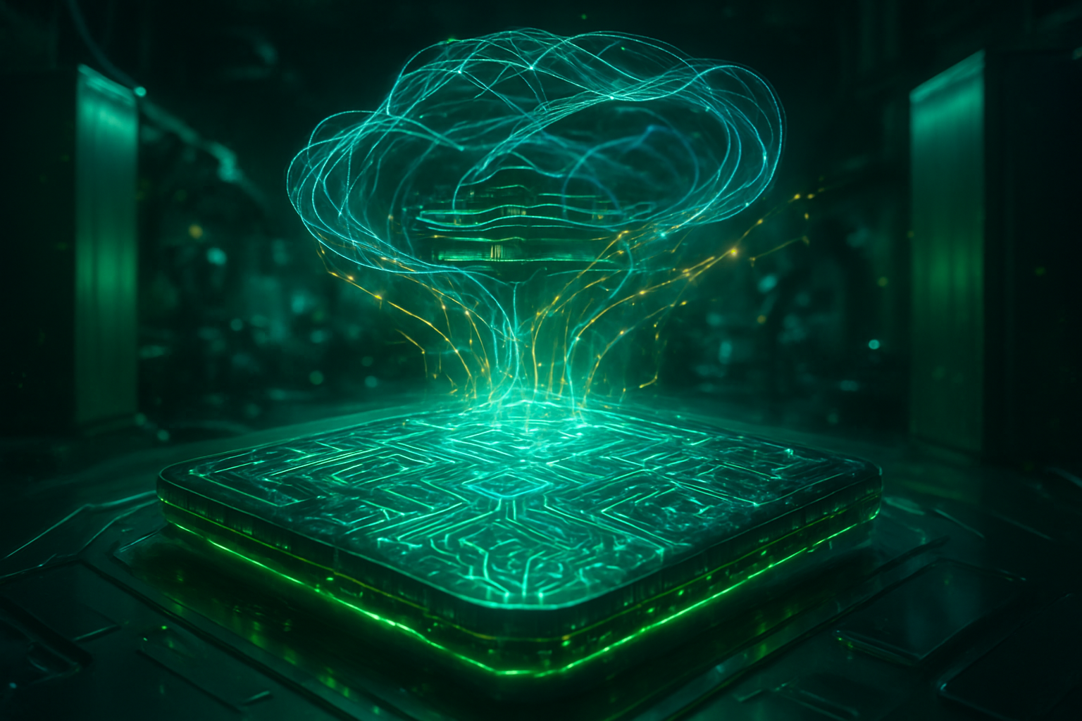
    Engineering the 130 Terabyte-per-Second "Giant GPU"

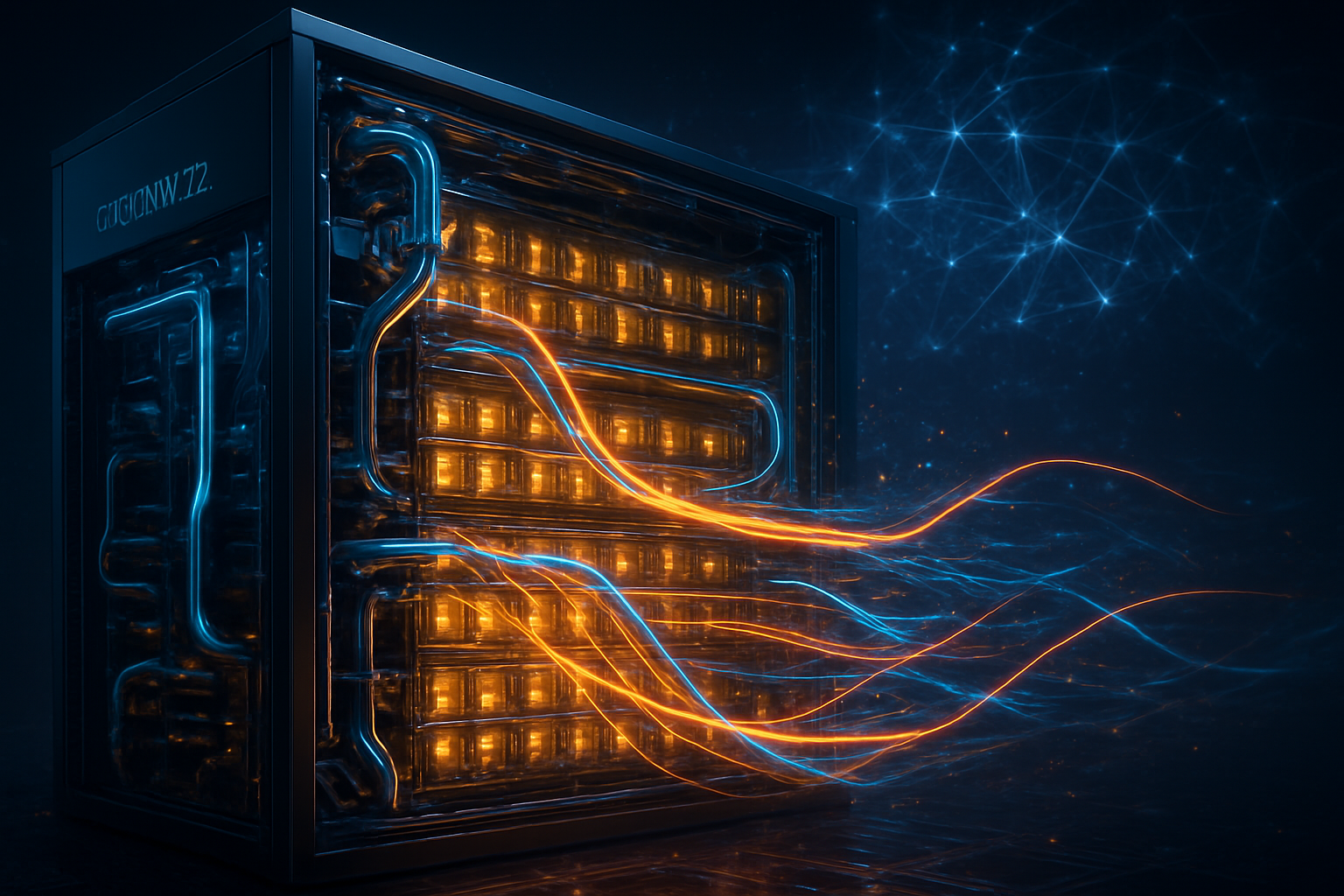
    At the heart of this technological dominance is the GB200 NVL72, a liquid-cooled system that interconnects 36 Grace CPUs and 72 Blackwell GPUs. The architectural innovation starts with the Blackwell chip itself, which utilizes a dual-die design with 208 billion transistors, linked by a 10 TB/s chip-to-chip interconnect. However, the true breakthrough is the fifth-generation NVLink, which provides a staggering 1,800 GB/s (1.8 TB/s) of bidirectional bandwidth per GPU. In the NVL72 configuration, this enables all 72 GPUs to communicate as one, creating an aggregate bandwidth domain of 130 TB/s—a feat that allows models with over 27 trillion parameters to be housed and processed within a single rack.

    This capability is specifically tuned for the complexities of Mixture-of-Experts (MoE) models. Unlike traditional dense models, MoE architectures rely on sparse activation, where only a subset of "experts" is triggered for any given task. The Blackwell architecture introduces a second-generation Transformer Engine and new FP4 (4-bit floating point) precision, which doubles throughput while maintaining the accuracy of larger models. Furthermore, a dedicated hardware decompression engine accelerates data movement by up to 800 GB/s, ensuring that the "experts" are swapped into memory with zero latency, resulting in a 30x improvement in real-time throughput for trillion-parameter models compared to the previous Hopper generation.

    Initial reactions from the AI research community have shifted from awe to total dependency. Leading researchers at labs like OpenAI and Anthropic have noted that without the NVLink 5 interconnect's ability to minimize "tail latency" during MoE inference, the current generation of multi-modal, agentic AI would have been financially and technically impossible to deploy at scale. The transition to liquid cooling has also been hailed as a necessary evolution, as the GB200 racks now handle power densities of up to 120kW, offering 25 times the energy efficiency of the air-cooled H100 systems that preceded them.

    The Hyperscaler Arms Race and Sovereign AI

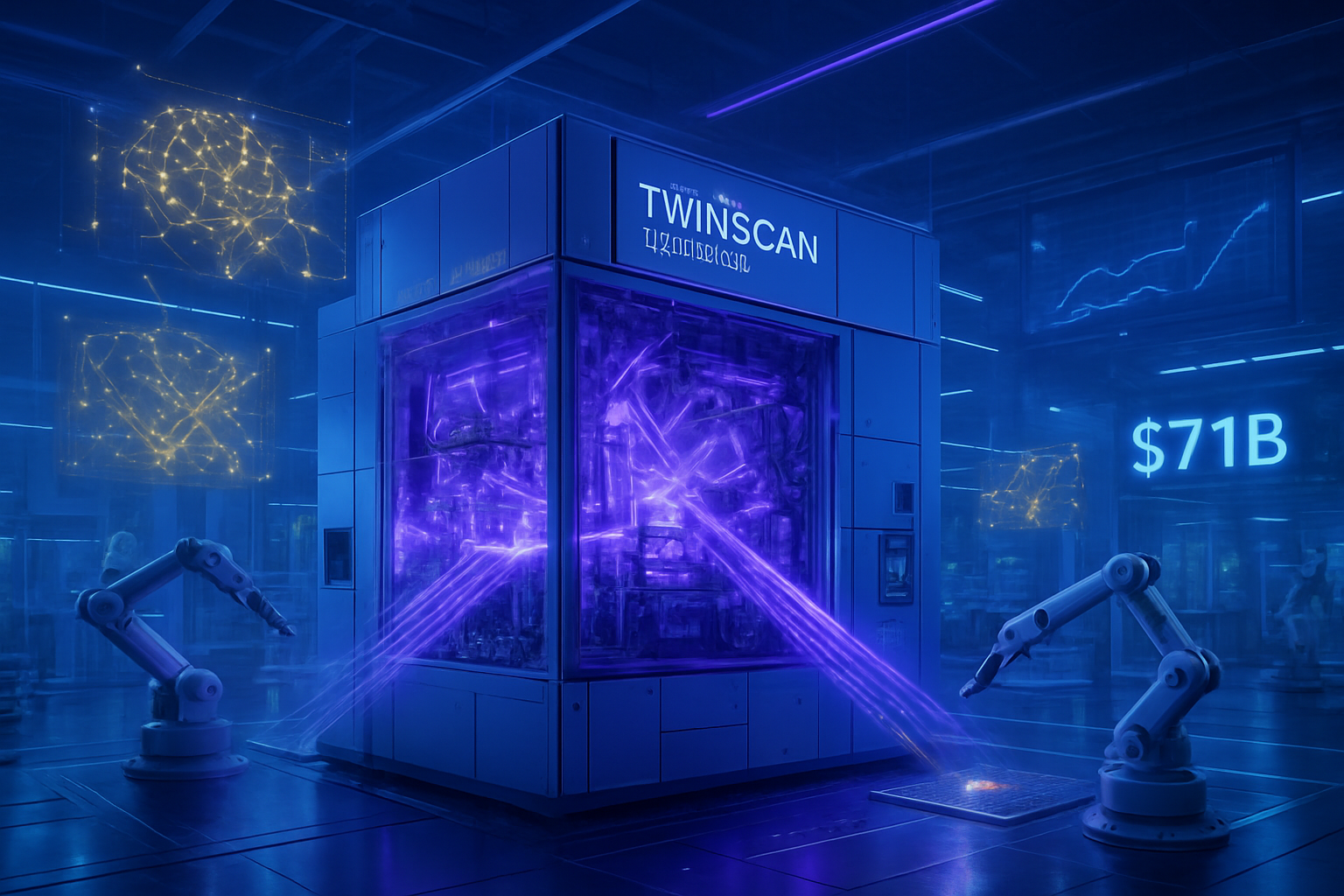
    The deployment of Blackwell has solidified a hierarchy among tech giants. Microsoft (NASDAQ: MSFT), Amazon (NASDAQ: AMZN), and Alphabet (NASDAQ: GOOGL) have engaged in a relentless race to secure the largest clusters of GB200 NVL72 racks. For these hyperscalers, the Blackwell architecture is more than just a performance upgrade; it is a strategic moat. By integrating Blackwell into their cloud infrastructure, these companies have been able to offer proprietary "AI Supercomputing" tiers that smaller competitors simply cannot match in terms of cost-per-token or training speed.

    Meta Platforms (NASDAQ: META) has also been a primary beneficiary, utilizing Blackwell to train and serve its Llama-4 and Llama-5 series. The ability of the NVL72 platform to handle massive MoE weights in-memory has allowed Meta to keep its open-source models competitive with closed-source offerings. Meanwhile, the emergence of "Sovereign AI"—where nations build their own domestic compute clusters—has seen countries like Saudi Arabia and Japan investing billions into Blackwell-based data centers to ensure their data and intelligence remain within their borders, further driving NVIDIA’s 90% market share in the AI accelerator space.

    The competitive implications extend beyond the chip makers. While Advanced Micro Devices (NASDAQ: AMD) has made significant strides with its Instinct MI400 series, NVIDIA’s "one-year cadence" strategy has kept rivals in a perpetual state of catch-up. Startups that built their software stacks on CUDA (NVIDIA’s parallel computing platform) are finding it increasingly difficult to switch to alternative hardware, as the optimizations for Blackwell’s FP4 and NVLink 5 are deeply integrated into the modern AI development lifecycle. This has created a "virtuous cycle" for NVIDIA, where its hardware dominance reinforces its software lock-in.

    Beyond the Transistor: A New Era of Compute Efficiency

    When viewed through the lens of the broader AI landscape, Blackwell represents the moment AI moved from "predictive text" to "active reasoning." The massive bandwidth provided by the 1,800 GB/s NVLink 5 links has solved the memory-wall problem that plagued earlier AI architectures. This has enabled the development of "agentic" systems—AI that doesn't just answer questions but can plan, execute, and monitor multi-step tasks across different software environments. The efficiency gains have also quieted some of the criticisms regarding AI's environmental impact; the 25x increase in energy efficiency means that while AI workloads have grown, the carbon footprint per inference has plummeted.

    However, this concentration of power has not been without concern. The sheer cost of a single GB200 NVL72 rack—estimated in the millions of dollars—has raised questions about the democratization of AI. There is a growing divide between the "compute-rich" and the "compute-poor," where only the top-tier corporations and nation-states can afford to train the next generation of frontier models. Comparisons are often made to the early days of the Manhattan Project or the Space Race, where the sheer scale of the infrastructure required dictates who the global power players will be.

    Despite these concerns, the impact of Blackwell on scientific research has been profound. In fields like drug discovery and climate modeling, the ability to run trillion-parameter simulations in real-time has accelerated breakthroughs that were previously decades away. The architecture has effectively turned the data center into a giant laboratory, capable of simulating complex molecular interactions or global weather patterns with a level of granularity that was unthinkable in the era of the H100.

    The Horizon: From Blackwell to Rubin

    As we look toward the latter half of 2026, the AI industry is already preparing for the next leap. NVIDIA has officially teased the "Rubin" architecture, slated for a late 2026 release. Rubin is expected to transition to a 3nm process and debut the "Vera" CPU, alongside the sixth-generation NVLink, which is rumored to double bandwidth again to 3.6 TB/s. The move to HBM4 memory will further expand the capacity of these machines to handle even more massive models, potentially pushing into the 100-trillion-parameter range.

    The near-term focus, however, remains on the refinement of Blackwell. Experts predict that the next 12 months will see a surge in "Edge Blackwell" applications, where the power of the architecture is condensed into smaller form factors for autonomous vehicles and robotics. The challenge will be managing the heat and power requirements of such high-density compute in mobile environments. Furthermore, as models become even more efficient through 4-bit and even 2-bit quantization, the software layer will need to evolve to keep pace with the hardware’s ability to process data at terabyte-per-second speeds.

    A Definitive Chapter in AI History

    NVIDIA’s Blackwell architecture will likely be remembered as the technology that industrialized artificial intelligence. By solving the interconnection bottleneck with the 1,800 GB/s NVLink and the GB200 NVL72 platform, NVIDIA did more than just release a faster chip; they redefined the unit of compute from the GPU to the data center rack. This shift has enabled the current era of trillion-parameter MoE models, providing the raw power necessary for AI to move into its reasoning and agentic phase.

    As we move further into 2026, the key developments to watch will be the first production deployments of the Rubin architecture and the continued expansion of Sovereign AI clusters. While the competition from custom hyperscaler chips and rival GPU makers continues to grow, the Blackwell platform’s integrated ecosystem of hardware, software, and networking remains the gold standard. For now, the "Blackwell Era" stands as the most significant period of compute expansion in human history, laying the foundation for whatever intelligence comes next.


    This content is intended for informational purposes only and represents analysis of current AI developments.

    TokenRing AI delivers enterprise-grade solutions for multi-agent AI workflow orchestration, AI-powered development tools, and seamless remote collaboration platforms.
    For more information, visit https://www.tokenring.ai/.

  • The Boiling Point: AI’s Liquid Cooling Era Begins as NVIDIA Rubin Pushes Data Centers to the Brink

    The Boiling Point: AI’s Liquid Cooling Era Begins as NVIDIA Rubin Pushes Data Centers to the Brink

    As of February 2, 2026, the artificial intelligence industry has officially reached its thermal breaking point. What was once a niche engineering challenge—cooling the massive compute clusters that power large language models—has become the primary bottleneck for the global expansion of AI. The transition from traditional air cooling to mainstream liquid cooling is no longer a strategic choice for data center operators; it is a physical necessity. With the recent debut of NVIDIA (NASDAQ: NVDA) Blackwell and the upcoming deployment of the Rubin architecture, the sheer density of heat generated by these silicon behemoths has rendered the fans and air-conditioning units of the past decade obsolete.

    This shift marks a fundamental transformation in the anatomy of the data center. For thirty years, the industry relied on "cold aisles" and high-powered fans to whisk away heat. However, as AI chips breach the 1,000-watt barrier per component, the physics of air—a notoriously poor conductor of heat—have failed. Today, the world’s largest cloud providers, including Microsoft (NASDAQ: MSFT), Amazon (NASDAQ: AMZN), and Alphabet (NASDAQ: GOOGL), are racing to retrofit existing facilities and construct massive "AI Superfactories" built entirely around liquid loops, signaling the most significant infrastructure overhaul in the history of modern computing.

    The Physics of Rubin: Why Air Finally Failed

    The technical requirements for the latest generation of AI hardware have shattered previous industry standards. While the NVIDIA Blackwell B200 GPUs, which dominated throughout 2025, pushed Thermal Design Power (TDP) to a staggering 1,200 watts per chip, the recently unveiled Rubin R100 platform has moved the goalposts even further. Early production units of the Rubin architecture, slated for volume shipment in the second half of 2026, are pushing individual GPU TDPs toward 2,000 watts. When these chips are clustered into the Vera Rubin NVL72 rack configuration, the power density reaches an eye-watering 140kW to 200kW per rack. To put this in perspective, a standard enterprise server rack just five years ago typically consumed between 5kW and 10kW.

    To manage this heat, the industry has standardized on Direct-to-Chip (DTC) cooling and, increasingly, immersion cooling. DTC technology uses "cold plates"—high-conductivity copper blocks—that sit directly atop the GPU and memory stacks. A dielectric or treated water-based fluid circulates through these plates, absorbing heat far more efficiently than air. The technical leap with the Rubin platform is its mandate for "warm water cooling." By utilizing liquid at 45°C (113°F), data centers can eliminate energy-intensive mechanical chillers, instead using simple dry coolers to dissipate heat into the ambient air. This breakthrough has allowed leading server manufacturers like Super Micro Computer (NASDAQ: SMCI) and Dell Technologies (NYSE: DELL) to design systems that are not only more powerful but significantly more energy-efficient, with some facilities reporting Power Usage Effectiveness (PUE) ratings as low as 1.05.

    The Infrastructure Gold Rush: Beneficiaries of the Liquid Shift

    The forced migration to liquid cooling has created a new class of high-growth infrastructure giants. Vertiv (NYSE: VRT) and Schneider Electric (OTCPK: SBGSY) have emerged as the primary "arms dealers" in this transition. Vertiv, in particular, has seen its market position solidify through its modular liquid-cooling units that can be rapidly deployed in existing data centers. Schneider Electric’s 2025 acquisition of Motivair has allowed it to offer end-to-end "liquid-ready" architectures, from the Cooling Distribution Units (CDUs) to the manifold systems that snake through the server racks.

    This transition has also created a competitive divide among colocation providers. Companies like Equinix (NASDAQ: EQIX) and Digital Realty (NYSE: DLR) that moved early to install heavy-duty piping and liquid-loop infrastructure are now the only facilities capable of hosting the next generation of AI training clusters. Smaller data center operators that failed to invest in liquid-ready footprints are finding themselves locked out of the lucrative AI market, as their facilities simply cannot provide the power density or cooling required for Blackwell or Rubin hardware. This infrastructure "moat" is reshaping the real estate dynamics of the tech industry, favoring those with the capital and engineering foresight to embrace a "wet" data center environment.

    Sustainability and the Global Power Paradigm

    Beyond the immediate technical hurdles, the adoption of liquid cooling is a double-edged sword for the environment. On one hand, liquid cooling is vastly more efficient than air cooling, potentially reducing a data center’s cooling-related energy consumption by up to 90%. This efficiency is critical as the total power demand of the AI sector is projected to rival that of small nations by the end of the decade. By moving to warm water cooling, operators can significantly lower their carbon footprint and water consumption, as traditional evaporative cooling towers are no longer strictly necessary.

    However, the sheer scale of the new AI Superfactories presents a daunting challenge. The move to liquid cooling allows for much higher density, which in turn encourages the construction of even larger facilities. We are now seeing the rise of "gigawatt-scale" data center campuses. Concerns are mounting among local governments and environmental groups regarding the massive localized power draw and the potential for "thermal pollution"—the release of massive amounts of waste heat into the environment. While the technology is more efficient per unit of compute, the total volume of compute is growing so rapidly that it may offset these gains, keeping the industry in a perpetual race against its own energy demands.

    The Road to 600kW: What Comes After Rubin?

    As we look toward 2027 and 2028, the trajectory of AI hardware suggests that even current liquid cooling methods may eventually reach their limits. Experts predict that the successor to Rubin, already whispered about in R&D circles, will likely push rack densities toward 600kW. At these levels, "phase-change" cooling—where the liquid refrigerant actually boils and turns to gas as it absorbs heat—is expected to become the new frontier. This technology, currently in testing by specialized firms like nVent (NYSE: NVT), promises an even greater step-change in thermal management.

    Furthermore, we are beginning to see the first practical applications of "district heating" from AI data centers. In northern Europe and parts of North America, the high-grade waste heat (reaching 60°C or more) from liquid-cooled AI clusters is being piped into local municipal heating systems to warm homes and businesses. This "circular heat" economy could transform data centers from energy sinks into valuable public utilities, providing a social and economic justification for their immense power consumption. The challenge will remain in the global supply chain, as the demand for specialized components like quick-disconnect manifolds and high-pressure pumps currently exceeds manufacturing capacity by nearly 40%.

    A Liquid Future for the Intelligence Age

    The mainstreaming of liquid cooling in early 2026 represents a pivotal moment in the history of computing. It is the point where the digital and the physical have collided most violently, forcing a total redesign of how we build the brains of the AI era. The transition driven by NVIDIA’s relentless release cycle—from Hopper to Blackwell and now to Rubin—has permanently altered the data center landscape. Air cooling, once the bedrock of the industry, is now a relic of a lower-density past, reserved for legacy workloads and basic enterprise tasks.

    As we move forward, the success of AI companies will be measured not just by their algorithms or their data, but by their thermal engineering. In the coming months, watch for the first full-scale deployments of "Vera Rubin" clusters and the quarterly earnings of infrastructure providers like Vertiv and Schneider Electric, which have become the barometers for AI’s physical growth. The era of the "cool and quiet" data center is over; the era of the high-density, liquid-powered AI factory has arrived.


    This content is intended for informational purposes only and represents analysis of current AI developments.

    TokenRing AI delivers enterprise-grade solutions for multi-agent AI workflow orchestration, AI-powered development tools, and seamless remote collaboration platforms.
    For more information, visit https://www.tokenring.ai/.

  • The Silicon Throne: TSMC’s Record $56B Bet on the Future of Artificial Intelligence

    The Silicon Throne: TSMC’s Record $56B Bet on the Future of Artificial Intelligence

    In a move that underscores the sheer scale of the ongoing generative artificial intelligence revolution, Taiwan Semiconductor Manufacturing Company (NYSE:TSM) has officially announced a record-breaking $56 billion capital expenditure plan for 2026. This historic investment, disclosed during the company’s recent Q1 earnings briefing, marks the largest single-year spending commitment in the history of the semiconductor industry. As the world’s leading foundry, TSMC is signaling its absolute confidence that the demand for high-performance computing (HPC) will continue to accelerate, fueled by the insatiable needs of AI hyperscalers and chip designers.

    The significance of this announcement extends far beyond simple infrastructure. TSMC has projected a massive 30% revenue growth for the fiscal year 2026, a figure that has sent shockwaves through global markets. By allocating over 80% of its budget to advanced nodes and specialized packaging, TSMC is not just building more factories; it is constructing the physical bedrock upon which the next decade of AI breakthroughs—including autonomous systems, massive-scale LLMs, and personalized digital agents—will be built.

    Scaling the Impossible: 2nm and the Rise of A16 Architecture

    The technical core of TSMC’s 2026 strategy lies in the aggressive ramp-up of its 2nm (N2) process and the introduction of the groundbreaking A16 (1.6nm) node. The N2 process, which is now hitting mass production across TSMC’s facilities in Baoshan and Kaohsiung, represents a paradigm shift in transistor design. For the first time, TSMC is utilizing Gate-All-Around (GAA) nanosheet transistors. Unlike the previous FinFET architecture, GAA allows for better electrostatic control, resulting in a 10-15% performance boost or a 25-30% reduction in power consumption compared to the 3nm node.

    Complementing the 2nm rollout is the A16 node, scheduled for volume production in the second half of 2026. The A16 is being hailed by industry experts as the "crown jewel" of TSMC’s roadmap because it introduces the "Super Power Rail." This backside power delivery system moves power distribution from the front of the wafer to the back, freeing up critical space on the top layers for signal routing. This technical leap effectively eliminates bottlenecks in power delivery that have plagued high-wattage AI accelerators, allowing for even higher clock speeds and more efficient thermal management.

    Initial reactions from the semiconductor research community suggest that TSMC has successfully widened its lead over rivals Intel (NASDAQ:INTC) and Samsung. While Intel has made strides with its 18A process, TSMC’s ability to achieve volume production with A16 while maintaining nearly 50% net margins is viewed as a masterstroke in manufacturing execution. "We are no longer just looking at incremental shrinks," said one senior analyst at the Semiconductor Industry Association. "TSMC is re-engineering the very physics of how electricity moves through a chip to meet the thermal demands of the AI era."

    The NVIDIA and Meta Connection: Powering the AI Super-Cycle

    This $56 billion investment is a direct response to the "AI Super-Cycle" led by tech giants like NVIDIA (NASDAQ:NVDA) and Meta (NASDAQ:META). NVIDIA, which has officially overtaken Apple (NASDAQ:AAPL) as TSMC’s largest customer, is the primary driver for the 2026 capacity surge. NVIDIA’s upcoming "Rubin" architecture, the successor to the Blackwell GPUs, is slated to transition to TSMC’s 3nm (N3P) and eventually 2nm nodes. To satisfy NVIDIA’s roadmap, TSMC is also doubling down on its CoWoS (Chip on Wafer on Substrate) advanced packaging capacity, which remains the primary bottleneck for shipping enough AI chips to meet global demand.

    Meta’s role in this expansion is equally pivotal. Mark Zuckerberg’s company has emerged as a top-tier TSMC client, securing massive allocations for its custom Meta Training and Inference Accelerator (MTIA) chips. As Meta continues its pivot toward "General AI" and integrates advanced intelligence across its social platforms, its reliance on bespoke silicon has made it a key strategic partner in TSMC’s long-term planning. For Meta, securing TSMC’s A16 capacity early is a competitive necessity to ensure its future models can out-compute rivals in a high-latency-sensitive environment.

    The market positioning here is clear: TSMC has created a "virtuous cycle" where the world’s most powerful software companies are effectively subsidizing the development of the world’s most advanced hardware. This creates a formidable barrier to entry for smaller firms and even legacy tech giants. Companies that do not have "priority access" to TSMC’s 2nm and A16 nodes in 2026 risk falling an entire generation behind in compute efficiency, which in the AI world translates directly to higher costs and slower innovation.

    Geopolitics and the Global Fab Cluster Strategy

    The $56 billion plan is not just about technology; it is about geographical resilience. TSMC is currently transforming its manufacturing footprint into "Megafab Clusters" located in the United States, Japan, and Germany. In Arizona, Fab 1 is now fully operational at the 4nm node, while the mass production timeline for Fab 2 has been accelerated to late 2027 to handle 3nm and 2nm chips. This expansion is critical for US-based partners like AMD (NASDAQ:AMD) and NVIDIA, who are increasingly under pressure to diversify their supply chains amidst ongoing geopolitical tensions in the Taiwan Strait.

    However, this global expansion brings its own set of challenges. Critics have pointed to the rising costs of manufacturing outside of Taiwan, where TSMC benefits from a highly specialized local ecosystem. To maintain its 30% revenue growth target, TSMC has had to implement "regional pricing" models, charging a premium for chips made in US-based fabs. Despite these costs, the "AI gold rush" has made customers willing to pay for the security of supply.

    Comparatively, this milestone echoes the early 2010s mobile revolution, but at a significantly larger scale. While the shift to smartphones redefined consumer tech, the current AI infrastructure build-out is fundamental to the entire global economy. The concern among some economists is the potential for an "over-investment" bubble; however, with TSMC’s order books for 2026 and 2027 already reported as "fully booked," the immediate threat appears to be a lack of capacity rather than a surplus.

    Looking Ahead: The Road to Sub-1nm

    As 2026 unfolds, the industry is already looking toward the next frontier. TSMC has hinted at a "1nm-class" node research phase, potentially designated as the A14 or A10, which will likely integrate even more exotic materials like carbon nanotubes or two-dimensional semiconductors. In the near term, the focus will remain on the successful integration of High-NA EUV (High Numerical Aperture Extreme Ultraviolet) lithography machines, which are essential for printing the incredibly fine features required for the A16 node.

    The primary challenges moving forward are no longer just about lithography. Power and water consumption for these mega-facilities have become significant political and environmental hurdles. In Taiwan, TSMC is investing heavily in water reclamation plants and renewable energy to ensure its 2nm ramp-up does not strain local resources. In Arizona, the focus is on building out a local talent pipeline of specialized engineers to staff the three planned facilities.

    Experts predict that by the end of 2026, the gap between TSMC and its competitors will be defined not just by transistor density, but by "system-level" integration. This involves 3D stacking of logic and memory (SoIC), which TSMC is rapidly scaling. The future of AI is moving toward "Silicon-as-a-Service," where TSMC provides the entire compute package—not just the chip.

    A New Era of Silicon Sovereignty

    TSMC’s $56 billion commitment for 2026 is a definitive statement that the AI era is still in its infancy. By betting nearly 30% of its projected revenue back into R&D and capital projects, the company is ensuring its role as the indispensable middleman of the digital age. The key takeaways for 2026 are clear: the transition to 2nm and A16 architecture is the new battlefield for AI supremacy, and NVIDIA and Meta have secured their positions at the front of the line.

    As we move through the coming months, the tech world will be watching the yield rates of the new A16 node and the progress of the Arizona Fab 2 construction. This investment represents more than just a business plan; it is the most expensive and complex engineering project in human history, designed to power the next generation of human intelligence. In the high-stakes game of semiconductor manufacturing, TSMC has just raised the stakes to an unprecedented level, and the rest of the world has no choice but to follow.


    This content is intended for informational purposes only and represents analysis of current AI developments.

    TokenRing AI delivers enterprise-grade solutions for multi-agent AI workflow orchestration, AI-powered development tools, and seamless remote collaboration platforms.
    For more information, visit https://www.tokenring.ai/.

  • NAND Flash Overtakes Mobile: Data Centers Drive New Storage Record

    NAND Flash Overtakes Mobile: Data Centers Drive New Storage Record

    In a seismic shift for the semiconductor industry, data center demand for high-performance NAND Flash memory has officially surpassed that of mobile devices for the first time in history. This milestone, reached in early 2026, marks the end of a fifteen-year era where the smartphone was the primary engine of the storage market. The "AI Supercycle" has fundamentally reconfigured the global supply chain, transforming NAND from a commodity component found in consumer gadgets into a high-stakes bottleneck for the world’s most powerful AI clusters.

    As hyperscale cloud providers and enterprise data centers race to scale their artificial intelligence capabilities, the demand for ultra-fast, high-capacity Solid State Drives (SSDs) has exploded. Reports from the first quarter of 2026 indicate that data center NAND consumption is now growing at a staggering compound annual rate of 40%. This surge is driven by the realization that massive GPU compute power is only as effective as the storage systems capable of feeding it data.

    The Technical Shift: Feeding the Beast

    The pivot toward data center dominance is rooted in the technical requirements of Large Language Model (LLM) training and "agentic" AI inference. While High Bandwidth Memory (HBM) handles the active processing within GPUs like those from NVIDIA (NASDAQ: NVDA), the sheer scale of modern datasets requires a massive secondary tier of fast storage. To prevent "starving" the GPUs, data centers are moving away from traditional Hard Disk Drives (HDDs) in favor of all-flash arrays.

    The current generation of AI-ready storage is defined by the commercial debut of PCIe 6.0 enterprise SSDs. These drives, such as the Samsung Electronics (KRX: 005930) PM1763, offer sequential read speeds of up to 32 GB/s—doubling the performance of the previous PCIe 5.0 standard. Furthermore, capacity limits are being shattered; SK Hynix (KRX: 000660) and its subsidiary Solidigm have begun high-volume shipping of 122TB and 128TB SSDs, providing the density required to house "data lakes" that span petabytes of information in a single server rack.

    Industry experts note that this shift is not just about raw speed but also about the "Memory Wall." In early 2026, NVIDIA introduced its Inference Context Memory Storage (ICMS) platform, which uses high-speed NAND as a dedicated layer to store and share "Key-Value" caches across GPU pods. This architecture allows AI models to handle context windows spanning millions of tokens by treating NAND as an extension of the GPU’s own memory, a feat previously thought impossible due to latency constraints.

    Market Impact and the "Sold-Out" Era

    The competitive landscape of the storage industry has been completely upended. Micron Technology (NASDAQ: MU) recently announced that its 2026 supply of enterprise-grade NAND is effectively "fully committed," meaning the company is sold out for the remainder of the year. This supply-demand imbalance has led to record-breaking price increases for enterprise SSDs, which have spiked over 50% in the last quarter alone.

    The recent structural reorganization of major players also reflects this new reality. Following its 2025 spinoff from its parent company, the newly independent SanDisk Corporation (NASDAQ: SNDK) has pivoted its entire strategy to prioritize "Ultra QLC" (Quad-Level Cell) storage for AI. By focusing on its "Stargate" controller architecture, SanDisk is targeting 512TB capacities by 2027, leaving the legacy HDD business to the remaining Western Digital Corporation (NASDAQ: WDC).

    For tech giants like Alphabet (NASDAQ: GOOGL) and Microsoft (NASDAQ: MSFT), securing a stable supply of NAND has become as critical as securing GPUs. The shift has forced a strategic advantage for companies with "captive" memory production, such as Samsung, which can prioritize its own high-margin enterprise SSDs over sales to external mobile manufacturers. This has left the smartphone market—once the "king" of NAND—scrambling for crumbs in a market now dominated by the needs of the cloud.

    Broader Significance: The Death of the HDD in the Data Center?

    This development signals a broader trend: the potential obsolescence of mechanical hard drives in high-end compute environments. While Western Digital continues to innovate in high-capacity HDDs for bulk "cold" storage, the "warm" and "hot" data layers required for AI are now almost exclusively flash-based. The energy efficiency of NAND is a major factor here; modern AI SSDs consume roughly 25 watts while delivering massive throughput, a 60% gain in efficiency over older models. For power-constrained data centers, this efficiency is the only way to scale without exceeding local grid capacities.

    Comparatively, this milestone is being likened to the transition from dial-up to broadband. In the same way that broadband enabled the modern internet, the move to a NAND-dominant data center infrastructure is enabling the shift from static AI models to dynamic, real-time AI agents. The ability to retrieve and process vast amounts of data in milliseconds is the foundation of the "Agentic Era" of 2026.

    Future Horizons: The Path to Petabyte Storage

    Looking ahead, the roadmap for NAND flash is focused on two fronts: capacity and integration. Researchers are already testing "3D NAND" stacks with over 400 layers, which will be necessary to reach the 1-petabyte SSD milestone by the end of the decade. Additionally, the integration of compute-in-storage—where the SSD itself performs basic data preprocessing before sending it to the GPU—is expected to become a standard feature by 2027.

    However, challenges remain. The intense heat generated by PCIe 6.0 drives requires advanced cooling solutions, and the industry is still grappling with the environmental impact of such rapid semiconductor turnover. Furthermore, as data center demand continues to outpace production capacity, the risk of a global "storage crunch" looms, which could potentially slow the rollout of new AI services if left unaddressed.

    Conclusion: A New Era of Infrastructure

    The transition of NAND Flash from a mobile-first to a data center-first market is a defining moment in the history of AI. It marks the point where the infrastructure for artificial intelligence moved beyond experimental clusters into the backbone of the global economy. The 40% annual growth in consumption is not just a statistic; it is a reflection of the sheer volume of data being harnessed to power the next generation of human-machine interaction.

    As we move through 2026, the industry will be watching closely for the first 256TB commercial deployments and the impact of PCIe 6.0 on real-world AI inference speeds. For now, one thing is clear: the era of the "smart" phone as the driver of innovation is over. We have entered the era of the "intelligent" data center.


    This content is intended for informational purposes only and represents analysis of current AI developments.

    TokenRing AI delivers enterprise-grade solutions for multi-agent AI workflow orchestration, AI-powered development tools, and seamless remote collaboration platforms.
    For more information, visit https://www.tokenring.ai/.

  • India Semiconductor Mission 2.0: The Push for 2nm Domestic Fabrication

    India Semiconductor Mission 2.0: The Push for 2nm Domestic Fabrication

    India has officially entered the next phase of its ambitious technological ascent with the launch of the India Semiconductor Mission (ISM) 2.0. Announced in early February 2026, this expanded strategy marks a pivot from foundational manufacturing to the absolute bleeding edge of semiconductor technology. By earmarking significant new capital for 2nm and 3nm process nodes, the Indian government is signaling its intent to move beyond "lagging-edge" legacy chips and compete directly with the world’s most advanced fabrication hubs in Taiwan, South Korea, and the United States.

    The timing of this announcement is pivotal. As of February 2, 2026, the global semiconductor supply chain remains under immense pressure to diversify away from geographic bottlenecks. ISM 2.0 aims to capitalize on this by leveraging a $250 billion electronics production ecosystem that has matured over the last five years. With the first "Made in India" chips from Micron Technology (NASDAQ: MU) beginning to hit the global market this month, the mission’s second phase provides a high-octane roadmap to transform the nation from a consumer of silicon into a primary global anchor for advanced logic and AI hardware.

    Technical Ambition: The Roadmap to 2nm and 3nm Dominance

    ISM 2.0 introduces a rigorous technical roadmap that shifts the focus from 28nm-to-90nm mature nodes toward the "moonshot" goal of domestic 3nm and 2nm fabrication. Under the new guidelines, the Indian government has established a timeline to achieve 3nm pilot production by 2032 and full-scale 2nm manufacturing by 2035. This transition requires a massive leap in lithographic capability, moving from the current Deep Ultraviolet (DUV) systems to Extreme Ultraviolet (EUV) lithography. To support this, ISM 2.0 includes a specialized "Equipment and Materials" sub-scheme with a budget of approximately $4.8 billion (₹40,000 crore) to incentivize the domestic production of high-purity chemicals, gases, and substrates required for such precise manufacturing.

    The technical specifications of these advanced nodes are critical for the next generation of AI and high-performance computing (HPC). By targeting 2nm, India is preparing for a future where Gate-All-Around (GAA) transistor architectures replace the current FinFET designs. Experts note that this shift is not merely about scaling down; it involves a fundamental reimagining of chip geometry to improve energy efficiency by up to 30% and performance by 15% compared to 3nm. The mission’s technical advisory board, comprising veterans from global giants, has emphasized that India’s path will involve "co-development" models, where domestic IP is created alongside international foundry partners to ensure a unique value proposition in the global market.

    Initial reactions from the semiconductor research community have been cautiously optimistic. While the jump to 2nm is historically difficult, the deployment of "Virtual Twin" software by Lam Research (NASDAQ: LRCX) in Indian training hubs has already begun to bear fruit. By simulating 3nm/2nm nanofabrication in a digital environment, India has managed to reduce the training time for its specialized workforce by nearly 40%. This human-capital-first approach is seen as a key differentiator, as it addresses the chronic global shortage of skilled cleanroom engineers.

    A $250 Billion Ecosystem: Corporate and Strategic Advantages

    The corporate landscape in India is rapidly realigning to meet the demands of ISM 2.0. Leading the charge is Tata Electronics, a subsidiary of the Tata Group (NSE: TATAMOTORS), which is currently installing advanced ASML (NASDAQ: ASML) lithography equipment at its Dholera "Mega-Fab" in Gujarat. In partnership with Powerchip Semiconductor Manufacturing Corp (PSMC) (TPE: 6770), Tata is aiming for "First Silicon" by late 2026. The ISM 2.0 expansion provides additional financial incentives for these players to accelerate their transition from 28nm to more advanced logic nodes, potentially shortening the timeline for 7nm and 5nm trials.

    Beyond the "Big Three" of logic fabrication, the mission is creating a robust environment for specialized players. Himax Technologies (NASDAQ: HIMX) has already deepened its partnership with local assemblers for AI-sensing products, while Renesas Electronics (TYO: 6723) and CG Power (NSE: CGPOWER) are scaling high-volume assembly and testing operations. The infusion of capital into the Design Linked Incentive (DLI) 2.0 scheme is also empowering over 50 domestic fabless startups. These companies are focusing on "Specialized Silicon," such as ultra-low-power Edge AI chips, which are essential for the burgeoning Internet of Things (IoT) and autonomous vehicle markets.

    Market analysts suggest that India’s strategic advantage lies in its "full-stack" approach. Unlike earlier attempts to build standalone fabs, ISM 2.0 integrates the entire value chain—from R&D and design to chemicals and assembly. This ecosystem approach reduces the risk for tech giants looking to diversify their manufacturing footprints. By offering a stable, subsidized, and technologically progressive environment, India is positioning itself as a resilient alternative to traditional hubs, offering a unique "China Plus One" strategy that is backed by real infrastructure rather than just policy promises.

    Global Geopolitics and the Resilient Supply Chain

    The broader significance of ISM 2.0 cannot be overstated in the context of the 2026 global landscape. As artificial intelligence becomes the primary driver of national power, control over the silicon that powers AI is now a matter of sovereign security. India’s push for 2nm domestic fabrication is a clear signal that it intends to be a rule-maker, not just a rule-taker, in the global tech order. This move aligns with the "Global Partnership on AI" goals, positioning India as a democratic and reliable node in a fragmented supply chain.

    However, the path is fraught with challenges. The geopolitical tension surrounding semiconductor technology has led to strict export controls on advanced lithography tools. India's success depends heavily on its diplomatic ability to maintain access to EUV technology from the Netherlands and the United States. Furthermore, the environmental impact of such advanced manufacturing—which requires immense amounts of ultra-pure water and electricity—remains a point of concern. ISM 2.0 addresses this by mandating "Green Fab" standards, requiring new facilities to source at least 40% of their power from renewable energy by 2030.

    Comparatively, this milestone echoes the early 2000s software boom in India, but with significantly higher stakes. While the software era made India the "Back Office of the World," the semiconductor mission aims to make it the "Machine Room of the World." The transition from bits to atoms represents a fundamental maturation of the Indian economy, moving up the value chain to capture the high margins associated with advanced intellectual property and precision manufacturing.

    The Horizon: What Lies Ahead for Indian Silicon

    Looking forward, the near-term focus will be the successful commissioning of the Micron and Tata facilities. By the end of 2026, we expect to see the first commercial shipments of Indian-assembled and tested HBM (High Bandwidth Memory) and logic chips. These will likely find their way into domestic 5G infrastructure and automotive systems before scaling to international consumer electronics. In the long term, the success of ISM 2.0 will be judged by its ability to attract a "Top 3" global foundry—such as Intel (NASDAQ: INTC) or Samsung (KRX: 005930)—to establish a leading-edge node on Indian soil.

    The challenges remaining include the ultra-consistency required for 2nm yields and the sheer capital intensity of maintaining a leading-edge roadmap. Experts predict that the government may need to further increase the financial outlay beyond the current $20 billion commitment as the 2030s approach. However, with the total electronics production already hitting the $250 billion mark as of this month, the economic momentum appears sufficient to carry these ambitions forward.

    Conclusion: A New Era of Indian Innovation

    The India Semiconductor Mission 2.0 represents a watershed moment in the history of global technology. By setting its sights on 2nm and 3nm fabrication, India is not just catching up; it is attempting to leapfrog into the future of computing. The integration of a $250 billion ecosystem with targeted government support creates a formidable platform for growth that could redefine global trade patterns for decades.

    As we watch the first silicon emerge from Indian fabs in the coming months, the significance of this development will only grow. For the global tech industry, the message is clear: the next chapter of the semiconductor story is being written in the cleanrooms of Gujarat, Karnataka, and Tamil Nadu. The world should keep a close eye on India’s progress toward the 2nm frontier, as it may well determine the balance of technological power in the late 2020s and beyond.


    This content is intended for informational purposes only and represents analysis of current AI and semiconductor developments.

    TokenRing AI delivers enterprise-grade solutions for multi-agent AI workflow orchestration, AI-powered development tools, and seamless remote collaboration platforms.
    For more information, visit https://www.tokenring.ai/.

  • NVIDIA Overtakes Apple as TSMC’s Top Customer: The Dawn of the AI Utility Phase

    NVIDIA Overtakes Apple as TSMC’s Top Customer: The Dawn of the AI Utility Phase

    In a watershed moment for the global semiconductor industry, NVIDIA (NASDAQ: NVDA) has officially surpassed Apple (NASDAQ: AAPL) to become the largest revenue contributor for Taiwan Semiconductor Manufacturing Company (TSMC) (NYSE: TSM). Financial data emerging in early 2026 reveals a tectonic shift in the foundry’s client hierarchy: NVIDIA is projected to generate approximately $33 billion in revenue for TSMC this year, accounting for 22% of the total, while Apple, the long-standing "alpha" customer, is expected to contribute $27 billion, or roughly 18%.

    This reversal marks the first time in over a decade that a company other than Apple has held the top spot at the world’s premier chipmaker. The development is more than just a corporate milestone; it signals a fundamental realignment of the global economy. For the past fifteen years, the semiconductor market was largely defined by the smartphone and consumer electronics boom led by Apple. Today, that mantle has passed to the builders of artificial intelligence infrastructure, marking the definitive arrival of the "AI era" in industrial manufacturing.

    The Architecture of Dominance: Blackwell, Rubin, and the CoWoS Bottleneck

    The primary catalyst for this revenue surge is the sheer physical and technical complexity of NVIDIA’s latest silicon architectures. Unlike consumer-grade chips found in iPhones or MacBooks, which are optimized for power efficiency and mass-market costs, NVIDIA’s high-end AI accelerators like the Blackwell Ultra (GB300) and the upcoming Vera Rubin (R100) platforms are massive, high-performance systems. These chips push the boundaries of "reticle size"—the maximum area a single chip can occupy on a wafer—often requiring multiple dies to be stitched together with extreme precision. This complexity allows TSMC to command significantly higher prices per wafer compared to the smaller, more streamlined A-series chips produced for Apple.

    A critical component of this revenue growth is TSMC’s Chip on Wafer on Substrate (CoWoS) packaging technology. As AI models demand faster data throughput, the "glue" that connects GPUs with High-Bandwidth Memory (HBM) has become the industry’s most valuable bottleneck. NVIDIA has reportedly secured nearly 60% of TSMC’s entire CoWoS capacity for 2026. This advanced packaging is a high-margin service that adds a substantial layer of revenue on top of traditional wafer fabrication. By late 2026, TSMC’s CoWoS capacity is expected to reach over 100,000 wafers per month to keep pace with NVIDIA’s relentless release cycle.

    Initial reactions from the semiconductor research community suggest that NVIDIA’s move to the top spot was inevitable given the massive die sizes of the Rubin architecture. Analysts note that while Apple still ships hundreds of millions more individual chips than NVIDIA, the "value-per-wafer" for an AI accelerator is orders of magnitude higher. Industry experts believe this creates a "priority lock" where NVIDIA now gets first access to TSMC's most advanced nodes, such as the upcoming 2nm (N2) process, a privilege previously reserved almost exclusively for Apple.

    Reshaping the Tech Titan Hierarchy

    This shift has profound implications for the competitive landscape of Big Tech. For years, Apple’s dominance at TSMC gave it a strategic "moat," ensuring its products had the most efficient processors on the market before anyone else. Now, with NVIDIA as the primary revenue driver, TSMC is increasingly incentivized to prioritize the high-performance computing (HPC) requirements of AI over the low-power requirements of mobile devices. This could potentially slow the pace of performance gains in consumer hardware while accelerating the capabilities of the data centers that power AI services.

    Major AI labs and cloud providers—including Microsoft (NASDAQ: MSFT), Amazon (NASDAQ: AMZN), and Alphabet (NASDAQ: GOOGL)—stand to benefit from this alignment, as NVIDIA’s primary status ensures a steady, albeit expensive, supply of the hardware needed to scale their generative AI products. However, the high cost of NVIDIA’s Rubin platform, which targets a 10x reduction in token generation costs, creates a high barrier to entry for smaller startups. These companies must now navigate a market where the "silicon tax" is increasingly paid to a single, dominant provider that sits at the top of the manufacturing food chain.

    The strategic advantage has clearly pivoted. NVIDIA's ability to command TSMC’s roadmap means the foundry is now optimizing its future factories for "big silicon" rather than "small silicon." This transition forces competitors like AMD (NASDAQ: AMD) to compete for the remaining advanced packaging capacity, potentially tightening the supply of rival AI chips and further cementing NVIDIA’s market positioning as the de facto gatekeeper of AI compute.

    Entering the 'Utility Phase' of the AI Cycle

    Market analysts are describing this period as the transition from the "Land Grab Phase" to the "Utility Phase" of the AI cycle. During 2023 and 2024, the industry saw a frantic, speculative rush to acquire any available GPUs to avoid being left behind. In 2026, the focus has shifted toward Return on Investment (ROI) and enterprise-wide productivity. AI is no longer a peripheral experiment; it has become a core utility, as essential to modern business as electricity or high-speed internet.

    The fact that NVIDIA has overtaken Apple—a company built on consumer desire—indicates that the AI cycle is now driven by industrial necessity. This stage of the cycle requires a drastic reduction in the cost of intelligence to remain sustainable. This is why the Rubin architecture is so significant; by focusing on slashing the cost per token, NVIDIA is making it economically viable for businesses to embed AI into every layer of their software stacks. It represents a move toward the commoditization of high-level reasoning.

    Comparatively, this milestone is being likened to the moment in the early 20th century when industrial power generation surpassed residential lighting as the primary driver of the electrical grid. The sheer scale of infrastructure being built suggests that we are move past the "hype" and into a decade-long deployment phase. While concerns about an "AI bubble" persist, the hard capital expenditures flowing from the world’s most valuable companies into TSMC’s foundries suggest a long-term commitment to this technological pivot.

    The Horizon: 2nm and Beyond

    Looking ahead, the next battleground will be the transition to the 2nm (N2) process node, expected to ramp up in late 2026 and 2027. Experts predict that NVIDIA will be the lead customer for this node, utilizing "GAAFET" (Gate-All-Around Field-Effect Transistor) technology to further increase the density of its Rubin-successor chips. The challenge will not just be fabrication, but the continued scaling of HBM and advanced packaging, which remain prone to yield issues and supply chain disruptions.

    In the near term, we can expect NVIDIA to push deeper into vertical integration, perhaps offering more tailored "AI factories" that include not just the chips, but the liquid cooling and networking stacks required to run them. The goal is to move from selling components to selling entire units of "intelligence." Challenges remain, particularly regarding the massive power consumption of these new data centers and the geopolitical tensions surrounding semiconductor manufacturing in the Taiwan Strait, which remains a singular point of failure for the global AI economy.

    A New Era in Computing History

    The ascension of NVIDIA to the top of TSMC’s customer list is a historic realignment that marks the end of the mobile-first era and the beginning of the AI-first era. It underscores a shift in value from the device in our pockets to the massive, distributed intelligence engines in the cloud. NVIDIA’s $33 billion contribution to TSMC’s coffers is the ultimate proof of the industry's belief in the permanence of the AI revolution.

    As we move through 2026, the key metrics to watch will be the "cost-per-token" metrics provided by the Rubin platform and the speed at which TSMC can expand its CoWoS capacity. If NVIDIA can continue to lower the cost of AI while maintaining its lead at the foundry, it will solidify its role as the foundational utility of the 21st century. The world is no longer just buying gadgets; it is building a new kind of cognitive infrastructure, and for the first time, the numbers at the world's most important factory prove it.


    This content is intended for informational purposes only and represents analysis of current AI developments.

    TokenRing AI delivers enterprise-grade solutions for multi-agent AI workflow orchestration, AI-powered development tools, and seamless remote collaboration platforms.
    For more information, visit https://www.tokenring.ai/.

  • Foundation for the AI Era: Texas Instruments Commences Volume Production at $60 Billion SM1 ‘Mega-Fab’ in Sherman, Texas

    Foundation for the AI Era: Texas Instruments Commences Volume Production at $60 Billion SM1 ‘Mega-Fab’ in Sherman, Texas

    In a landmark moment for the American semiconductor industry, Texas Instruments (NASDAQ: TXN) has officially commenced volume production at its state-of-the-art SM1 fab in Sherman, Texas. The facility, which began shipping its first 300mm wafers to customers in late December 2025, represents the first phase of a massive $60 billion investment strategy aimed at securing the United States' lead in the foundational chips that power the artificial intelligence (AI) revolution, automotive autonomy, and industrial automation.

    The opening of SM1 marks a decisive shift in the global supply chain, moving the production of critical analog and embedded processing chips back to North American soil. While high-end GPUs often dominate the headlines, the chips produced at the Sherman "mega-site" serve as the essential nervous system and power management core for the world’s most advanced AI systems. As of January 30, 2026, the facility is operating ahead of schedule, reinforcing Texas Instruments' position as a dominant force in the high-growth industrial and automotive sectors.

    The 300mm Advantage: Engineering the Future of Edge AI

    The SM1 fab is specifically engineered for 300mm (12-inch) wafer production, a significant technological leap over the older 200mm lines common in the analog chip industry. By utilizing larger wafers, Texas Instruments can produce more than double the number of chips per wafer, drastically reducing costs and improving manufacturing efficiency. The facility focuses on 28nm to 130nm specialty process nodes—the "sweet spot" for analog and embedded chips that require high reliability and long lifecycles.

    Beyond the raw hardware, the Sherman site is a pioneer in "building AI with AI." The facility is one of the most automated in the world, featuring fully integrated material handling systems and the recent deployment of humanoid robots—specifically the UBTECH Walker S2—to manage repetitive tasks within the cleanroom. This AI-driven manufacturing environment generates terabytes of data every hour, which is processed in real-time to optimize wafer yields and perform predictive maintenance on sensitive lithography equipment. Initial reactions from industry analysts suggest that TI’s yields at SM1 are already exceeding industry benchmarks for a new fab, a testament to the facility's advanced automation.

    Strategic Dominance: How TI’s Expansion Reshapes the Tech Hierarchy

    The start of production at SM1 provides Texas Instruments with a significant competitive advantage over rivals like Analog Devices (NASDAQ: ADI) and Microchip Technology (NASDAQ: MCHP). By owning and operating its entire manufacturing flow—from wafer fabrication to assembly and test—TI can offer unparalleled supply chain transparency. This "capacity ahead of demand" strategy is designed to prevent the types of shortages that crippled the automotive industry in 2021, positioning TI as the preferred partner for tech giants and industrial leaders.

    Major beneficiaries of the Sherman expansion include companies at the forefront of the AI and automotive sectors. NVIDIA (NASDAQ: NVDA) and AMD (NASDAQ: AMD) rely on TI’s high-performance power management ICs (PMICs) to regulate the extreme energy requirements of their AI data center accelerators. Similarly, Ford (NYSE: F) and other EV manufacturers are utilizing the SM1-produced chips for advanced driver-assistance systems (ADAS) and 4D imaging radar. By providing a dependable, U.S.-sourced supply of these components, TI is effectively insulating its partners from the geopolitical risks associated with offshore manufacturing.

    Beyond the Silicon: The Broader Implications for National Security and AI

    The Sherman mega-site is more than just a factory; it is a cornerstone of the U.S. strategy to regain semiconductor sovereignty. Supported by the CHIPS and Science Act, which provided nearly $1.6 billion in direct funding, the $60 billion investment in Sherman and other U.S. sites (including Richardson and Lehi) represents a "moonshot" for American manufacturing. The project directly addresses the vulnerabilities of the global supply chain, ensuring that the "foundational" chips required for everything from Medtronic (NYSE: MDT) medical devices to SpaceX navigation systems remain available during international crises.

    In the broader context of the AI landscape, the SM1 fab is the catalyst for the transition from "Cloud AI" to "Edge AI." By mass-producing chips like the Sitara™ AM69A, which can perform complex computer vision tasks at extremely low power, TI is enabling the next generation of autonomous mobile robots and smart infrastructure. Experts believe this development is as significant as the breakthroughs in large language models, as it provides the physical infrastructure necessary for AI to interact with and navigate the real world.

    The Road Ahead: Scaling the Sherman Mega-Site

    While SM1 is now operational, it is only the beginning of Texas Instruments’ long-term vision. The Sherman campus is designed to house four total fabs (SM1 through SM4), with the exterior shell of SM2 already complete. As market demand for industrial and automotive electronics continues to rise, TI has the flexibility to equip and activate these additional facilities rapidly. Future upgrades are expected to focus on even tighter integration of AI within the fabrication process, potentially using machine learning to customize chip performance at the wafer level for specific client applications.

    In the near term, the industry will be watching the ramp-up of the SM2 facility and the further integration of humanoid robotics into the production workflow. Challenges remain, particularly in scaling the workforce to support four massive fabs simultaneously, but TI’s early success with SM1 suggests a clear path forward. Predictions from semiconductor analysts indicate that by 2030, the Sherman site could account for nearly 20% of the world’s 300mm analog chip production capacity.

    Conclusion: A New Era for American Semiconductors

    The start of production at TI’s SM1 fab marks a pivotal chapter in the history of American technology. By combining a $60 billion investment with cutting-edge AI-driven manufacturing, Texas Instruments has not only secured its own future but has also fortified the supply chains that the entire global economy depends on. The facility represents a triumphant return to domestic high-volume manufacturing, proving that the U.S. can compete on both innovation and scale.

    As we move into 2026, the success of the Sherman site will be a primary indicator of the health of the broader semiconductor industry. For investors and tech enthusiasts alike, the key takeaway is clear: while the software of AI captures our imagination, it is the precision-engineered silicon from fabs like SM1 that makes the revolution possible. Watch for upcoming announcements regarding the equipment of SM2 and further partnership agreements with Tier 1 automotive suppliers in the coming months.


    This content is intended for informational purposes only and represents analysis of current AI and semiconductor developments.

    TokenRing AI delivers enterprise-grade solutions for multi-agent AI workflow orchestration, AI-powered development tools, and seamless remote collaboration platforms.
    For more information, visit https://www.tokenring.ai/.

  • Micron Breaks Ground on $24 Billion ‘Double-Story’ Megafab in Singapore to Combat Global NAND Crisis

    Micron Breaks Ground on $24 Billion ‘Double-Story’ Megafab in Singapore to Combat Global NAND Crisis

    In a bold move to resolve the structural supply bottlenecks paralyzing the global artificial intelligence sector, Micron Technology (NASDAQ:MU) officially broke ground on its massive $24 billion (S$30.5 billion) NAND fabrication facility expansion in Singapore on January 27, 2026. This landmark investment, the largest in the company’s history within the region, aims to quintuple down on the memory requirements of the generative AI era. As the current "storage wall" continues to delay the deployment of high-capacity AI clusters worldwide, the groundbreaking marks a critical turning point for an industry grappling with a severe deficit of high-performance flash memory.

    The ceremony, held at Micron’s existing manufacturing hub in Woodlands, signals the start of a decade-long capital expenditure plan. By expanding its Singapore footprint, Micron is not just building more space; it is re-engineering the very architecture of semiconductor manufacturing to meet the insatiable appetite of data centers. With production slated for the second half of 2028, this facility is positioned as the primary global engine for the next generation of 3D NAND technology, specifically tailored for the high-density storage needs of AI inference models and autonomous systems.

    The 'Double-Story' Revolution: Engineering the Future of Flash

    The centerpiece of this announcement is the facility's unique architectural approach: it will be Singapore’s first "double-story" wafer fabrication plant. This multi-level design is a strategic response to the extreme land constraints of the city-state, allowing Micron to effectively double its production density without expanding its physical footprint horizontally. The new fab will add a staggering 700,000 square feet of cleanroom space—a 50% increase over Micron’s current local capacity. This vertical integration is a departure from traditional single-level layouts and represents a high-stakes engineering feat designed to maximize throughput per square meter.

    Technically, the facility is being optimized for the production of ultra-high-layer-count 3D NAND. While current industry standards are pushing past 300 layers, the 2028 production window suggests this fab will likely pioneer the transition toward 400-layer and 500-layer architectures. These advancements are essential for the enterprise-grade solid-state drives (SSDs) that power AI inference. Industry experts note that the double-story design also allows for more sophisticated material handling systems and automated overhead transport (OHT) systems that can operate across levels, reducing the latency between different stages of the lithography and etching processes.

    Initial reactions from the semiconductor research community have been overwhelmingly positive, though tempered by the reality of the timeline. Analysts at Gartner and IDC have praised Micron's foresight in securing long-term capacity, noting that the sheer scale of the 700,000-square-foot expansion is necessary to avoid a permanent state of shortage. However, some researchers point out that the complexity of a multi-story cleanroom environment poses significant vibration-control challenges, which Micron must overcome to maintain the nanometer-scale precision required for advanced 3D NAND stacking.

    Shifting the Competitive Balance in the Memory Market

    The $24 billion expansion significantly alters the competitive landscape between Micron and its primary rivals, Samsung Electronics (KRX:005930) and SK Hynix (KRX:000660). Throughout 2025, both Samsung and SK Hynix aggressively pivoted their manufacturing lines away from NAND to prioritize High Bandwidth Memory (HBM) and DDR5 DRAM, which were deemed more profitable during the initial AI training gold rush. This pivot inadvertently created a massive void in the NAND market. Micron’s massive commitment to NAND in Singapore allows it to capture this neglected market share, positioning the company as the primary supplier for the "Inference Boom" that follows the current "Training Boom."

    Hyperscale cloud providers—including Amazon, Google, and Microsoft—stand to benefit most from this development. These tech giants have faced lead times for enterprise SSDs exceeding 52 weeks in late 2025, a delay that has stalled the expansion of AI-driven consumer services. By establishing a dedicated "Center of Excellence" for NAND in Singapore, Micron provides these companies with a roadmap for reliable, high-volume supply. This move also puts pressure on competitors to announce similar capacity expansions or risk losing their standing in the lucrative data center storage segment.

    The strategic advantage for Micron lies in its geographical diversification. While its competitors are heavily concentrated in South Korea, Micron’s deepening roots in Singapore provide a stable, neutral manufacturing base that is less susceptible to regional geopolitical tensions. This has made Micron an increasingly attractive partner for Western tech firms looking to de-risk their supply chains while maintaining access to the cutting edge of memory technology.

    The 'Storage Wall' and the Shift to AI Inference

    This development fits into a broader shift in the AI landscape: the transition from model training to large-scale inference. While the industry’s focus was previously on the GPUs and HBM needed to build models like GPT-5 and its successors, the focus has now shifted to the storage needed to run them efficiently. AI inference requires massive datasets to be accessed nearly instantaneously, making traditional hard-disk drives (HDDs) obsolete in the modern data center. The global NAND supply crisis of 2025–2026 has exposed a "storage wall," where AI performance is no longer limited by compute power, but by the speed and capacity of the data retrieval layer.

    The environmental impact of this expansion is also a point of discussion. Modern AI data centers are massive energy consumers; however, transitioning from HDDs to the ultra-high-density SSDs produced by Micron’s new fab can reduce data center power consumption for storage by up to 70%. Micron has committed to ensuring the new Singapore facility meets high sustainability standards, utilizing advanced water recycling and energy-efficient climate control systems for its massive cleanrooms.

    Comparisons are already being drawn between this groundbreaking and the 2022 CHIPS Act announcements in the United States. While those focused on domestic logic and DRAM, the Singapore expansion is being viewed as the "missing piece" of the AI infrastructure puzzle. Without this NAND capacity, the trillions of dollars invested in AI compute would remain underutilized, effectively bottlenecked by slow data access.

    The Road to 2028: What Lies Ahead

    Looking forward, the immediate challenge remains the "supply gap" between now and the 2028 operational date. Experts predict that NAND prices will remain volatile through 2026 and 2027 as existing facilities operate at 100% capacity. In the interim, Micron is expected to implement "brownfield" upgrades to its current Singapore fabs to squeeze out incremental gains while the new double-story structure rises. Once online in 2028, the facility will not only serve data centers but will also be instrumental in the rollout of humanoid robotics and sophisticated autonomous vehicle fleets, both of which require terabytes of local, high-speed NAND storage.

    The next two years will likely see Micron and its peers experimenting with "PLC" (Penta-Level Cell) NAND technology and further advancements in string stacking. The success of the Singapore fab will depend on Micron's ability to maintain high yields on these increasingly complex architectures. Furthermore, as AI models move toward "World Models" that process video and 3D spatial data in real-time, the demand for 100TB and 200TB enterprise SSDs will become the new industry standard, a target Micron is now well-positioned to hit.

    A New Pillar for the AI Era

    Micron's $24 billion investment is more than a capacity expansion; it is a foundational pillar for the next decade of computing. By breaking ground on a facility of this scale during a global supply crisis, Micron has sent a clear signal to the market: storage is no longer a secondary concern to compute. The "double-story" fab represents a triumph of engineering and a strategic masterstroke that addresses the physical and economic constraints of modern semiconductor manufacturing.

    As we move toward 2028, the industry will be watching the Woodlands site closely. The success of this project will likely dictate the pace at which AI can be integrated into everyday technology, from edge devices to global cloud networks. For now, the groundbreaking serves as a vital promise of relief for a supply-starved industry and a testament to Singapore's enduring role as a central nervous system for the global tech economy.


    This content is intended for informational purposes only and represents analysis of current AI developments.

    TokenRing AI delivers enterprise-grade solutions for multi-agent AI workflow orchestration, AI-powered development tools, and seamless remote collaboration platforms.
    For more information, visit https://www.tokenring.ai/.

  • ASML’s $71 Billion Ambition: The High-NA EUV Revolution Powering the AI Era

    ASML’s $71 Billion Ambition: The High-NA EUV Revolution Powering the AI Era

    In a definitive signal of the semiconductor industry’s direction, ASML (NASDAQ: ASML) has solidified its 2030 revenue target at a staggering $71 billion (€60 billion), underpinned by the aggressive rollout of its High-NA (Numerical Aperture) EUV lithography systems. This announcement comes as the Dutch technology giant marks a historic milestone: the successful delivery and installation of the first commercial-grade TWINSCAN EXE:5200B systems to industry leaders Intel (NASDAQ: INTC) and SK Hynix (KRX: 000660). As of January 30, 2026, ASML stands at the center of the global AI arms race, with its order backlog swelling to record levels as chipmakers scramble for the tools necessary to manufacture the next generation of AI accelerators and high-bandwidth memory.

    The transition to High-NA EUV represents more than just an incremental upgrade; it is a fundamental shift in how the world’s most advanced silicon is produced. Driven by an insatiable demand for AI-capable hardware, ASML’s roadmap now bridges the gap between today’s 3-nanometer processes and the upcoming "Angstrom era." With its recent quarterly bookings nearly doubling analyst expectations, ASML has transformed from a equipment supplier into the ultimate gatekeeper of the AI economy, ensuring that the hardware requirements of generative AI models can be met through unprecedented transistor density and energy efficiency.

    The Technical Leap: Decoding the EXE:5200B

    The core of ASML’s growth strategy lies in the TWINSCAN EXE:5200B, the company’s first "production-worthy" High-NA system. Unlike the previous standard EUV (Low-NA) machines that utilized a 0.33 numerical aperture, the EXE:5200B jumps to 0.55 NA. This technical shift allows for a resolution of just 8nm, a significant improvement over the 13nm limit of previous systems. This leap enables a 2.9x increase in transistor density, allowing engineers to pack nearly three times as many components into the same silicon footprint. For the AI research community, this means the potential for dramatically more powerful NPUs (Neural Processing Units) and GPUs that can handle trillions of parameters with lower power consumption.

    The most critical advantage of the EXE:5200B is its ability to perform "single-exposure" lithography for features that previously required complex multi-patterning techniques. Multi-patterning—essentially passing a wafer through a machine multiple times to etch a single layer—is notorious for increasing defects and manufacturing cycle times. By achieving these fine details in a single pass, High-NA EUV significantly reduces the complexity of 2nm and 1.4nm (Intel 14A) process nodes. Initial feedback from engineers at Intel's Oregon facility suggests that the 0.7nm overlay accuracy of the 5200B is providing the precision necessary to align the dozens of layers required for modern 3D transistor architectures, such as Gate-All-Around (GAA) FETs.

    Reshaping the Competitive Landscape

    The early delivery of these systems has already begun to shift the strategic balance among the world's leading chipmakers. Intel (NASDAQ: INTC) has moved aggressively to reclaim its "process leadership" crown, being the first to complete acceptance testing of the EXE:5200B in late 2025. By integrating High-NA early, Intel aims to bypass the mid-generation struggles of its competitors, targeting risk production of its 14A node by 2027. This move is seen as a high-stakes bet to draw major AI clients away from TSMC (NYSE: TSM), which has taken a more cautious, "fast-follower" approach to High-NA adoption due to the machine's estimated $380 million price tag.

    In the memory sector, the arrival of the EXE:5200B at SK Hynix (KRX: 000660) and Samsung Electronics (KRX: 005930) marks a pivotal moment for AI infrastructure. For the first time in ASML’s history, memory chip orders have surpassed logic orders, accounting for 56% of the company's recent bookings. This is directly attributable to the High-Bandwidth Memory (HBM) required by Nvidia (NASDAQ: NVDA) and other AI accelerator designers. HBM4 and HBM5 require the ultra-fine resolution of High-NA to manage the vertical stacking of memory layers and the high-speed interconnects that prevent data bottlenecks in large language model (LLM) training.

    The Broader Significance: Moore’s Law in the AI Age

    The $71 billion revenue target is a testament to the fact that "lithography intensity" is increasing. As chips become more complex, they require more EUV exposures per wafer. This trend effectively extends the life of Moore's Law, which many critics had pronounced dead a decade ago. By providing a path to the 1.4nm and 1nm nodes, ASML is ensuring that the hardware side of the AI revolution does not hit a scaling wall. The ability to print features at the angstrom level is the only way to keep up with the computational demands of future "Agentic AI" systems that will require real-time processing at the edge.

    However, ASML’s dominance also highlights a growing concern regarding industry concentration. With a record backlog of €38.8 billion ($46.3 billion), the entire global tech sector is now dependent on a single company’s ability to manufacture and ship these massive, school-bus-sized machines. Any supply chain disruption or geopolitical tension—particularly concerning export controls to China—could have immediate, cascading effects on the availability of AI compute. The sheer cost and complexity of High-NA EUV are creating a "Rich-Club" of chipmakers, potentially pricing out smaller players and consolidating the power of the "Big Three" (Intel, TSMC, and Samsung).

    The Road to 2030 and Beyond

    Looking ahead, ASML is already laying the groundwork for life after High-NA. While the EXE:5200B is expected to be the workhorse of the late 2020s, the company has begun exploring "Hyper-NA" lithography, which would push numerical apertures beyond 0.75. Near-term, the focus remains on ramping up the production of the 5200B to meet the massive orders scheduled for 2026 and 2027. Experts predict that as the software side of AI matures, the demand for specialized, custom silicon (ASICs) will explode, further driving the need for the flexible, high-precision manufacturing that High-NA provides.

    The challenges remain formidable. Each High-NA machine requires 250 crates and multiple cargo planes to transport, and the energy consumption of these tools is significant. ASML and its partners are under pressure to improve the sustainability of the lithography process, even as they push the limits of physics. As we move toward 2030, the integration of AI-driven "computational lithography"—where AI models predict and correct for optical distortions in real-time—will likely become as important as the physical lenses themselves.

    A New Chapter in Silicon History

    ASML’s journey toward its $71 billion goal is more than a financial success story; it is the heartbeat of modern technological progress. By successfully delivering the EXE:5200B to Intel and SK Hynix, ASML has proven that it can translate theoretical physics into a reliable industrial process. The massive backlog and the shift toward memory-heavy orders confirm that the AI boom is not a fleeting trend, but a structural shift in the global economy that requires a fundamental reimagining of semiconductor manufacturing.

    In the coming weeks and months, the industry will be watching the yields of the first High-NA-produced wafers. If Intel and SK Hynix can demonstrate a significant performance-per-watt advantage over standard EUV, the pressure on TSMC and other foundry players to accelerate their High-NA adoption will become unbearable. For now, ASML remains the indispensable architect of the digital future, holding the keys to the most advanced tools ever created by humanity.


    This content is intended for informational purposes only and represents analysis of current AI developments.

    TokenRing AI delivers enterprise-grade solutions for multi-agent AI workflow orchestration, AI-powered development tools, and seamless remote collaboration platforms.
    For more information, visit https://www.tokenring.ai/.

  • NVIDIA Shatters Records with $57B Quarterly Revenue as Blackwell Ultra Demand Reaches “Off the Charts” Levels

    NVIDIA Shatters Records with $57B Quarterly Revenue as Blackwell Ultra Demand Reaches “Off the Charts” Levels

    In a financial performance that has stunned even the most bullish Wall Street analysts, NVIDIA (NASDAQ: NVDA) has reported a staggering $57 billion in revenue for the third quarter of its fiscal year 2026. This milestone, primarily driven by a 66% year-over-year surge in its Data Center division, underscores an insatiable global appetite for artificial intelligence compute. CEO Jensen Huang described the current market environment as having demand that is "off the charts," as the world’s largest tech entities and specialized AI cloud providers race to secure the latest Blackwell Ultra architecture.

    The immediate significance of this development cannot be overstated. As of January 30, 2026, NVIDIA has effectively solidified its position not just as a chipmaker, but as the primary architect of the global AI economy. The $57 billion quarterly figure—which puts the company on a trajectory to exceed a $250 billion annual run-rate—indicates that the transition from general-purpose computing to accelerated computing is accelerating rather than plateauing. With cloud GPUs currently "sold out" across major providers, the industry is entering a period where the primary constraint on AI progress is no longer algorithmic innovation, but the physical delivery of silicon and power.

    The Blackwell Ultra Era: Technical Dominance and the One-Year Cycle

    The cornerstone of this fiscal triumph is the Blackwell Ultra (B300) architecture, which has rapidly become the flagship product for NVIDIA’s data center customers. Unlike previous generations that followed a two-year release cadence, the Blackwell Ultra represents NVIDIA’s strategic shift to a "one-year release cycle." Technically, the B300 is a significant leap over the initial Blackwell B200 units, featuring an unprecedented 288GB of HBM3e (High Bandwidth Memory) and enhanced throughput via NVLink 5. This allows for the training of larger Mixture-of-Experts (MoE) models with significantly fewer GPUs, drastically reducing the total cost of ownership for massive-scale AI clusters.

    The technical specifications of the Blackwell Ultra systems have fundamentally altered data center design. A single Blackwell rack can now consume up to 120kW of power, necessitating a widespread industry move toward liquid cooling solutions. This shift has created a secondary market boom for infrastructure providers capable of retrofitting legacy air-cooled data centers. Research communities have noted that the B300's ability to handle inference and training on a single, unified architecture has simplified the AI development pipeline, allowing researchers to move from model training to production deployment with minimal latency and reconfiguration.

    Industry experts have expressed awe at the execution of this ramp-up. Despite the complexity of the Blackwell architecture, NVIDIA has managed to scale production while simultaneously readying its next platform. However, the sheer volume of demand has created a massive backlog. Analysts estimate a $500 billion booking pipeline for Blackwell and the upcoming Rubin systems extending through the end of calendar year 2026. This backlog is compounded by extreme tightness in the supply of HBM3e and advanced CoWoS (Chip-on-Wafer-on-Substrate) packaging from partners like TSMC (NYSE: TSM).

    Market Dynamics: Hyperscalers and the "Fairwater" Superfactories

    The primary beneficiaries of the Blackwell Ultra surge are the "hyperscalers"—Microsoft (NASDAQ: MSFT), Alphabet (NASDAQ: GOOGL), Meta (NASDAQ: META), and Amazon (NASDAQ: AMZN). These giants have pre-booked the lion's share of NVIDIA’s 2026 capacity, effectively creating a high barrier to entry for smaller competitors. Microsoft, in particular, has made waves with its "Fairwater" AI superfactory design, which is specifically engineered to house hundreds of thousands of NVIDIA’s high-power Blackwell and future Rubin Superchips. This strategic hoarding of compute power has forced smaller AI labs and startups to rely on specialized cloud providers like CoreWeave, which have secured early-access slots in NVIDIA’s shipping schedule.

    Competitive implications are profound. As NVIDIA’s Blackwell Ultra becomes the industry standard, traditional CPU-centric server architectures from competitors are being rapidly displaced. While companies like Intel (NASDAQ: INTC) and AMD (NASDAQ: AMD) are attempting to gain ground with their own AI accelerators, NVIDIA’s "full stack" approach—incorporating networking via Mellanox and software via the CUDA platform—has created a formidable moat. The strategic advantage for a company like Meta, which uses Blackwell clusters to power its Llama-4 and Llama-5 training runs, is measured in months of lead time over rivals who lack similar access to compute.

    The disruption extends beyond hardware. The massive capital expenditure (CapEx) required to build these AI clusters is reshaping the balance sheets of the world’s largest corporations. With Microsoft and Google reporting record CapEx to keep pace with the Blackwell roadmap, the tech industry is essentially betting its future on the continued scaling of AI capabilities. This has led to a market positioning where "compute-rich" companies are pulling away from "compute-poor" firms, creating a new digital divide in the enterprise sector.

    The Broader AI Landscape: Power, Policy, and Scaling Laws

    As we look at the wider significance of NVIDIA's $57 billion milestone, the primary concern has shifted from silicon availability to energy availability. The broader AI landscape is now grappling with the reality that the next generation of models will require gigawatt-scale power installations. This has sparked a renewed focus on nuclear energy and modular reactors, as the 120kW power density of Blackwell Ultra racks pushes traditional electrical grids to their limits. The environmental impact of this compute explosion is a growing topic of debate, even as NVIDIA argues that accelerated computing is inherently more energy-efficient than traditional methods for the same amount of work.

    Ethically and politically, NVIDIA’s dominance has placed it at the center of national security discussions. The Blackwell Ultra is subject to rigorous export controls, particularly concerning high-end AI chips reaching geopolitical rivals. This has turned GPU allocation into a form of "silicon diplomacy," where access to the latest NVIDIA architecture is seen as a vital national interest. The current milestone is often compared to the 2023 "H100 boom," but the scale is now an order of magnitude larger, indicating that the AI revolution is moving into its heavy-industry phase.

    Furthermore, the "scaling laws"—the observation that more data and more compute lead to more capable AI—remain the guiding light of the industry. NVIDIA’s performance is a direct reflection of the fact that none of the major AI labs have hit a point of diminishing returns. As long as adding more Blackwell Ultra GPUs results in smarter, more capable models, the demand is expected to remain "off the charts," potentially lasting through the end of the decade.

    Looking Ahead: The Transition to the Rubin Platform

    Even as Blackwell Ultra dominates the current discourse, NVIDIA is already preparing for its next major leap: the Rubin platform. Announced in more detail at CES 2026, the Rubin architecture (codenamed Vera Rubin) is slated for production in late 2025 with mass availability expected in the second half of calendar year 2026. The Rubin R100 GPU will be manufactured on a 3nm-class process node and will represent a definitive shift to HBM4 memory technology, offering bandwidth up to 13 TB/s.

    The Rubin platform will also introduce the "Vera" CPU, designed to work in tandem with the R100 GPU as a "Superchip." Experts predict that this platform will deliver a 10x reduction in inference token costs, potentially making real-time, high-reasoning AI applications affordable for the mass market. However, the transition will not be without challenges. The move to HBM4 will require another massive shift in packaging and supply chain logistics, and the industry will once again have to solve the "power wall" as the Vera Rubin chips push energy requirements even higher.

    The near-term future will see a dual-track strategy: the continued rollout of Blackwell Ultra to fill the existing $500 billion backlog, and the early seeding of Rubin-based systems to elite partners. Companies like CoreWeave and Microsoft are already designing data centers for 2027 that can accommodate the "Vera Rubin" era, suggesting that the cycle of rapid-fire hardware releases is the new normal for the foreseeable future.

    Conclusion: A New Chapter in Computing History

    NVIDIA’s fiscal 2026 performance marks a watershed moment in the history of technology. By reaching a $57 billion quarterly revenue milestone, the company has proven that the AI era is not a bubble, but a fundamental restructuring of the global economy around intelligence as a service. The "off the charts" demand for Blackwell Ultra proves that we are in the midst of a massive infrastructure build-out comparable to the construction of the railroads or the electrical grid in previous centuries.

    As we move toward the end of fiscal 2026, the significance of NVIDIA’s dominance is clear: they are the sole provider of the "industrial engine" of the 21st century. While supply constraints and power requirements remain significant hurdles, the momentum behind the Blackwell Ultra and the upcoming Rubin platform suggests that NVIDIA’s lead is, for now, unassailable.

    In the coming weeks and months, all eyes will be on NVIDIA’s Q4 fiscal 2026 earnings report, scheduled for February 25, 2026. With guidance pointing toward $65 billion, the world will be watching to see if NVIDIA can once again exceed its own record-breaking expectations. For the tech industry, the message is clear: the age of accelerated computing is here, and it is powered by Blackwell.


    This content is intended for informational purposes only and represents analysis of current AI developments.

    TokenRing AI delivers enterprise-grade solutions for multi-agent AI workflow orchestration, AI-powered development tools, and seamless remote collaboration platforms.
    For more information, visit https://www.tokenring.ai/.