The semiconductor industry has officially reached a historic inflection point. As of late January 2026, the transition from traditional electrical signaling to light-based data movement has moved from the laboratory to the fabrication line. This week, the industry-shaking partnership between silicon photonics pioneer Lightmatter and Global Unichip Corp (TWSE:3443), commonly known as GUC, has entered its commercialization phase. The duo has unveiled a suite of Co-Packaged Optics (CPO) solutions designed to dismantle the "copper wall"—the physical limit where electrical signals over copper wires can no longer sustain the bandwidth and energy demands of trillion-parameter AI models.
This development marks the end of an era for the "I/O tax," where nearly a third of a data center's power budget was spent simply moving data between chips rather than processing it. By integrating optical engines directly onto the silicon package, Lightmatter and GUC are enabling a new generation of "AI factories" that operate with unprecedented efficiency. Industry analysts now project that the market for these integrated optical-compute platforms is on a trajectory to reach a staggering $103.26 billion by 2035, representing a massive shift in the global technology infrastructure.
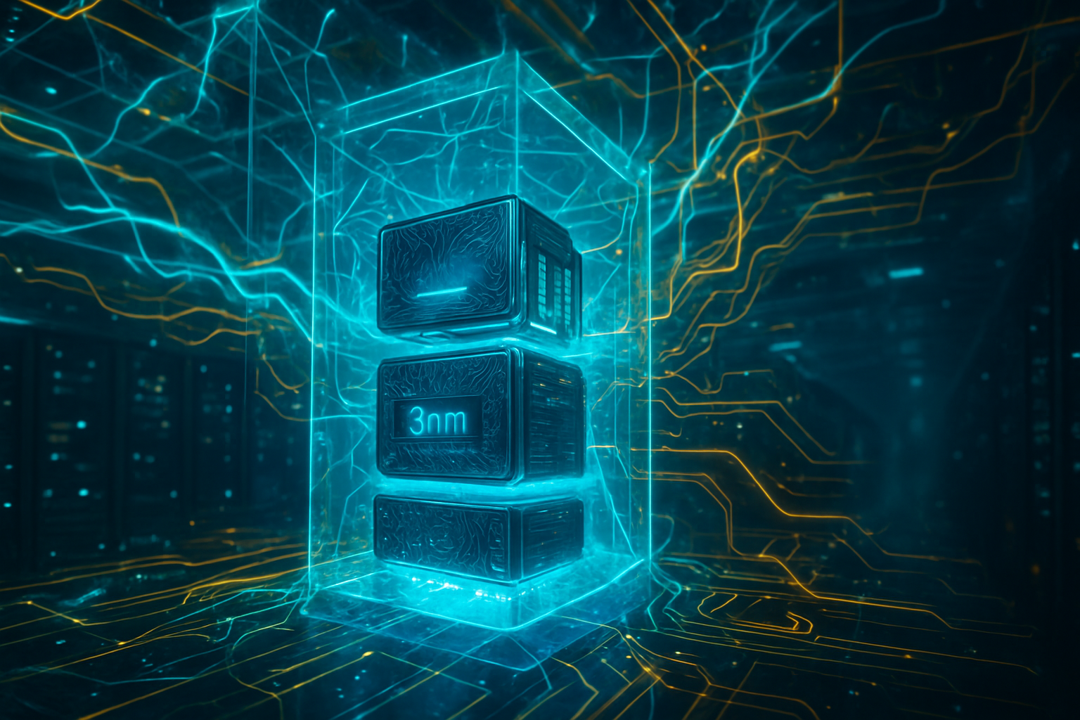
The Technical Leap: 3D-Stacked Photonics and 114 Tbps Bandwidth
At the heart of this breakthrough is Lightmatter’s Passage™ platform, a revolutionary 3D-stacked silicon photonics interconnect. Unlike previous attempts at optical networking that relied on pluggable transceivers at the edge of a board, Passage allows GPUs and other AI accelerators to be stacked directly on top of a photonic layer. The technical specifications are staggering: the Passage M1000 configuration delivers an aggregate bandwidth of 114 Terabits per second (Tbps) with a density of 1.4 Tbps/mm². This density effectively removes the "shoreline bottleneck," a long-standing constraint where data throughput was limited by the physical perimeter of the chip.
To power this massive throughput, the partnership utilizes Lightmatter’s Guide™ light engine, which leverages Very Large Scale Photonics (VLSP). This system integrates up to 64 laser wavelengths onto a single platform, eliminating the need for dozens of external laser modules and significantly reducing manufacturing complexity. GUC’s role is equally critical; as an advanced ASIC leader, they provide the sophisticated HBM3 (High Bandwidth Memory) PHY and controller designs—currently running at 8.4 Gbps—and the advanced packaging workflows necessary to bond electronic integrated circuits (EIC) with photonic integrated circuits (PIC). Using Taiwan Semiconductor Manufacturing Company (NYSE:TSM)'s CoWoS and SoIC packaging technologies, GUC ensures that these complex 3D structures can be mass-produced with high yields.
A New Competitive Landscape for the AI Giants
The transition to CPO and Silicon Photonics is creating a new hierarchy among tech giants. Companies that have traditionally dominated the networking space, such as Broadcom (NASDAQ:AVGO) and Marvell Technology (NASDAQ:MRVL), are now racing to keep pace with the integrated approach pioneered by the Lightmatter-GUC alliance. For AI chip leaders like NVIDIA (NASDAQ:NVDA) and Advanced Micro Devices (NASDAQ:AMD), the adoption of these photonic interposers is no longer optional; it is the only viable path to scaling beyond the current limits of cluster performance.
Hyperscale cloud providers—including Microsoft (NASDAQ:MSFT), Alphabet (NASDAQ:GOOGL), and Amazon (NASDAQ:AMZN)—stand to benefit most from this shift. By reducing the power consumption associated with data movement, these companies can lower the Total Cost of Ownership (TCO) for their massive AI training clusters. The partnership between Lightmatter and GUC effectively commoditizes the "optical backbone" of the chiplet era, allowing startups and smaller AI labs to design custom chips that are "photonics-ready" from day one. This level of accessibility could disrupt the current duopoly in high-end AI silicon by lowering the barrier to entry for high-bandwidth designs.
Redefining the Broader AI Landscape
The emergence of integrated optical engines is more than just a hardware upgrade; it is a fundamental shift in how we think about computing architecture. In the broader AI landscape, this milestone is being compared to the transition from vacuum tubes to transistors. For years, the "copper wall" loomed as a threat to the continued advancement of Moore’s Law and the growth of generative AI. By replacing electrons with photons for chip-to-chip communication, the industry has effectively extended the roadmap for AI scaling by another decade.
However, this transition also brings new challenges and concerns. The complexity of 3D-stacked silicon photonics introduces rigorous thermal management requirements, as lasers are notoriously sensitive to heat. Furthermore, the shift toward CPO requires a massive retooling of the semiconductor supply chain. While the $103 billion market projection for 2035 highlights the economic opportunity, it also underscores the immense capital expenditure required to transition away from copper-based standards that have been the industry's bedrock for half a century.
The Horizon: From CPO to Optical Computing
Looking ahead, the near-term focus will be the deployment of these CPO solutions in 2026-2027 within the world’s largest supercomputers. We expect to see the first "optical-first" data centers come online within the next 24 months, capable of training models with tens of trillions of parameters—orders of magnitude larger than what was possible in 2024. Experts predict that the success of the Lightmatter-GUC partnership will catalyze a wave of consolidation in the photonics space as larger players look to acquire specialized laser and modulator technologies.
In the long term, the industry is eyeing even more radical applications. Beyond just moving data, the next frontier is optical computing—using light to perform the actual mathematical calculations for AI. While currently in the early research stages, platforms like Lightmatter’s Envise are laying the groundwork for a future where the distinction between "networking" and "compute" entirely disappears. The challenge remains in perfecting the reliability of these light-based systems at scale, but the 2026 commercialization of CPO is the definitive first step.
A Comprehensive Wrap-Up
The partnership between Lightmatter and GUC represents the successful crossing of the "optical chasm." By combining cutting-edge photonic interconnects with world-class ASIC packaging, they have provided the semiconductor industry with a shovel to dig through the copper wall. The $103 billion market valuation projected by 2035 is not just a reflection of hardware sales; it is a testament to the fact that light is the only medium capable of carrying the weight of the AI revolution.
As we move further into 2026, the industry's eyes will be on the initial benchmarks of the Passage platform in real-world data center environments. This development marks a pivotal moment in AI history, ensuring that the limits of our physical materials do not dictate the limits of our artificial intelligence. For investors and tech leaders alike, the message is clear: the future of AI is moving at the speed of light.
This content is intended for informational purposes only and represents analysis of current AI developments.
TokenRing AI delivers enterprise-grade solutions for multi-agent AI workflow orchestration, AI-powered development tools, and seamless remote collaboration platforms.
For more information, visit https://www.tokenring.ai/.