In the heart of Memphis, Tennessee, a technological titan has risen with a speed that has left the traditional data center industry in a state of shock. Known as "Colossus," this massive supercomputer cluster—the brainchild of Elon Musk’s xAI—was constructed from the ground up in a mere 122 days. Built to fuel the development of the Grok large language models, the facility initially housed 100,000 NVIDIA (NASDAQ:NVDA) H100 GPUs, creating what is widely considered the most powerful AI training cluster on the planet. As of January 27, 2026, the facility has not only proven its operational viability but has already begun a massive expansion phase that targets a scale previously thought impossible.
The significance of Colossus lies not just in its raw compute power, but in the sheer logistical audacity of its creation. While typical hyperscale data centers of this magnitude often require three to four years of planning, permitting, and construction, xAI managed to achieve "power-on" status in less than four months. This rapid deployment has fundamentally rewritten the playbook for AI infrastructure, signaling a shift where speed-to-market is the ultimate competitive advantage in the race toward Artificial General Intelligence (AGI).
Engineering the Impossible: Technical Specs and the 122-Day Miracle
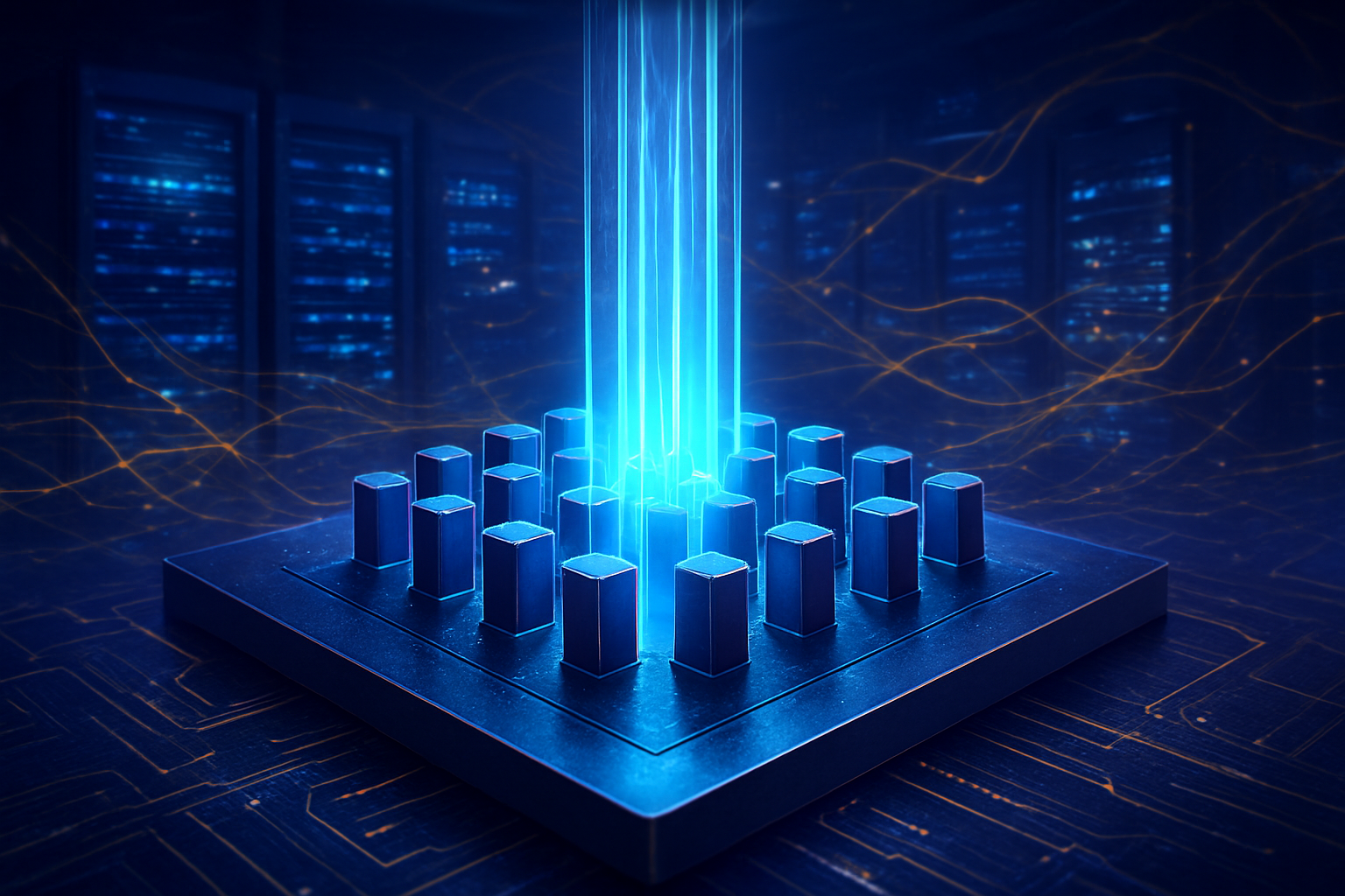
The technical foundation of Colossus is a masterclass in modern hardware orchestration. The initial deployment of 100,000 H100 GPUs was made possible through a strategic partnership with Super Micro Computer, Inc. (NASDAQ:SMCI) and Dell Technologies (NYSE:DELL), who each supplied approximately 50% of the server racks. To manage the immense heat generated by such a dense concentration of silicon, the entire system utilizes an advanced liquid-cooling architecture. Each building block consists of specialized racks housing eight 4U Universal GPU servers, which are then grouped into 512-GPU "mini-clusters" to optimize data flow and thermal management.
Beyond the raw chips, the networking fabric is what truly separates Colossus from its predecessors. The cluster utilizes NVIDIA’s Spectrum-X Ethernet platform, a networking technology specifically engineered for multi-tenant, hyperscale AI environments. While standard Ethernet often suffers from significant packet loss and throughput drops at this scale, Spectrum-X enables a staggering 95% data throughput. This is achieved through advanced congestion control and Remote Direct Memory Access (RDMA), ensuring that the GPUs spend more time calculating and less time waiting for data to travel across the network.
Initial reactions from the AI research community have ranged from awe to skepticism regarding the sustainability of such a build pace. Industry experts noted that the 19-day window between the first server rack arriving on the floor and the commencement of AI training is a feat of engineering logistics that has never been documented in the private sector. By bypassing traditional utility timelines through the use of 20 mobile natural gas turbines and a 150 MW Tesla (NASDAQ:TSLA) Megapack battery system, xAI demonstrated a "full-stack" approach to infrastructure that most competitors—reliant on third-party data center providers—simply cannot match.
Shifting the Power Balance: Competitive Implications for Big Tech
The existence of Colossus places xAI in a unique strategic position relative to established giants like OpenAI, Google, and Meta. By owning and operating its own massive-scale infrastructure, xAI avoids the "compute tax" and scheduling bottlenecks associated with public cloud providers. This vertical integration allows for faster iteration cycles for the Grok models, potentially allowing xAI to bridge the gap with its more established rivals in record time. For NVIDIA, the project serves as a premier showcase for the Hopper and now the Blackwell architectures, proving that their hardware can be deployed at a "gigawatt scale" when paired with aggressive engineering.
This development creates a high-stakes "arms race" for physical space and power. Competitors are now forced to reconsider their multi-year construction timelines, as the 122-day benchmark set by xAI has become the new metric for excellence. Major AI labs that rely on Microsoft or AWS may find themselves at a disadvantage if they cannot match the sheer density of compute available in Memphis. Furthermore, the massive $5 billion deal reported between xAI and Dell for the next generation of Blackwell-based servers underscores a shift where the supply chain itself becomes a primary theater of war.
Strategic advantages are also emerging in the realm of talent and capital. The ability to build at this speed attracts top-tier hardware and infrastructure engineers who are frustrated by the bureaucratic pace of traditional tech firms. For investors, Colossus represents a tangible asset that justifies the massive valuations of xAI, moving the company from a "software-only" play to a powerhouse that controls the entire stack—from the silicon and cooling to the weights of the neural networks themselves.
The Broader Landscape: Environmental Challenges and the New AI Milestone
Colossus fits into a broader trend of "gigafactory-scale" computing, where the focus has shifted from algorithmic efficiency to the brute force of massive hardware clusters. This milestone mirrors the historical shift in the 1940s toward massive industrial projects like the Manhattan Project, where the physical scale of the equipment was as important as the physics behind it. However, this scale comes with significant local and global impacts. The Memphis facility has faced scrutiny over its massive water consumption for cooling and its reliance on mobile gas turbines, highlighting the growing tension between rapid AI advancement and environmental sustainability.
The potential concerns regarding power consumption are not trivial. As Colossus moves toward a projected 2-gigawatt capacity by the end of 2026, the strain on local electrical grids will be immense. This has led xAI to expand into neighboring Mississippi with a new facility nicknamed "MACROHARDRR," strategically placed to leverage different power resources. This geographical expansion suggests that the future of AI will not be determined by code alone, but by which companies can successfully secure and manage the largest shares of the world's energy and water resources.
Comparisons to previous AI breakthroughs, such as the original AlphaGo or the release of GPT-3, show a marked difference in the nature of the milestone. While those were primarily mathematical and research achievements, Colossus is an achievement of industrial manufacturing and logistical coordination. It marks the era where AI training is no longer a laboratory experiment but a heavy industrial process, requiring the same level of infrastructure planning as a major automotive plant or a semiconductor fabrication facility.
Looking Ahead: Blackwell, Grok-3, and the Road to 1 Million GPUs
The future of the Memphis site and its satellite extensions is focused squarely on the next generation of silicon. xAI has already begun integrating NVIDIA's Blackwell (GB200) GPUs, which promise a 30x performance increase for LLM inference over the H100s currently in the racks. As of January 2026, tens of thousands of these new chips are reportedly coming online, with the ultimate goal of reaching a total of 1 million GPUs across all xAI sites. This expansion is expected to provide the foundation for Grok-3 and subsequent models, which Musk has hinted will surpass the current state-of-the-art in reasoning and autonomy.
Near-term developments will likely include the full transition of the Memphis grid from mobile turbines to a more permanent, high-capacity substation, coupled with an even larger deployment of Tesla Megapacks for grid stabilization. Experts predict that the next major challenge will not be the hardware itself, but the data required to keep such a massive cluster utilized. With 1 million GPUs, the "data wall"—the limit of high-quality human-generated text available for training—becomes a very real obstacle, likely pushing xAI to lean more heavily into synthetic data generation and video-based training.
The long-term applications for a cluster of this size extend far beyond chatbots. The immense compute capacity is expected to be used for complex physical simulations, the development of humanoid robot brains (Tesla's Optimus), and potentially even genomic research. As the "gigawatt scale" becomes the new standard for Tier-1 AI labs, the industry will watch closely to see if this massive investment in hardware translates into the elusive breakthrough of AGI or if it leads to a plateau in diminishing returns for LLM scaling.
A New Era of Industrial Intelligence
The story of Colossus is a testament to what can be achieved when the urgency of a startup is applied to the scale of a multi-billion dollar industrial project. In just 122 days, xAI turned a vacant facility into the world’s most concentrated hub of intelligence, fundamentally altering the expectations for AI infrastructure. The collaboration between NVIDIA, Supermicro, and Dell has proven that the global supply chain can move at "Elon time" when the stakes—and the capital—are high enough.
As we look toward the remainder of 2026, the success of Colossus will be measured by the capabilities of the models it produces. If Grok-3 achieves the leap in reasoning that its creators predict, the Memphis cluster will be remembered as the cradle of a new era of compute. Regardless of the outcome, the 122-day sprint has set a permanent benchmark, ensuring that the race for AI supremacy will be as much about concrete, copper, and cooling as it is about algorithms and data.
This content is intended for informational purposes only and represents analysis of current AI developments.
TokenRing AI delivers enterprise-grade solutions for multi-agent AI workflow orchestration, AI-powered development tools, and seamless remote collaboration platforms.
For more information, visit https://www.tokenring.ai/.