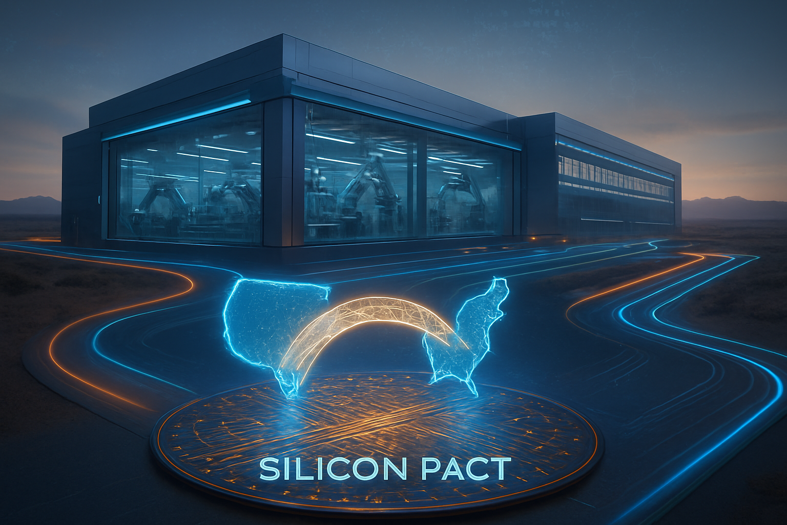
Tag: AI Infrastructure

  • The Blackwell Era: How NVIDIA’s ‘Off the Charts’ Demand is Reshaping the Global AI Landscape in 2026

    The Blackwell Era: How NVIDIA’s ‘Off the Charts’ Demand is Reshaping the Global AI Landscape in 2026

    As of January 19, 2026, the artificial intelligence sector has entered a new phase of industrial-scale deployment, driven almost entirely by the ubiquity of NVIDIA's (NASDAQ:NVDA) Blackwell architecture. What began as a highly anticipated hardware launch in late 2024 has evolved into the foundational infrastructure for the "AI Factory" era. Jensen Huang, CEO of NVIDIA, recently described the current appetite for Blackwell-based systems like the B200 and the liquid-cooled GB200 NVL72 as "off the charts," a sentiment backed by a staggering backlog of approximately 3.6 million units from major cloud service providers and sovereign nations alike.

    The significance of this moment cannot be overstated. We are no longer discussing individual chips but rather integrated, rack-scale supercomputers that function as a single unit of compute. This shift has enabled the first generation of truly "agentic" AI—models capable of multi-step reasoning and autonomous task execution—that were previously hampered by the communication bottlenecks and memory constraints of the older Hopper architecture. As Blackwell units flood into data centers across the globe, the focus of the tech industry has shifted from whether these models can be built to how quickly they can be scaled to meet a seemingly bottomless well of enterprise demand.

    The Blackwell architecture represents a radical departure from the monolithic GPU designs of the past, utilizing a dual-die chiplet approach that packs 208 billion transistors into a single package. The flagship B200 GPU delivers up to 20 PetaFLOPS of FP4 performance, a five-fold increase over the H100’s peak throughput. Central to this leap is the second-generation Transformer Engine, which introduces support for 4-bit floating point (FP4) precision. This allows massive Large Language Models (LLMs) to run with twice the throughput and significantly lower memory footprints without sacrificing accuracy, effectively doubling the "intelligence per watt" compared to previous generations.

    Beyond the raw compute power, the real breakthrough of 2026 is the GB200 NVL72 system. By interconnecting 72 Blackwell GPUs with the fifth-generation NVLink (offering 1.8 TB/s of bidirectional bandwidth), NVIDIA has created a single entity capable of 1.4 ExaFLOPS of AI inference. This "rack-as-a-GPU" philosophy addresses the massive communication overhead inherent in Mixture-of-Experts (MoE) models, where data must be routed between specialized "expert" layers across multiple chips at microsecond speeds. Initial reactions from the research community suggest that Blackwell has reduced the cost of training frontier models by over 60%, while the dedicated hardware decompression engine has accelerated data loading by up to 800 GB/s, removing one of the last major bottlenecks in deep learning pipelines.

    The deployment of Blackwell has solidified a "winner-takes-most" dynamic among hyperscalers. Microsoft (NASDAQ:MSFT) has emerged as a primary beneficiary, integrating Blackwell into its "Fairwater" AI superfactories to power the Azure OpenAI Service. These clusters are reportedly processing over 100 trillion tokens per quarter, supporting a new wave of enterprise-grade AI agents. Similarly, Amazon (NASDAQ:AMZN) Web Services has leveraged a multi-billion dollar agreement to deploy Blackwell and the upcoming Rubin chips within its EKS environment, facilitating "gigascale" generative AI for its global customer base. Alphabet (NASDAQ:GOOGL), while continuing to develop its internal TPU silicon, remains a major Blackwell customer to ensure its Google Cloud Platform remains a competitive destination for multi-cloud AI workloads.

    However, the competitive landscape is far from static. Advanced Micro Devices (NASDAQ:AMD) has countered with its Instinct MI400 series, which features a massive 432GB of HBM4 memory. By emphasizing "Open Standards" through UALink and Ultra Ethernet, AMD is positioning itself as the primary alternative for organizations wary of NVIDIA’s proprietary ecosystem. Meanwhile, Intel (NASDAQ:INTC) has pivoted its strategy toward the "Jaguar Shores" platform, focusing on the cost-effective "sovereign AI" market. Despite these efforts, NVIDIA’s deep software moat—specifically the CUDA 13.0 stack—continues to make Blackwell the default choice for developers, creating a strategic advantage that rivals are struggling to erode as the industry standardizes on Blackwell-native architectures.

    The broader significance of the Blackwell rollout extends into the realms of energy policy and national security. The power density of these new clusters is unprecedented; a single GB200 NVL72 rack can draw up to 120kW, requiring advanced liquid cooling infrastructure that many older data centers simply cannot support. This has triggered a global "cooling gold rush" and pushed data center electricity demand toward an estimated 1,000 TWh annually. Paradoxically, the 25x increase in energy efficiency for inference has allowed for the "Inference Supercycle," where the cost of running a sophisticated AI model has plummeted to a fraction of a cent per thousand tokens, making high-level reasoning accessible to small businesses and individual developers.

    Furthermore, we are witnessing the rise of "Sovereign AI." Nations now view compute capacity as a critical national resource. In Europe, countries like France and the UK have launched multi-billion dollar infrastructure programs—such as "Stargate UK"—to build domestic Blackwell clusters. In Asia, Saudi Arabia’s "Project HUMAIN" is constructing massive 6-gigawatt AI data centers, while India’s National AI Compute Grid is deploying over 10,000 GPUs to support regional language models. This trend suggests a future where AI capability is as geopolitically significant as oil reserves or semiconductor manufacturing capacity, with Blackwell serving as the primary currency of this new digital economy.

    Looking ahead to the remainder of 2026 and into 2027, the focus is already shifting toward NVIDIA’s next milestone: the Rubin (R100) architecture. Expected to enter mass availability in the second half of 2026, Rubin will mark the definitive transition to HBM4 memory and a 3nm process node, promising a further 3.5x improvement in training performance. We expect to see the "Blackwell Ultra" (B300) serve as a bridge, offering 288GB of HBM3e memory to support the increasingly massive context windows required by video-generative models and autonomous coding agents.

    The next frontier for these systems will be "Physical AI"—the integration of Blackwell-scale compute into robotics and autonomous manufacturing. With the computational overhead of real-time world modeling finally becoming manageable, we anticipate the first widespread deployment of humanoid robots powered by "miniaturized" Blackwell architectures by late 2027. The primary challenge remains the global supply chain for High Bandwidth Memory (HBM), where manufacturers like SK Hynix (KRX:000660) and TSMC (NYSE:TSM) are operating at maximum capacity to meet NVIDIA's relentless release cycle.

    In summary, the early 2026 landscape is defined by the transition of AI from a specialized experimental tool to a core utility of the global economy, powered by NVIDIA’s Blackwell architecture. The "off the charts" demand described by Jensen Huang is not merely hype; it is a reflection of a fundemental shift in how computing is performed, moving away from general-purpose CPUs toward accelerated, interconnected AI factories.

    As we move forward, the key metrics to watch will be the stabilization of energy-efficient cooling solutions and the progress of the Rubin architecture. Blackwell has set a high bar, effectively ending the era of "dumb" chatbots and ushering in an age of reasoning agents. Its legacy will be recorded as the moment when the "intelligence per watt" curve finally aligned with the needs of global industry, making the promise of ubiquitous artificial intelligence a physical and economic reality.


    This content is intended for informational purposes only and represents analysis of current AI developments.

    TokenRing AI delivers enterprise-grade solutions for multi-agent AI workflow orchestration, AI-powered development tools, and seamless remote collaboration platforms.
    For more information, visit https://www.tokenring.ai/.

  • China’s “Sovereign” Silicon: Breakthrough in Domestic High-Energy Ion Implantation

    China’s “Sovereign” Silicon: Breakthrough in Domestic High-Energy Ion Implantation

    In a milestone that signals a definitive shift in the global semiconductor balance of power, the China Institute of Atomic Energy (CIAE) announced on January 12, 2026, the successful beam extraction and performance validation of the POWER-750H, China’s first domestically developed tandem-type high-energy hydrogen ion implanter. This development represents the completion of the "final piece" in China’s domestic chipmaking puzzle, closing the technology gap in one of the few remaining "bottleneck" areas where the country was previously 100% dependent on imports from US and Japanese vendors.

    The immediate significance of the POWER-750H cannot be overstated. High-energy ion implantation is a critical process for manufacturing the specialized power semiconductors and image sensors that drive modern AI data centers and electric vehicles. By mastering this technology amidst intensifying trade restrictions, China has effectively neutralized a key lever of Western export controls, securing the foundational equipment needed to scale its internal AI infrastructure and power electronics industry without fear of further technological decapitation.

    Technical Mastery: The Power of Tandem Acceleration

    The POWER-750H is not merely an incremental improvement but a fundamental leap in domestic precision engineering. Unlike standard medium-current implanters, high-energy systems must accelerate ions to mega-electron volt (MeV) levels to penetrate deep into silicon wafers. The "750" in its designation refers to its 750kV high-voltage terminal, which, through tandem acceleration, allows it to generate ion beams with effective energies exceeding 1.5 MeV. This technical capability is essential for "deep junction" doping—a process required to create the robust transistors found in high-voltage power management ICs (PMICs) and high-density memory.

    Technically, the POWER-750H differs from previous Chinese attempts by utilizing a tandem accelerator architecture, which uses a single high-voltage terminal to accelerate ions twice, significantly increasing energy efficiency and beam stability within a smaller footprint. This approach mirrors the advanced systems produced by industry leaders like Axcelis Technologies (NASDAQ: ACLS), yet it has been optimized for the specific "profile engineering" required for wide-bandgap semiconductors like Silicon Carbide (SiC) and Gallium Nitride (GaN). Initial reactions from the domestic research community suggest that the POWER-750H achieves a beam purity and dose uniformity that rivals the venerable Purion series from Axcelis, marking a transition from laboratory prototype to industrial-grade tool.

    Market Seismic Shifts: SMIC, Wanye, and the Retreat of the Giants

    The commercialization of these tools is already reshaping the financial landscape of the semiconductor industry. SMIC (HKG: 0981), China’s largest foundry, has reportedly recalibrated its 2026 capital expenditure (CAPEX) strategy, allocating over 70% of its equipment budget to domestic vendors. This "national team" pivot has provided a massive tailwind for Wanye Enterprises (SHA: 600641), whose subsidiary, Kingsemi, has moved into mass deployment of high-energy models. Market analysts predict that Wanye will capture nearly 40% of the domestic ion implanter market share by the end of 2026, a space that was once an uncontested monopoly for Western firms.

    Conversely, the impact on US equipment giants has been severe. Applied Materials (NASDAQ: AMAT), which historically derived a significant portion of its revenue from the Chinese market, has seen its China-based sales guidance drop from 40% to approximately 25% for the 2026 fiscal year. Even more dramatic was the late-2025 defensive merger between Axcelis and Veeco Instruments (NASDAQ: VECO), a move widely interpreted as an attempt to diversify away from a pure-play ion implantation focus as Chinese domestic alternatives began to saturate the power semiconductor market. The loss of the Chinese "legacy node" and power-chip markets has forced these companies to pivot aggressively toward advanced packaging and High Bandwidth Memory (HBM) tools in the US and South Korea to sustain growth.

    The AI Connection: Powering the Factories of the Future

    Beyond the fabrication of logic chips, the significance of high-energy ion implantation lies in its role in the "AI infrastructure supercycle." Modern AI data centers, which are projected to consume massive amounts of power by the end of 2026, rely on high-efficiency power management systems to operate. Domestic high-energy implanters allow China to produce the specialized MOSFETs and IGBTs needed for these data centers internally. This ensures that China's push for "AI Sovereignty"—the ability to train and run massive large language models on an entirely domestic hardware stack—remains on track.

    This milestone is a pivotal moment in the broader trend of global "de-globalization" in tech. Just as the US has sought to restrict China’s access to 3nm and 5nm lithography, China has responded by achieving self-sufficiency in the tools required for the "power backbone" of AI. This mirrors previous breakthroughs in etching and thin-film deposition, signaling that the era of using semiconductor equipment as a geopolitical weapon may be reaching a point of diminishing returns. The primary concern among international observers is that a fully decoupled supply chain could lead to a divergence in technical standards, potentially slowing the global pace of AI innovation through fragmentation.

    The Horizon: From 28nm to the Sub-7nm Frontier

    Looking ahead, the near-term focus for Chinese equipment manufacturers is the qualification of high-energy tools for the 14nm and 7nm nodes. While the POWER-750H is currently optimized for power chips and 28nm logic, engineers at CETC and Kingsemi are already working on "ultra-high-energy" variants capable of the 5 MeV+ levels required for advanced CMOS image sensors and 3D NAND flash memory. These future iterations are expected to incorporate more advanced automation and AI-driven process control to further increase wafer throughput.

    The most anticipated development on the horizon is the integration of these domestic tools into the production lines for Huawei’s next-generation Ascend 910D AI accelerators. Experts predict that by late 2026, China will demonstrate a "fully domestic" 7nm production line that utilizes zero US-origin equipment. The challenge remains in achieving the extreme ultraviolet (EUV) lithography parity required for sub-5nm chips, but with the ion implantation hurdle cleared, the path toward total semiconductor independence is more visible than ever.

    A New Era of Semiconductor Sovereignty

    The announcement of the POWER-750H is more than a technical victory; it is a geopolitical statement. It marks the moment when China transitioned from being a consumer of semiconductor technology to a self-sustaining architect of its own silicon future. The key takeaway for the tech industry is that the window for using specialized equipment exports to stifle Chinese semiconductor growth is rapidly closing.

    In the coming months, the industry will be watching for the first production data from SMIC’s domestic-only lines and the potential for these Chinese tools to begin appearing in secondary markets in Southeast Asia and Europe. As 2026 unfolds, the successful deployment of the POWER-750H will likely be remembered as the event that solidified the "Two-Track" global semiconductor ecosystem, forever changing the competitive dynamics of the AI and chipmaking industries.


    This content is intended for informational purposes only and represents analysis of current AI and semiconductor developments.

    TokenRing AI delivers enterprise-grade solutions for multi-agent AI workflow orchestration, AI-powered development tools, and seamless remote collaboration platforms.
    For more information, visit https://www.tokenring.ai/.

  • Intel’s 18A Sovereignty: The Silicon Giant Reclaims the Process Lead in the AI Era

    Intel’s 18A Sovereignty: The Silicon Giant Reclaims the Process Lead in the AI Era

    As of January 19, 2026, the global semiconductor landscape has undergone a tectonic shift. After nearly a decade of playing catch-up to Asian rivals, Intel (NASDAQ: INTC) has officially entered high-volume manufacturing (HVM) for its 18A (1.8nm-class) process node. This milestone marks the successful completion of CEO Pat Gelsinger’s audacious "five nodes in four years" roadmap, a feat many industry skeptics deemed impossible when it was first announced. The 18A node is not merely a technical incremental step; it is the cornerstone of Intel’s "IDM 2.0" strategy, designed to transform the company into a world-class foundry that rivals TSMC (NYSE: TSM) while simultaneously powering its own next-generation AI silicon.

    The immediate significance of 18A lies in its marriage of two revolutionary technologies: RibbonFET and PowerVia. By being the first to bring backside power delivery and gate-all-around (GAA) transistors to the mass market at this scale, Intel has effectively leapfrogged its competitors in performance-per-watt efficiency. With the first "Panther Lake" consumer chips hitting shelves next week and "Clearwater Forest" Xeon processors already shipping to hyperscale data centers, 18A has moved from a laboratory ambition to the primary engine of the AI hardware revolution.

    The Architecture of Dominance: RibbonFET and PowerVia

    Technically, 18A represents the most significant architectural overhaul in semiconductor manufacturing since the introduction of FinFET over a decade ago. At the heart of the node is RibbonFET, Intel's implementation of Gate-All-Around (GAA) transistor technology. Unlike the previous FinFET design, where the gate contacted the channel on three sides, RibbonFET stacks multiple nanoribbons vertically, with the gate wrapping entirely around the channel. This configuration provides superior electrostatic control, drastically reducing current leakage and allowing transistors to switch faster at significantly lower voltages. Industry experts note that this level of control is essential for the high-frequency demands of modern AI training and inference.

    Complementing RibbonFET is PowerVia, Intel’s proprietary version of backside power delivery. Historically, both power and data signals competed for space on the front of the silicon wafer, leading to a "congested" wiring environment that caused electrical interference and voltage droop. PowerVia moves the entire power delivery network to the back of the wafer, decoupling it from the signal routing on the top. This innovation allows for up to a 30% increase in transistor density and a significant boost in power efficiency. While TSMC (NYSE: TSM) has opted to wait until its A16 node to implement similar backside power tech, Intel’s "first-mover" advantage with PowerVia has given it a roughly 18-month lead in this specific power-delivery architecture.

    Initial reactions from the semiconductor research community have been overwhelmingly positive. TechInsights and other industry analysts have reported that 18A yields have crossed the 65% threshold—a critical "gold standard" for commercial viability. Experts suggest that by separating power and signal, Intel has solved one of the most persistent bottlenecks in chip design: the "RC delay" that occurs when signals travel through thin, high-resistance wires. This technical breakthrough has allowed Intel to reclaim the title of the world’s most advanced logic manufacturer, at least for the current 2026 cycle.

    A New Customer Portfolio: Microsoft, Amazon, and the Apple Pivot

    The success of 18A has fundamentally altered the competitive dynamics of the foundry market. Intel Foundry has successfully secured several "whale" customers who were previously exclusive to TSMC. Most notably, Microsoft (NASDAQ: MSFT) has confirmed that its next generation of custom Maia AI accelerators is being manufactured on the 18A node. Similarly, Amazon (NASDAQ: AMZN) has partnered with Intel to produce custom AI fabric silicon for its AWS Graviton and Trainium 3 platforms. These wins demonstrate that the world’s largest cloud providers are no longer willing to rely on a single source for their most critical AI infrastructure.

    Perhaps the most shocking development of late 2025 was the revelation that Apple (NASDAQ: AAPL) had qualified Intel 18A for a portion of its M-series silicon production. While TSMC remains Apple’s primary partner, the move to Intel for entry-level MacBook and iPad chips marks the first time in a decade that Apple has diversified its cutting-edge logic manufacturing. For Intel, this is a massive validation of the IDM 2.0 model, proving that its foundry services can meet the exacting standards of the world’s most demanding hardware company.

    This shift puts immense pressure on NVIDIA (NASDAQ: NVDA) and Advanced Micro Devices (NASDAQ: AMD). While NVIDIA has traditionally been conservative with its foundry choices, the superior performance-per-watt of 18A—specifically for high-density AI clusters—has led to persistent rumors that NVIDIA’s "Rubin" successor might utilize a multi-foundry approach involving Intel. The strategic advantage for these companies lies in supply chain resilience; by utilizing Intel’s domestic Fabs in Arizona and Ohio, they can mitigate the geopolitical risks associated with manufacturing exclusively in the Taiwan Strait.

    Geopolitics and the AI Power Struggle

    The broader significance of Intel’s 18A achievement cannot be overstated. It represents a pivot point for Western semiconductor sovereignty. As AI becomes the defining technology of the decade, the ability to manufacture the underlying chips domestically is now a matter of national security. Intel’s progress is a clear win for the U.S. CHIPS Act, as much of the 18A capacity is housed in the newly operational Fab 52 in Arizona. This domestic "leading-edge" capability provides a cushion against global supply chain shocks that have plagued the industry in years past.

    In the context of the AI landscape, 18A arrives at a time when the "power wall" has become the primary limit on AI model growth. As LLMs (Large Language Models) grow in complexity, the energy required to train and run them has skyrocketed. The efficiency gains provided by PowerVia and RibbonFET are precisely what hyperscalers like Meta (NASDAQ: META) and Alphabet (NASDAQ: GOOGL) need to keep their AI ambitions sustainable. By reducing the energy footprint of each transistor switch, Intel 18A is effectively enabling the next order of magnitude in AI compute scaling.

    However, challenges remain. While Intel leads in backside power, TSMC’s N2 node still maintains a slight advantage in absolute SRAM density—the memory used for on-chip caches that are vital for AI performance. The industry is watching closely to see if Intel can maintain its execution momentum as it transitions from 18A to the even more ambitious 14A node. The comparison to the "14nm era," where Intel remained stuck on a single node for years, is frequently cited by skeptics as a cautionary tale.

    The Road to 14A and High-NA EUV

    Looking ahead, the 18A node is just the beginning of Intel’s long-term roadmap. The company has already begun "risk production" for its 14A node, which will be the first in the world to utilize High-NA (Numerical Aperture) EUV lithography from ASML (NASDAQ: ASML). This next-generation machinery allows for even finer features to be printed on silicon, potentially pushing transistor counts into the hundreds of billions on a single die. Experts predict that 14A will be the node that truly determines if Intel can hold its lead through the end of the decade.

    In the near term, we can expect a flurry of 18A-based product announcements throughout 2026. Beyond CPUs and AI accelerators, the 18A node is expected to be a popular choice for automotive silicon and high-performance networking chips, where the combination of high speed and low heat is critical. The primary challenge for Intel now is "scaling the ecosystem"—ensuring that the design tools (EDA) and IP blocks from partners like Synopsys (NASDAQ: SNPS) and Cadence (NASDAQ: CDNS) are fully optimized for the unique power-delivery characteristics of 18A.

    Final Verdict: A New Chapter for Silicon Valley

    The successful rollout of Intel 18A is a watershed moment in the history of computing. It signifies the end of Intel’s "stagnation" era and the birth of a viable, Western-led alternative to the TSMC monopoly. For the AI industry, 18A provides the necessary hardware foundation to continue the current pace of innovation, offering a path to higher performance without a proportional increase in energy consumption.

    In the coming weeks and months, the focus will shift from "can they build it?" to "how much can they build?" Yield consistency and the speed of the Arizona Fab ramp-up will be the key metrics for investors and customers alike. While TSMC is already preparing its A16 response, for the first time in many years, Intel is not the one playing catch-up—it is the one setting the pace.


    This content is intended for informational purposes only and represents analysis of current AI developments.

    TokenRing AI delivers enterprise-grade solutions for multi-agent AI workflow orchestration, AI-powered development tools, and seamless remote collaboration platforms.
    For more information, visit https://www.tokenring.ai/.

  • Chasing the Trillion-Dollar Frontier: AI and Next-Gen Auto Drive Chip Market to Historic Heights

    Chasing the Trillion-Dollar Frontier: AI and Next-Gen Auto Drive Chip Market to Historic Heights

    As of January 19, 2026, the global semiconductor industry stands on the precipice of a historic milestone. Once a cyclical sector defined by the ebbs and flows of consumer electronics, the chip market has transformed into a secular powerhouse. Recent projections from BofA Securities and leading consulting firms like McKinsey & Company indicate that the global chip market is no longer merely "on track" to reach $1 trillion by 2030—it is likely to cross that threshold as early as late 2026 or 2027. This acceleration, driven by an insatiable demand for Generative AI infrastructure and a fundamental architecture shift in the automotive and industrial sectors, marks the beginning of what many are calling the "Semiconductor Decade."

    The immediate significance of this growth cannot be overstated. In 2023, the industry generated roughly $527 billion in revenue. By the end of 2025, that figure had surged to approximately $793 billion. This meteoric rise is underpinned by the transition from general-purpose computing to "accelerated computing," where specialized silicon is required to handle the massive datasets of the AI era. As the world moves toward sovereign AI clouds and autonomous physical systems, the semiconductor has solidified its status as the "new oil," a critical resource for national security and economic dominance.

    The Technical Vanguard: Rubin, HBM4, and the 2nm Leap

    The push toward the $1 trillion mark is being fueled by a series of unprecedented technical breakthroughs. At the forefront is the launch of the Nvidia (NASDAQ: NVDA) Rubin platform, which officially succeeded the Blackwell architecture at the start of 2026. The Rubin R100 GPU represents a paradigm shift, delivering an estimated 50 Petaflops of FP4 compute performance. This is achieved through the first-ever exclusive use of High Bandwidth Memory 4 (HBM4). Unlike its predecessors, HBM4 doubles the interface width to 2048-bit, effectively shattering the "memory wall" that has long throttled AI training speeds.

    Manufacturing has also entered the "Angstrom Era." TSMC (NYSE: TSM) has successfully reached high-volume manufacturing for its 2nm (N2) node, utilizing Nanosheet Gate-All-Around (GAA) transistors for the first time. Simultaneously, Intel (NASDAQ: INTC) has reported stable yields for its 18A (1.8nm) process, marking a successful deployment of RibbonFET and PowerVia backside power delivery. These technologies allow for higher transistor density and significantly improved energy efficiency—a prerequisite for the next generation of data centers that are already straining global power grids.

    Furthermore, the "Power Revolution" in automotive and industrial IoT is being led by Wide-Bandgap (WBG) materials. Silicon Carbide (SiC) has transitioned to 200mm (8-inch) wafers, enabling 800V architectures to become the standard for electric vehicles (EVs). These chips provide a 7% range improvement over traditional silicon, a critical factor for the mass adoption of EVs. In the industrial space, Infineon (OTC: IFNNY) has pioneered 300mm Gallium Nitride (GaN) production, which has unlocked 30% efficiency gains for AI-driven smart factories and renewable energy grids.

    Market Dominance and the Battle for Silicon Supremacy

    The shift toward a $1 trillion market is reshuffling the corporate leaderboard. Nvidia has solidified its position as the world’s largest semiconductor company by revenue, surpassing legacy giants Samsung (KRX: 005930) and Intel. However, the ecosystem’s growth is benefiting a broad spectrum of players. Broadcom (NASDAQ: AVGO) has seen its networking and custom ASIC business skyrocket as hyperscalers like Meta and Google seek to build proprietary AI accelerators to reduce their reliance on off-the-shelf components.

    The competitive landscape is also being defined by the "Foundry War" between TSMC, Intel, and Samsung. TSMC remains the dominant player, securing nearly all of the world’s 2nm capacity for 2026, while Intel’s 18A node has successfully attracted high-profile foundry customers like Microsoft (NASDAQ: MSFT) and Amazon (NASDAQ: AMZN). This diversification of the manufacturing base is seen as a strategic advantage for the U.S. and Europe, which have leveraged the CHIPS Act to incentivize domestic production and insulate the supply chain from geopolitical volatility.

    Startups and mid-sized firms are also finding niches in the "Edge AI" and RISC-V sectors. As companies like Qualcomm (NASDAQ: QCOM) and AMD (NASDAQ: AMD) push AI capabilities directly into smartphones and PCs, the demand for low-power, highly customized silicon has surged. RISC-V, an open-standard instruction set architecture, has reached a 25% market share in specialized segments, allowing manufacturers to bypass expensive licensing fees and design chips tailored for specific AI agentic workflows.

    Geopolitics, Sovereignty, and the AI Landscape

    The broader significance of the trillion-dollar chip market lies in its intersection with global politics and sustainability. We have entered the era of "Sovereign AI," where nations are treating semiconductor capacity as a pillar of national identity. Countries across the Middle East, Europe, and Asia are investing billions to build localized data centers and domestic chip design capabilities. This trend is a departure from the globalized efficiency of the 2010s, favoring resiliency and self-reliance over lowest-cost production.

    However, this rapid expansion has raised significant concerns regarding environmental impact. The energy consumption of AI data centers is projected to double by 2030. This has placed immense pressure on chipmakers to innovate in "green silicon"—chips that provide more compute-per-watt. The transition to GaN and SiC is part of this solution, but experts warn that the sheer scale of the $1 trillion market will require even more radical breakthroughs in photonic computing and 3D chip stacking to keep emissions in check.

    Comparatively, the current AI milestone exceeds the "Internet Boom" of the late 90s in both scale and speed. While the internet era was defined by connectivity, the AI era is defined by autonomy. The chips being produced in 2026 are not just processors; they are the "brains" for autonomous robots, software-defined vehicles, and real-time industrial optimizers. This shift from passive tools to active agents marks a fundamental change in how technology integrates with human society.

    Looking Ahead: The 1.4nm Frontier and Humanoid Robotics

    As we look toward the 2027–2030 window, the roadmap is already being drawn. The next great challenge will be the move to 1.4nm (A14) nodes, which will require the full-scale deployment of High-NA EUV lithography machines from ASML (NASDAQ: ASML). These machines, costing over $350 million each, are the only way to print the intricate features required for the "Feynman" architecture—Nvidia’s projected successor to Rubin, which aims to cross the 100 Petaflop threshold.

    The near-term applications will increasingly focus on "Physical AI." While 2024 and 2025 were the years of the LLM (Large Language Model), 2026 and 2027 are expected to be the years of the LBM (Large Behavior Model). This will drive a massive surge in demand for specialized "robotic" chips—processors that combine high-speed AI inference with low-latency sensor fusion to power humanoid assistants and autonomous delivery fleets. Addressing the thermal and power constraints of these mobile units will be the primary hurdle for engineers over the next 24 months.

    A Trillion-Dollar Legacy

    The semiconductor industry's journey to $1 trillion represents one of the greatest industrial expansions in history. What was once a niche component in specialized machinery has become the heartbeat of the global economy. The key takeaway from the current market data is that the "AI super-cycle" is not a temporary bubble, but a foundational shift in the structure of technology.

    In the coming weeks and months, investors and industry watchers should keep a close eye on the rollout of HBM4 samples and the first production runs of Intel 18A. These developments will be the ultimate litmus test for whether the industry can maintain its current breakneck pace. As we cross the $1 trillion threshold, the focus will likely shift from building capacity to optimizing efficiency, ensuring that the AI revolution is as sustainable as it is transformative.


    This content is intended for informational purposes only and represents analysis of current AI developments.

    TokenRing AI delivers enterprise-grade solutions for multi-agent AI workflow orchestration, AI-powered development tools, and seamless remote collaboration platforms.
    For more information, visit https://www.tokenring.ai/.

  • Meta’s 6.6-Gigawatt Nuclear “Super-Deal” to Power the Dawn of Artificial Superintelligence

    Meta’s 6.6-Gigawatt Nuclear “Super-Deal” to Power the Dawn of Artificial Superintelligence

    In a move that fundamentally reshapes the relationship between Big Tech and the global energy grid, Meta Platforms, Inc. (NASDAQ: META) has announced a staggering 6.6-gigawatt (GW) nuclear energy portfolio to fuel its next generation of AI infrastructure. On January 9, 2026, the social media and AI titan unveiled a series of landmark agreements with Vistra Corp (NYSE: VST), Oklo Inc (NYSE: OKLO), and the Bill Gates-founded TerraPower. These multi-decade partnerships represent the single largest private procurement of nuclear power in history, marking a decisive shift toward permanent, carbon-free baseload energy for the massive compute clusters required to achieve artificial general intelligence (AGI).

    The announcement solidifies Meta’s transition from a software-centric company to a vertically integrated compute-and-power powerhouse. By securing nearly seven gigawatts of dedicated nuclear capacity, Meta is addressing the "energy wall" that has threatened to stall AI scaling. The deal specifically targets the development of "Gigawatt-scale" data center clusters—industrial-scale supercomputers that consume as much power as a mid-sized American city. This strategic pivot ensures that as Meta’s AI models grow in complexity, the physical infrastructure supporting them will remain resilient, sustainable, and independent of the fluctuating prices of the traditional energy market.

    The Architecture of Atomic Intelligence: SMRs and Legacy Uprates

    Meta’s nuclear strategy is a sophisticated three-pronged approach that blends the modernization of existing infrastructure with the pioneering of next-generation reactor technology. The cornerstone of the immediate energy supply comes from Vistra Corp, with Meta signing 20-year Power Purchase Agreements (PPAs) to source over 2.1 GW from the Perry, Davis-Besse, and Beaver Valley nuclear plants. Beyond simple procurement, Meta is funding "uprates"—technical modifications to existing reactors that increase their efficiency and output—adding an additional 433 MW of new, carbon-free capacity to the PJM grid. This "brownfield" strategy allows Meta to bring new power online faster than building from scratch.

    For its long-term needs, Meta is betting heavily on Small Modular Reactors (SMRs). The partnership with Oklo Inc involves the development of a 1.2 GW "nuclear campus" in Pike County, Ohio. Utilizing Oklo’s Aurora Powerhouse technology, this campus will feature a fleet of fast fission reactors that can operate on both fresh and recycled nuclear fuel. Unlike traditional massive light-water reactors, these SMRs are designed for rapid deployment and can be co-located with data centers to minimize transmission losses. Meta has opted for a "Power as a Service" model with Oklo, providing upfront capital to de-risk the development phase and ensure a dedicated pipeline of energy through the 2030s.

    The most technically advanced component of the deal is the partnership with TerraPower for its Natrium reactor technology. These units utilize a sodium-cooled fast reactor combined with a molten salt energy storage system. This unique design allows the reactors to provide a steady 345 MW of baseload power while possessing the ability to "flex" up to 500 MW for over five hours to meet the high-demand spikes inherent in AI training runs. Meta has secured rights to two initial units with options for six more, totaling a potential 2.8 GW. This flexibility is a radical departure from the "always-on" nature of traditional nuclear, providing a dynamic energy source that matches the variable workloads of modern AI.

    The Trillion-Dollar Power Play: Market and Competitive Implications

    This massive energy grab places Meta at the forefront of the "Compute-Energy Nexus," a term now widely used by industry analysts to describe the merging of the tech and utility sectors. While Microsoft Corp (NASDAQ: MSFT) and Amazon.com, Inc. (NASDAQ: AMZN) made early waves in 2024 and 2025 with their respective deals for the Three Mile Island and Talen Energy sites, Meta’s 6.6 GW portfolio is significantly larger in both scope and technological diversity. By locking in long-term, fixed-price energy contracts, Meta is insulating itself from the energy volatility that its competitors may face as the global grid struggles to keep up with AI-driven demand.

    The primary beneficiaries of this deal are the nuclear innovators themselves. Following the announcement, shares of Vistra Corp and Oklo Inc saw significant surges, with Oklo being viewed as the "Apple of Energy"—a design-led firm with a massive, guaranteed customer in Meta. For TerraPower, the deal provides the commercial validation and capital injection needed to move Natrium from the pilot stage to industrial-scale deployment. This creates a powerful signal to the market: nuclear is no longer a "last resort" for green energy, but the primary engine for the next industrial revolution.

    However, this aggressive procurement has also raised concerns among smaller AI startups and research labs. As tech giants like Meta, Google—owned by Alphabet Inc (NASDAQ: GOOGL)—and Microsoft consolidate the world's available carbon-free energy, the "energy barrier to entry" for new AI companies becomes nearly insurmountable. The strategic advantage here is clear: those who control the power, control the compute. Meta's ability to build "Gigawatt" clusters like the 1 GW Prometheus in Ohio and the planned 5 GW Hyperion in Louisiana effectively creates a "moat of electricity" that could marginalize any competitor without its own dedicated power source.

    Beyond the Grid: AI’s Environmental and Societal Nuclear Renaissance

    The broader significance of Meta's nuclear pivot cannot be overstated. It marks a historic reconciliation between the environmental goals of the tech industry and the high energy demands of AI. For years, critics argued that the "AI boom" would lead to a resurgence in coal and natural gas; instead, Meta is using AI as the primary catalyst for a nuclear renaissance. By funding the "uprating" of old plants and the construction of new SMRs, Meta is effectively modernizing the American energy grid, providing a massive influx of private capital into a sector that has been largely stagnant for three decades.

    This development also reflects a fundamental shift in the AI landscape. We are moving away from the era of "efficiency-first" AI and into the era of "brute-force scaling." The "Gigawatt" data center is a testament to the belief that the path to AGI requires an almost unfathomable amount of physical resources. Comparing this to previous milestones, such as the 2012 AlexNet breakthrough or the 2022 launch of ChatGPT, the current milestone is not a change in code, but a change in matter. We are now measuring AI progress in terms of hectares of land, tons of cooling water, and gigawatts of nuclear energy.

    Despite the optimism, the move has sparked intense debate over grid equity and safety. While Meta is funding new capacity, the sheer volume of power it requires could still strain regional grids, potentially driving up costs for residential consumers in the PJM and MISO regions. Furthermore, the reliance on SMRs—a technology that is still in its commercial infancy—carries inherent regulatory and construction risks. The industry is watching closely to see if the Nuclear Regulatory Commission (NRC) can keep pace with the "Silicon Valley speed" that Meta and its partners are demanding.

    The Road to Hyperion: What’s Next for Meta’s Infrastructure

    In the near term, the focus will shift from contracts to construction. The first major milestone is the 1 GW Prometheus cluster in New Albany, Ohio, expected to go fully operational by late 2026. This facility will serve as the "blueprint" for future sites, integrating the energy from Vistra's nuclear uprates directly into the high-voltage fabric of Meta's most advanced AI training facility. Success here will determine the feasibility of the even more ambitious Hyperion project in Louisiana, which aims to reach 5 GW by the end of the decade.

    The long-term challenge remains the delivery of the SMR fleet. Oklo and TerraPower must navigate a complex landscape of supply chain hurdles, specialized labor shortages, and stringent safety testing. If successful, the applications for this "boundless" compute are transformative. Experts predict that Meta will use this power to run "infinite-context" models and real-time physical world simulations that could accelerate breakthroughs in materials science, drug discovery, and climate modeling—ironically using the very AI that consumes the energy to find more efficient ways to produce and save it.

    Conclusion: A New Era of Atomic-Scale Computing

    Meta’s 6.6 GW nuclear commitment is more than just a series of power deals; it is a declaration of intent for the age of Artificial Superintelligence. By partnering with Vistra, Oklo, and TerraPower, Meta has secured the physical foundation necessary to sustain its vision of the future. The significance of this development in AI history lies in its scale—it is the moment when the digital world fully acknowledged its inescapable dependence on the physical world’s most potent energy source.

    As we move further into 2026, the key metrics to watch will not just be model parameters or FLOPs, but "time-to-power" and "grid-interconnect" dates. The race for AI supremacy has become a race for atomic energy, and for now, Meta has taken a commanding lead. Whether this gamble pays off depends on the successful deployment of SMR technology and the company's ability to maintain public and regulatory support for a nuclear-powered future. One thing is certain: the path to the next generation of AI will be paved in uranium.


    This content is intended for informational purposes only and represents analysis of current AI developments.

    TokenRing AI delivers enterprise-grade solutions for multi-agent AI workflow orchestration, AI-powered development tools, and seamless remote collaboration platforms.
    For more information, visit https://www.tokenring.ai/.

  • The Death of Commodity Memory: How Custom HBM4 Stacks Are Powering NVIDIA’s Rubin Revolution

    The Death of Commodity Memory: How Custom HBM4 Stacks Are Powering NVIDIA’s Rubin Revolution

    As of January 16, 2026, the artificial intelligence industry has reached a pivotal inflection point where the sheer computational power of GPUs is no longer the primary bottleneck. Instead, the focus has shifted to the "memory wall"—the limit on how fast data can move between memory and processing cores. The resolution to this crisis has arrived in the form of High Bandwidth Memory 4 (HBM4), representing a fundamental transformation of memory from a generic "commodity" component into a highly customized, application-specific silicon platform.

    This evolution is being driven by the relentless demands of trillion-parameter models and agentic AI systems that require unprecedented data throughput. Memory giants like SK Hynix (KRX: 000660) and Samsung Electronics (KRX: 005930) are no longer just selling storage; they are co-designing specialized memory stacks that integrate directly with the next generation of AI architectures, most notably NVIDIA (NASDAQ: NVDA)’s newly unveiled Rubin platform. This shift marks the end of the "one-size-fits-all" era for DRAM and the beginning of a bespoke memory age.

    The Technical Leap: Doubling the Pipe and Embedding Logic

    HBM4 is not merely an incremental upgrade over HBM3E; it is an architectural overhaul. The most significant technical specification is the doubling of the physical interface width from 1,024-bit to 2,048-bit. By "widening the pipe" rather than just increasing clock speeds, HBM4 achieves massive gains in bandwidth while maintaining manageable power profiles. Current early-2026 units from Samsung are reporting peak bandwidths of up to 3.25 TB/s per stack, while Micron Technology (NASDAQ: MU) is shipping modules reaching 2.8 TB/s focused on extreme energy efficiency.

    Perhaps the most disruptive change is the transition of the "base die" at the bottom of the HBM stack. In previous generations, this die was manufactured using standard DRAM processes. With HBM4, the base die is now being produced on advanced foundry logic nodes, such as the 12nm and 5nm processes from TSMC (NYSE: TSM). This allows for the integration of custom logic directly into the memory stack. Designers can now embed custom memory controllers, hardware-level encryption, and even Processing-in-Memory (PIM) capabilities that allow the memory to perform basic data manipulation before the data even reaches the GPU.

    Initially, the industry targeted a 6.4 Gbps pin speed, but as the requirements for NVIDIA’s Rubin GPUs became clearer in late 2025, the specifications were revised upward. We are now seeing pin speeds between 11 and 13 Gbps. Furthermore, the physical constraints have become a marvel of engineering; to fit 12 or 16 layers of DRAM into a JEDEC-standard package height of 775µm, wafers must be thinned to a staggering 30µm—roughly one-third the thickness of a human hair.

    A New Competitive Landscape: Alliances vs. Turnkey Solutions

    The transition to customized HBM4 has reordered the competitive dynamics of the semiconductor industry. SK Hynix has solidified its market leadership through a "One-Team" alliance with TSMC. By leveraging TSMC’s logic process for the base die, SK Hynix ensures that its memory stacks are perfectly optimized for the Blackwell and Rubin GPUs also manufactured by TSMC. This partnership has allowed SK Hynix to deploy its proprietary Advanced MR-MUF (Mass Reflow Molded Underfill) technology, which offers superior thermal dissipation—a critical factor as 16-layer stacks become the norm for high-end AI servers.

    In contrast, Samsung Electronics is doubling down on its "turnkey" strategy. As the only company with its own DRAM production, logic foundry, and advanced packaging facilities, Samsung aims to provide a total solution under one roof. Samsung has become a pioneer in copper-to-copper hybrid bonding for HBM4. This technique eliminates the need for traditional micro-bumps between layers, allowing for even denser stacks with better thermal performance. By using its 4nm logic node for the base die, Samsung is positioning itself as the primary alternative for companies that want to bypass the TSMC-dominated supply chain.

    For NVIDIA, this customization is essential. The upcoming Rubin architecture, expected to dominate the second half of 2026, utilizes eight HBM4 stacks per GPU, providing a staggering 288GB of memory and over 22 TB/s of aggregate bandwidth. This "extreme co-design" allows NVIDIA to treat the GPU and its memory as a single coherent pool, which is vital for the low-latency reasoning required by modern "agentic" AI workflows that must process massive amounts of context in real-time.

    Solving the Memory Wall for Trillion-Parameter Models

    The broader significance of the HBM4 transition cannot be overstated. As AI models move from hundreds of billions to multiple trillions of parameters, the energy cost of moving data between the processor and memory has become the single largest expense in the data center. By moving logic into the HBM base die, manufacturers are effectively reducing the distance data must travel, significantly lowering the total cost of ownership (TCO) for AI labs like OpenAI and Anthropic.

    This development also addresses the "KV-cache" bottleneck in Large Language Models (LLMs). As models gain longer context windows—some now reaching millions of tokens—the amount of memory required just to store the intermediate states of a conversation has exploded. Customized HBM4 stacks allow for specialized memory management that can prioritize this data, enabling more efficient "thinking" processes in AI agents without the massive performance hits seen in the HBM3 era.

    However, the shift to custom memory also raises concerns regarding supply chain flexibility. In the era of commodity memory, a cloud provider could theoretically swap one vendor's RAM for another's. In the era of custom HBM4, the memory is so deeply integrated into the GPU's architecture that switching vendors becomes an arduous engineering task. This deep integration grants NVIDIA and its preferred partners even greater control over the AI hardware ecosystem, potentially raising barriers to entry for new chip startups.

    The Horizon: 16-Hi Stacks and Beyond

    Looking toward the latter half of 2026 and into 2027, the roadmap for HBM4 is already expanding. While 12-layer (12-Hi) stacks are the current volume leader, SK Hynix recently unveiled 16-Hi prototypes at CES 2026, promising 48GB of capacity per stack. These high-density modules will be the backbone of the "Rubin Ultra" GPUs, which are expected to push total on-chip memory toward the half-terabyte mark.

    Experts predict that the next logical step will be the full integration of optical interconnects directly into the HBM stack. This would allow for even faster communication between GPU clusters, effectively turning a whole rack of servers into a single giant GPU. Challenges remain, particularly in the yield rates of hybrid bonding and the thermal management of 16-layer towers of silicon, but the momentum is undeniable.

    A New Chapter in Silicon Evolution

    The evolution of HBM4 represents a fundamental shift in the hierarchy of computing. Memory is no longer a passive servant to the processor; it has become an active participant in the computational process. The move from commodity DRAM to customized HBM4 platforms is the industry's most potent weapon against the plateauing of Moore’s Law, providing the data throughput necessary to keep the AI revolution on its exponential growth curve.

    Key takeaways for the coming months include the ramp-up of Samsung’s hybrid bonding production and the first performance benchmarks of the Rubin architecture in the wild. As we move deeper into 2026, the success of these custom memory stacks will likely determine which hardware platforms can truly support the next generation of autonomous, trillion-parameter AI agents. The memory wall is falling, and in its place, a new, more integrated silicon landscape is emerging.


    This content is intended for informational purposes only and represents analysis of current AI developments.

    TokenRing AI delivers enterprise-grade solutions for multi-agent AI workflow orchestration, AI-powered development tools, and seamless remote collaboration platforms.
    For more information, visit https://www.tokenring.ai/.

  • Silicon Fortress: U.S. Imposes 25% National Security Tariffs on High-End AI Chips to Accelerate Domestic Manufacturing

    Silicon Fortress: U.S. Imposes 25% National Security Tariffs on High-End AI Chips to Accelerate Domestic Manufacturing

    In a move that signals a paradigm shift in global technology trade, the U.S. government has officially implemented a 25% national security tariff on the world’s most advanced artificial intelligence processors, including the NVIDIA H200 and AMD MI325X. This landmark action, effective as of January 14, 2026, serves as the cornerstone of the White House’s "Phase One" industrial policy—a multi-stage strategy designed to dismantle decades of reliance on foreign semiconductor fabrication and force a reshoring of the high-tech supply chain to American soil.

    The policy represents one of the most aggressive uses of executive trade authority in recent history, utilizing Section 232 of the Trade Expansion Act of 1962 to designate advanced chips as critical to national security. By creating a significant price barrier for foreign-made silicon while simultaneously offering broad exemptions for domestic infrastructure, the administration is effectively taxing the global AI gold rush to fund a domestic manufacturing renaissance. The immediate significance is clear: the cost of cutting-edge AI compute is rising globally, but the U.S. is positioning itself as a protected "Silicon Fortress" where innovation can continue at a lower relative cost than abroad.

    The Mechanics of Phase One: Tariffs, Traps, and Targets

    The "Phase One" policy specifically targets a narrow but vital category of high-performance chips. At the center of the crosshairs are the H200 from NVIDIA (NASDAQ: NVDA) and the MI325X from Advanced Micro Devices (NASDAQ: AMD). These chips, which power the large language models and generative AI platforms of today, have become the most sought-after commodities in the global economy. Unlike previous trade restrictions that focused primarily on preventing technology transfers to adversaries, these 25% ad valorem tariffs are focused on where the chips are physically manufactured. Since the vast majority of these high-end processors are currently fabricated by Taiwan Semiconductor Manufacturing Company (NYSE: TSM) in Taiwan, the tariffs act as a direct financial incentive for companies to move their "fabs" to the United States.

    A unique and technically sophisticated aspect of this policy is the newly dubbed "Testing Trap" for international exports. Under regulations that went live on January 15, 2026, any high-end chips intended for international markets—most notably China—must now transit through U.S. territory for mandatory third-party laboratory verification. This entry into U.S. soil triggers the 25% import tariff before the chips can be re-exported. This maneuver allows the U.S. government to capture a significant portion of the revenue from global AI sales without technically violating the constitutional prohibition on export taxes.

    Industry experts have noted that this approach differs fundamentally from the CHIPS Act of 2022. While the earlier legislation focused on "carrots"—subsidies and tax credits—the Phase One policy introduces the "stick." It creates a high-cost environment for any company that continues to rely on offshore manufacturing for the most critical components of the modern economy. Initial reactions from the AI research community have been mixed; while researchers at top universities are protected by exemptions, there are concerns that the "Testing Trap" could lead to a fragmented global standard for AI hardware, potentially slowing down international scientific collaboration.

    Industry Impact: NVIDIA Leads as AMD Braces for Impact

    The market's reaction to the tariff announcement has highlighted a growing divide in the competitive landscape. NVIDIA, the undisputed leader in the AI hardware space, surprised many by "applauding" the administration’s decision. During a keynote at CES 2026, CEO Jensen Huang suggested that the company had already anticipated these shifts, having "fired up" its domestic supply chain partnerships. Because NVIDIA maintains such high profit margins and immense pricing power, analysts believe the company can absorb or pass on the costs more effectively than its competitors. For NVIDIA, the tariffs may actually serve as a competitive moat, making it harder for lower-margin rivals to compete for the same domestic customers who are now incentivized to buy from "compliant" supply chains.

    In contrast, AMD has taken a more cautious and somber tone. While the company stated it will comply with all federal mandates, analysts from major investment banks suggest the MI325X could be more vulnerable. AMD traditionally positions its hardware as a more cost-effective alternative to NVIDIA; a 25% tariff could erode that price advantage unless they can rapidly shift production to domestic facilities. For cloud giants like Microsoft (NASDAQ: MSFT), Alphabet (NASDAQ: GOOGL), and Amazon (NASDAQ: AMZN), the impact is mitigated by significant exemptions. The policy specifically excludes chips destined for U.S.-based data centers and cloud infrastructure, ensuring that the "Big Three" can continue their massive AI buildouts without a 25% price hike, provided the hardware stays within American borders.

    This dynamic creates a two-tier market: a domestic "Green Zone" where AI development remains subsidized and tariff-free, and a "Global Zone" where the 25% surcharge makes U.S.-designed, foreign-made silicon prohibitively expensive. This strategic advantage for U.S. cloud providers is expected to draw even more international AI startups to host their workloads on American servers, further consolidating the U.S. as the global hub for AI services.

    Geopolitics and the New Semiconductor Landscape

    The broader significance of these tariffs cannot be overstated; they represent the formal end of the "globalized" semiconductor era. By targeting the H200 and MI325X, the U.S. is not just protecting its borders but is actively attempting to reshape the geography of technology. This is a direct response to the vulnerability exposed by the concentration of advanced manufacturing in the Taiwan Strait. The "Phase One" policy was announced in tandem with a historic agreement with Taiwan, where firms led by TSMC pledged $250 billion in new U.S.-based manufacturing investments. The tariffs serve as the enforcement mechanism for these pledges, ensuring that the transition to American fabrication happens on the government’s accelerated timeline.

    This move mirrors previous industrial milestones like the 19th-century tariffs that protected the nascent U.S. steel industry, but with the added complexity of 21st-century software dependencies. The "Testing Trap" also marks a new era of "regulatory toll-booths," where the U.S. leverages its central position in the design and architecture of AI to extract economic value from global trade flows. Critics argue this could lead to a retaliatory "trade war 2.0," where other nations impose their own "digital sovereignty" taxes, potentially splitting the internet and the AI ecosystem into regional blocs.

    However, proponents of the policy argue that the "national security" justification is airtight. In an era where AI controls everything from power grids to defense systems, the administration views a foreign-produced chip as a potential single point of failure. The exemptions for domestic R&D and startups are designed to ensure that while the manufacturing is forced home, the innovation isn't stifled. This "walled garden" approach seeks to make the U.S. the most attractive place in the world to build and deploy AI, by making it the only place where the best hardware is available at its "true" price.

    The Road to Phase Two: What Lies Ahead

    Looking forward, "Phase One" is only the beginning. The administration has already signaled that "Phase Two" could be implemented as early as the summer of 2026. If domestic manufacturing milestones are not met—specifically the breaking ground of new "mega-fabs" in states like Arizona and Ohio—the tariffs could be expanded to a "significant rate" of up to 100%. This looming threat is intended to keep chipmakers' feet to the fire, ensuring that the pledged billions in domestic investment translate into actual production capacity.

    In the near term, we expect to see a surge in "Silicon On-shoring" services—companies that specialize in the domestic assembly and testing of components to qualify for tariff exemptions. We may also see the rise of "sovereign AI clouds" in Europe and Asia as other regions attempt to replicate the U.S. model to reduce their own dependencies. The technical challenge remains daunting: building a cutting-edge fab takes years, not months. The gap between the imposition of tariffs and the availability of U.S.-made H200s will be a period of high tension for the industry.

    A Watershed Moment for Artificial Intelligence

    The January 2026 tariffs will likely be remembered as the moment the U.S. government fully embraced "technological nationalism." By taxing the most advanced AI chips, the U.S. is betting that its market dominance in AI design is strong enough to force the rest of the world to follow its lead. The significance of this development in AI history is comparable to the creation of the original Internet protocols—it is an infrastructure-level decision that will dictate the flow of information and wealth for decades.

    As we move through the first quarter of 2026, the key metrics to watch will be the "Domestic Fabrication Index" and the pace of TSMC’s U.S. expansion. If the policy succeeds, the U.S. will have secured its position as the world's AI powerhouse, backed by a self-sufficient supply chain. If it falters, it could lead to higher costs and slower innovation at a time when the race for AGI (Artificial General Intelligence) is reaching a fever pitch. For now, the "Silicon Fortress" is under construction, and the world is paying the toll to enter.


    This content is intended for informational purposes only and represents analysis of current AI developments.

    TokenRing AI delivers enterprise-grade solutions for multi-agent AI workflow orchestration, AI-powered development tools, and seamless remote collaboration platforms.
    For more information, visit https://www.tokenring.ai/.

  • NVIDIA Blackwell Rollout: The 25x Efficiency Leap That Changed the AI Economy

    NVIDIA Blackwell Rollout: The 25x Efficiency Leap That Changed the AI Economy

    The full-scale deployment of NVIDIA (NASDAQ:NVDA) Blackwell architecture has officially transformed the landscape of artificial intelligence, moving the industry from a focus on raw training capacity to the massive-scale deployment of frontier inference. As of January 2026, the Blackwell platform—headlined by the B200 and the liquid-cooled GB200 NVL72—has achieved a staggering 25x reduction in energy consumption and cost for the inference of massive models, such as those with 1.8 trillion parameters.

    This milestone represents more than just a performance boost; it signifies a fundamental shift in the economics of intelligence. By making the cost of "thinking" dramatically cheaper, NVIDIA has enabled a new class of reasoning-heavy AI agents that can process complex, multi-step tasks with a speed and efficiency that was technically and financially impossible just eighteen months ago.

    At the heart of Blackwell’s efficiency gains is the second-generation Transformer Engine. This specialized hardware and software layer introduces support for FP4 (4-bit floating point) precision, which effectively doubles the compute throughput and memory bandwidth for inference compared to the previous H100’s FP8 standard. By utilizing lower precision without sacrificing accuracy in Large Language Models (LLMs), NVIDIA has allowed developers to run significantly larger models on smaller hardware footprints.

    The architectural innovation extends beyond the individual chip to the rack-scale level. The GB200 NVL72 system acts as a single, massive GPU, interconnecting 72 Blackwell GPUs via NVLink 5. This fifth-generation interconnect provides a bidirectional bandwidth of 1.8 TB/s per GPU—double that of the Hopper generation—slashing the communication latency that previously acted as a bottleneck for Mixture-of-Experts (MoE) models. For a 1.8-trillion parameter model, this configuration allows for real-time inference that consumes only 0.4 Joules per token, compared to the 10 Joules per token required by a similar H100 cluster.

    Initial reactions from the AI research community have been overwhelmingly positive, particularly regarding the architecture’s dedicated Decompression Engine. Researchers at leading labs have noted that the ability to retrieve and decompress data up to six times faster has been critical for the rollout of "agentic" AI models. These models, which require extensive "Chain-of-Thought" reasoning, benefit directly from the reduced latency, enabling users to interact with AI that feels genuinely responsive rather than merely predictive.

    The dominance of Blackwell has created a clear divide among tech giants and AI startups. Microsoft (NASDAQ:MSFT) has been a primary beneficiary, integrating Blackwell into its Azure ND GB200 V6 instances. This infrastructure currently powers the latest reasoning-heavy models from OpenAI, allowing Microsoft to offer unprecedented "thinking" capabilities within its Copilot ecosystem. Similarly, Google (NASDAQ:GOOGL) has deployed Blackwell across its Cloud A4X VMs, leveraging the architecture’s efficiency to expand its Gemini 2.0 and long-context multimodal services.

    For Meta Platforms (NASDAQ:META), the Blackwell rollout has been the backbone of its Llama 4 training and inference strategy. CEO Mark Zuckerberg has recently highlighted that Blackwell clusters have allowed Meta to reach a 1,000 tokens-per-second milestone for its 400-billion-parameter "Maverick" variant, bringing ultra-fast, high-reasoning AI to billions of users across its social apps. Meanwhile, Amazon (NASDAQ:AMZN) has utilized the platform to enhance its AWS Bedrock service, offering startups a cost-effective way to run frontier-scale models without the massive overhead typically associated with trillion-parameter architectures.

    This shift has also pressured competitors like AMD (NASDAQ:AMD) and Intel (NASDAQ:INTC) to accelerate their own roadmaps. While AMD’s Instinct MI350 series has found success in specific enterprise niches, NVIDIA’s deep integration of hardware, software (CUDA), and networking (InfiniBand and Spectrum-X) has allowed it to maintain a near-monopoly on high-end inference. The strategic advantage for Blackwell users is clear: they can serve 25 times more users or run models 25 times more complex for the same electricity budget, creating a formidable barrier to entry for those on older hardware.

    The broader significance of the Blackwell rollout lies in its impact on global energy consumption and the "Sovereign AI" movement. As governments around the world race to build their own national AI infrastructures, the 25x efficiency gain has become a matter of national policy. Reducing the power footprint of data centers allows nations to scale their AI capabilities without overwhelming their power grids, a factor that has led to massive Blackwell deployments in regions like the Middle East and Southeast Asia.

    Blackwell also marks the definitive end of the "Training Era" as the primary driver of GPU demand. While training remains critical, the sheer volume of tokens being generated by AI agents in 2026 means that inference now accounts for the majority of the market's compute cycles. NVIDIA’s foresight in optimizing Blackwell for inference—rather than just training throughput—has successfully anticipated this transition, solidifying AI's role as a pervasive utility rather than a niche research tool.

    Comparing this to previous milestones, Blackwell is being viewed as the "Broadband Era" of AI. Much like the transition from dial-up to high-speed internet allowed for the creation of video streaming and complex web apps, the transition from Hopper to Blackwell has allowed for the creation of "Physical AI" and autonomous researchers. However, the concentration of such efficient power in the hands of a few tech giants continues to raise concerns about market monopolization and the environmental impact of even "efficient" mega-scale data centers.

    Looking forward, the AI hardware race shows no signs of slowing down. Even as Blackwell reaches its peak adoption, NVIDIA has already unveiled its successor at CES 2026: the Rubin architecture (R100). Rubin is expected to transition into mass production by the second half of 2026, promising a further 5x leap in inference performance and the introduction of HBM4 memory, which will offer a staggering 22 TB/s of bandwidth.

    The next frontier will be the integration of these chips into "Physical AI"—the world of robotics and the NVIDIA Omniverse. While Blackwell was optimized for LLMs and reasoning, the Rubin generation is being marketed as the foundation for humanoid robots and autonomous factories. Experts predict that the next two years will see a move toward "Unified Intelligence," where the same hardware clusters seamlessly handle linguistic reasoning, visual processing, and physical motor control.

    In summary, the rollout of NVIDIA Blackwell represents a watershed moment in the history of computing. By delivering 25x efficiency gains for frontier model inference, NVIDIA has solved the immediate "inference bottleneck" that threatened to stall AI adoption in 2024 and 2025. The transition to FP4 precision and the success of liquid-cooled rack-scale systems like the GB200 NVL72 have set a new gold standard for data center architecture.

    As we move deeper into 2026, the focus will shift to how effectively the industry can utilize this massive influx of efficient compute. While the "Rubin" architecture looms on the horizon, Blackwell remains the workhorse of the modern AI economy. For investors, developers, and policymakers, the message is clear: the cost of intelligence is falling faster than anyone predicted, and the race to capitalize on that efficiency is only just beginning.


    This content is intended for informational purposes only and represents analysis of current AI developments.

    TokenRing AI delivers enterprise-grade solutions for multi-agent AI workflow orchestration, AI-powered development tools, and seamless remote collaboration platforms.
    For more information, visit https://www.tokenring.ai/.

  • The Trillion-Dollar Era: Global Semiconductor Revenue to Surpass $1T Milestone in 2026

    The Trillion-Dollar Era: Global Semiconductor Revenue to Surpass $1T Milestone in 2026

    As of mid-January 2026, the global semiconductor industry has reached a historic turning point. New data released this month confirms that total industry revenue is on a definitive path to surpass the $1 trillion milestone by the end of the year. This transition, fueled by a relentless expansion in artificial intelligence infrastructure, represents a seismic shift in the global economy, effectively rebranding silicon from a cyclical commodity into a primary global utility.

    According to the latest reports from Omdia and analysis provided by TechNode via UBS (NYSE:UBS), the market is expanding at a staggering annual growth rate of 40% in key segments. This acceleration is not merely a post-pandemic recovery but a structural realignment of the world’s technological foundations. With data centers, edge computing, and automotive systems now operating on an AI-centric architecture, the semiconductor sector has become the indispensable engine of modern civilization, mirroring the role that electricity played in the 20th century.

    The Technical Engine: High Bandwidth Memory and 2nm Precision

    The technical drivers behind this $1 trillion milestone are rooted in the massive demand for logic and memory Integrated Circuits (ICs). In particular, the shift toward AI infrastructure has triggered unprecedented price increases and volume demand for High Bandwidth Memory (HBM). As we enter 2026, the industry is transitioning to HBM4, which provides the necessary data throughput for the next generation of generative AI models. Market leaders like SK Hynix (KRX:000660) have seen their revenues surge as they secure over 70% of the market share for specialized memory used in high-end AI accelerators.

    On the logic side, the industry is witnessing a "node rush" as chipmakers move toward 2nm and 1.4nm fabrication processes. Taiwan Semiconductor Manufacturing Company (NYSE:TSM), commonly known as TSMC, has reported that advanced nodes—specifically those at 7nm and below—now account for nearly 60% of total foundry revenue, despite representing a smaller fraction of total units shipped. This concentration of value at the leading edge is a departure from previous decades, where mature nodes for consumer electronics drove the bulk of industry volume.

    The technical specifications of these new chips are tailored specifically for "data processing" rather than general-purpose computing. For the first time in history, data center and AI-related chips are expected to account for more than 50% of all semiconductor revenue in 2026. This focus on "AI-first" silicon allows for higher margins and sustained demand, as hyperscalers such as Microsoft, Google, and Amazon continue to invest hundreds of billions in capital expenditures to build out global AI clusters.

    The Dominance of the 'N-S-T' System and Corporate Winners

    The "trillion-dollar era" has solidified a new power structure in the tech world, often referred to by analysts as the "N-S-T system": NVIDIA (NASDAQ:NVDA), SK Hynix, and TSMC. NVIDIA remains the undisputed king of the AI era, with its market capitalization crossing the $4.5 trillion mark in early 2026. The company’s ability to command over 90% of the data center GPU market has turned it into a sovereign-level economic force, with its revenue for the 2025–2026 period alone projected to approach half a trillion dollars.

    The competitive implications for other major players are profound. Samsung Electronics (KRX:000660) is aggressively pivoting to regain its lead in the HBM and foundry space, with 2026 operating profits projected to hit record highs as it secures "Big Tech" customers for its 2nm production lines. Meanwhile, Intel (NASDAQ:INTC) and AMD (NASDAQ:AMD) are locked in a fierce battle to provide alternative AI architectures, with AMD’s Instinct series gaining significant traction in the open-source and enterprise AI markets.

    This growth has also disrupted the traditional product lifecycle. Instead of the two-to-three-year refresh cycles common in the PC and smartphone eras, AI hardware is seeing annual or even semi-annual updates. This rapid iteration creates a strategic advantage for companies with vertically integrated supply chains or those with deep, multi-year partnerships at the foundry level. The barrier to entry for startups has risen significantly, though specialized "AI-at-the-edge" startups are finding niches in the growing automotive and industrial automation sectors.

    Semiconductors as the New Global Utility

    The broader significance of this milestone cannot be overstated. By reaching $1 trillion in revenue, the semiconductor industry has officially moved past the "boom and bust" cycles of its youth. Industry experts now describe semiconductors as a "primary global utility." Much like the power grid or the water supply, silicon is now the foundational layer upon which all other economic activity rests. This shift has elevated semiconductor policy to the highest levels of national security and international diplomacy.

    However, this transition brings significant concerns regarding supply chain resilience and environmental impact. The power requirements of the massive data centers driving this revenue are astronomical, leading to a parallel surge in investments for green energy and advanced cooling technologies. Furthermore, the concentration of manufacturing power in a handful of geographic locations remains a point of geopolitical tension, as nations race to "onshore" fabrication capabilities to ensure their share of the trillion-dollar pie.

    When compared to previous milestones, such as the rise of the internet or the smartphone revolution, the AI-driven semiconductor era is moving at a much faster pace. While it took decades for the internet to reshape the global economy, the transition to an AI-centric semiconductor market has happened in less than five years. This acceleration suggests that the current growth is not a temporary bubble but a permanent re-rating of the industry's value to society.

    Looking Ahead: The Path to Multi-Trillion Dollar Revenues

    The near-term outlook for 2026 and 2027 suggests that the $1 trillion mark is merely a floor, not a ceiling. With the rollout of NVIDIA’s "Rubin" platform and the widespread adoption of 2nm technology, the industry is already looking toward a $1.5 trillion target by 2030. Potential applications on the horizon include fully autonomous logistics networks, real-time personalized medicine, and "sovereign AI" clouds managed by individual nation-states.

    The challenges that remain are largely physical and logistical. Addressing the "power wall"—the limit of how much electricity can be delivered to a single chip or data center—will be the primary focus of R&D over the next twenty-four months. Additionally, the industry must navigate a complex regulatory environment as governments seek to control the export of high-end AI silicon. Analysts predict that the next phase of growth will come from "embedded AI," where every household appliance, vehicle, and industrial sensor contains a dedicated AI logic chip.

    Conclusion: A New Era of Silicon Sovereignty

    The arrival of the $1 trillion semiconductor era in 2026 marks the beginning of a new chapter in human history. The sheer scale of the revenue—and the 40% growth rate driving it—confirms that the AI revolution is the most significant technological shift since the Industrial Revolution. Key takeaways from this milestone include the undisputed leadership of the NVIDIA-TSMC-SK Hynix ecosystem and the total integration of AI into the global economic fabric.

    As we move through 2026, the world will be watching to see how the industry manages its newfound status as a global utility. The decisions made by a few dozen CEOs and government officials regarding chip allocation and manufacturing will now have a greater impact on global stability than ever before. In the coming weeks and months, all eyes will be on the quarterly earnings of the "Magnificent Seven" and their chip suppliers to see if this unprecedented growth can sustain its momentum toward even greater heights.


    This content is intended for informational purposes only and represents analysis of current AI developments.

    TokenRing AI delivers enterprise-grade solutions for multi-agent AI workflow orchestration, AI-powered development tools, and seamless remote collaboration platforms.
    For more information, visit https://www.tokenring.ai/.

  • ASML Hits $500 Billion Valuation Milestone as Lithography Demand Surges Globally

    ASML Hits $500 Billion Valuation Milestone as Lithography Demand Surges Globally

    In a landmark moment for the global semiconductor industry, ASML Holding N.V. (NASDAQ: ASML) officially crossed the $500 billion market capitalization threshold on January 15, 2026. The Dutch lithography powerhouse, long considered the backbone of modern computing, saw its shares surge following an unexpectedly aggressive capital expenditure guidance from its largest customer, Taiwan Semiconductor Manufacturing Company (NYSE: TSM). This milestone cements ASML’s status as Europe’s most valuable technology company and underscores its role as the ultimate gatekeeper for the next generation of artificial intelligence and high-performance computing.

    The valuation surge is driven by a perfect storm of demand: the transition to the "Angstrom Era" of chipmaking. As global giants like Intel Corporation (NASDAQ: INTC) and Samsung Electronics race to achieve 2-nanometer (2nm) and 1.4-nanometer (1.4nm) production, ASML’s monopoly on Extreme Ultraviolet (EUV) and High-NA EUV technology has placed it in a position of unprecedented leverage. With a multi-year order book and a roadmap that stretches into the next decade, investors are viewing ASML not just as an equipment supplier, but as a critical sovereign asset in the global AI infrastructure race.

    The High-NA Revolution: Engineering the Sub-2nm Era

    The primary technical driver behind ASML’s record valuation is the successful rollout of the Twinscan EXE:5200B, the company’s flagship High-NA (Numerical Aperture) EUV system. These machines, which cost upwards of $400 million each, are the only tools capable of printing the intricate features required for sub-2nm transistor architectures. By increasing the numerical aperture from 0.33 to 0.55, ASML has enabled chipmakers to achieve 8nm resolution, a feat previously thought impossible without prohibitively expensive multi-patterning techniques.

    The shift to High-NA represents a fundamental departure from the previous decade of lithography. While standard EUV enabled the current 3nm generation, the EXE:5200 series introduces a "reduced field" anamorphic lens design, which allows for higher resolution at the cost of changing the way chips are laid out. Initial reactions from the research community have been overwhelmingly positive, with experts noting that the machines have achieved better-than-expected throughput in early production tests at Intel’s D1X facility. This technical maturity has eased concerns that the "High-NA era" would be delayed by complexity, fueling the current market optimism.

    Strategic Realignment: The Battle for Angstrom Dominance

    The market's enthusiasm is deeply tied to the shifting competitive landscape among the "Big Three" chipmakers. TSMC’s decision to raise its 2026 capital expenditure guidance to a staggering $52–$56 billion sent a clear signal: the race for 2nm and 1.6nm (A16) dominance is accelerating. While TSMC was initially cautious about the high cost of High-NA tools, their recent pivot suggests that the efficiency gains of single-exposure lithography are now outweighing the capital costs. This has created a "virtuous cycle" for ASML, as competitors like Intel and Samsung are forced to keep pace or risk falling behind in the high-margin AI chip market.

    For AI leaders like NVIDIA Corporation (NASDAQ: NVDA), ASML’s success is a double-edged sword. On one hand, the availability of 2nm and 1.4nm capacity is essential for the next generation of Blackwell-successor GPUs, which require denser transistors to meet the energy demands of massive LLM training. On the other hand, the high cost of these tools is being passed down the supply chain, potentially raising the floor for AI hardware pricing. Startups and secondary players may find it increasingly difficult to compete as the capital requirements for leading-edge silicon move from the billions into the tens of billions.

    The Broader Significance: Geopolitics and the AI Super-Cycle

    ASML’s $500 billion valuation also reflects a significant shift in the global geopolitical landscape. Despite ongoing export restrictions to China, ASML has managed to thrive by tapping into the localized manufacturing boom driven by the U.S. CHIPS Act and the European Chips Act. The company has seen a surge in orders for new "mega-fabs" being built in Arizona, Ohio, and Germany. This geographic diversification has de-risked ASML’s revenue streams, proving that the demand for "sovereign AI" capabilities in the West and Japan can more than compensate for the loss of the Chinese high-end market.

    This milestone is being compared to the historic rise of Cisco Systems in the 1990s or NVIDIA in the early 2020s. Like those companies, ASML has become the "picks and shovels" provider for a transformational era. However, unlike its predecessors, ASML’s moat is built on physical manufacturing limits that take decades and billions of dollars to overcome. This has led many analysts to argue that ASML is currently the most "un-disruptable" company in the technology sector, sitting at the intersection of quantum physics and global commerce.

    Future Horizons: From 1.4nm to Hyper-NA

    Looking ahead, the roadmap for ASML is already focusing on the late 2020s. Beyond the 1.4nm (A14) node, the industry is beginning to discuss "Hyper-NA" lithography, which would push numerical aperture beyond 0.7. While still in the early R&D phase, the foundational research for these systems is already underway at ASML’s headquarters in Veldhoven. Near-term, the industry expects a major surge in demand from the memory sector, as DRAM manufacturers like SK Hynix and Micron Technology (NASDAQ: MU) begin adopting EUV for HBM4 (High Bandwidth Memory), which is critical for AI performance.

    The primary challenges remaining for ASML are operational rather than theoretical. Scaling the production of these massive machines—each the size of a double-decker bus—remains a logistical feat. The company must also manage its sprawling supply chain, which includes thousands of specialized vendors like Carl Zeiss for optics. However, with the AI infrastructure cycle showing no signs of slowing down, experts predict that ASML could potentially double its valuation again before the decade is out if it successfully navigates the transition to the 1nm era.

    A New Benchmark for the Silicon Age

    The $500 billion valuation of ASML is more than just a financial metric; it is a testament to the essential nature of lithography in the 21st century. As ASML moves forward, it remains the only company on Earth capable of producing the tools required to shrink transistors to the atomic scale. This monopoly, combined with the insatiable demand for AI compute, has created a unique corporate entity that is both a commercial juggernaut and a pillar of global stability.

    As we move through 2026, the industry will be watching for the first "First Light" announcements from TSMC’s and Samsung’s newest High-NA fabs. Any deviation in the timeline for 2nm or 1.4nm production could cause volatility, but for now, ASML’s position seems unassailable. The silicon age is entering its most ambitious chapter yet, and ASML is the one holding the pen.


    This content is intended for informational purposes only and represents analysis of current AI developments.

    TokenRing AI delivers enterprise-grade solutions for multi-agent AI workflow orchestration, AI-powered development tools, and seamless remote collaboration platforms.
    For more information, visit https://www.tokenring.ai/.