In a move that fundamentally reshapes the global technology landscape, Taiwan Semiconductor Manufacturing Company (NYSE:TSM) has announced a monumental expansion of its operations in the United States. Following the acquisition of a 901-acre plot of land in North Phoenix, the company has unveiled plans to develop an "independent gigafab cluster." This expansion is the cornerstone of a historic $250 billion technology trade agreement between the U.S. and Taiwan, aimed at securing the supply chain for the most advanced artificial intelligence and consumer electronics components on the planet.
This development marks a pivot from regional manufacturing to a self-sufficient "megacity" of silicon. By late 2025 and early 2026, the Arizona site has evolved from a satellite facility into a strategic titan, intended to house up to a dozen individual fabrication plants (fabs). With lead customers like NVIDIA (NASDAQ:NVDA) and Apple (NASDAQ:AAPL) already queuing for capacity, the Phoenix complex is positioned to become the primary engine for the next decade of AI innovation, producing the sub-2nm chips that will power everything from autonomous agents to the next generation of data centers.
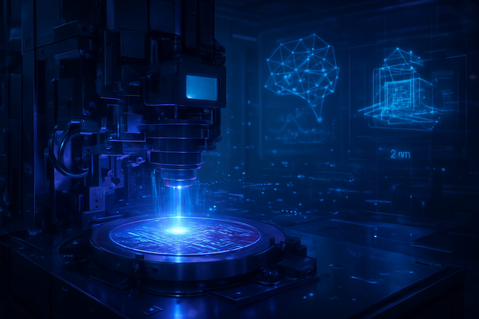
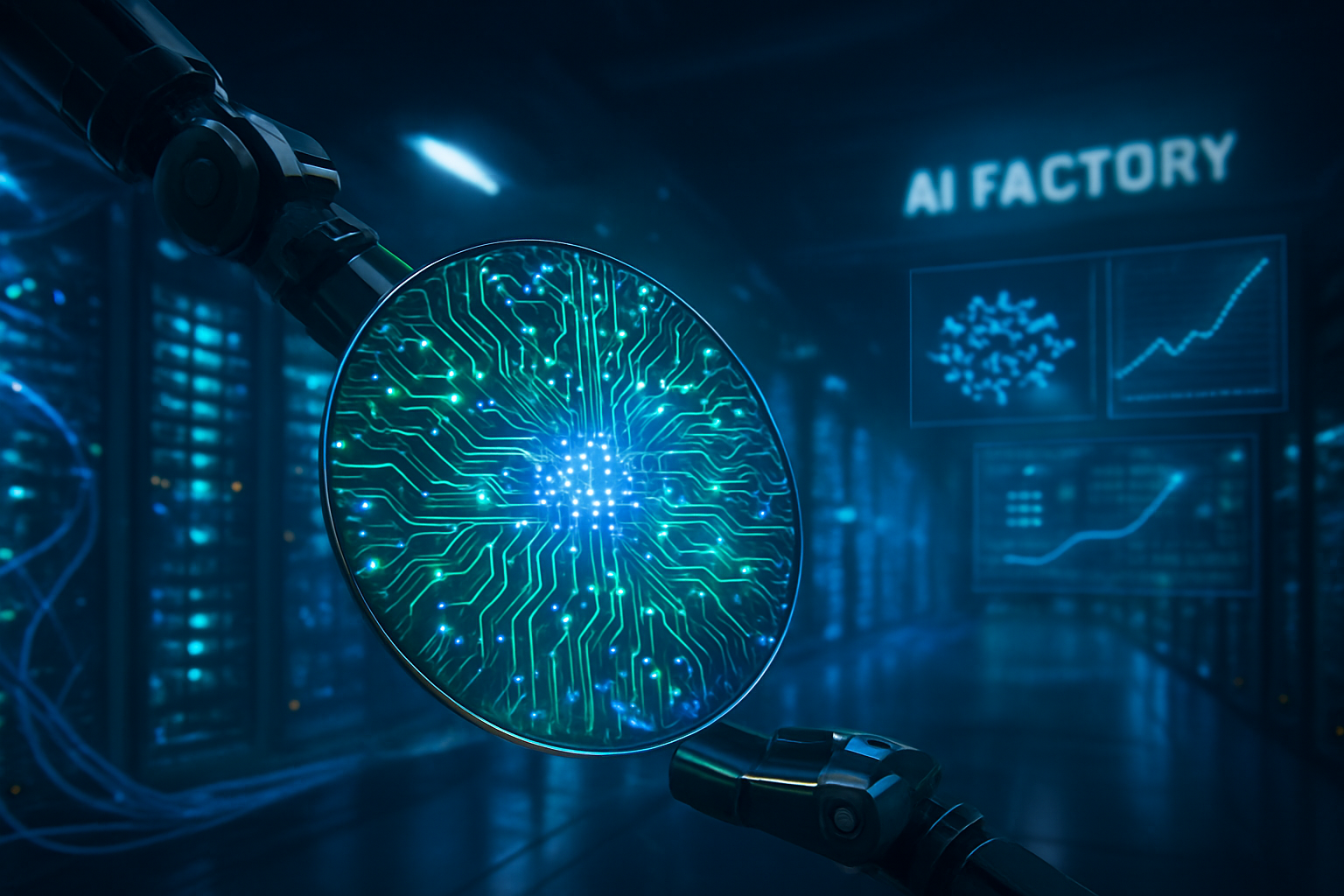
Engineering the Gigafab: A Technical Leap into the Angstrom Era
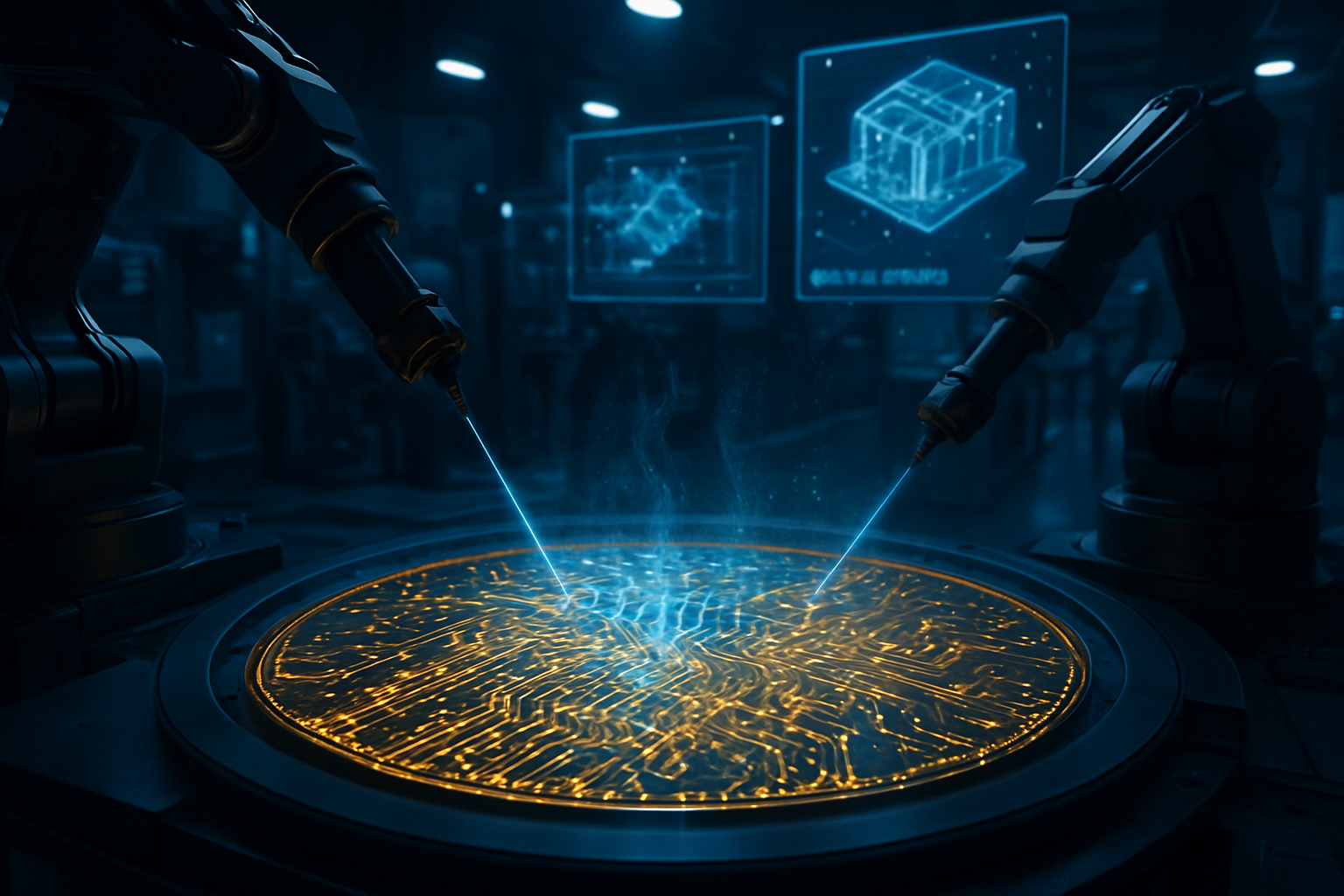
The technical specifications of the new Arizona cluster represent the bleeding edge of semiconductor physics. The 901-acre acquisition nearly doubles TSMC’s physical footprint in the region, providing the space necessary for "Gigafabs"—facilities capable of producing over 100,000 12-inch wafers per month. Unlike earlier iterations of the Arizona project which trailed Taiwan's "mother fabs" by several years, this new cluster is designed for "process parity." By 2027, the site will transition from 4nm and 3nm production to the highly anticipated 2nm (N2) node, featuring Gate-All-Around (GAAFET) transistor architecture.
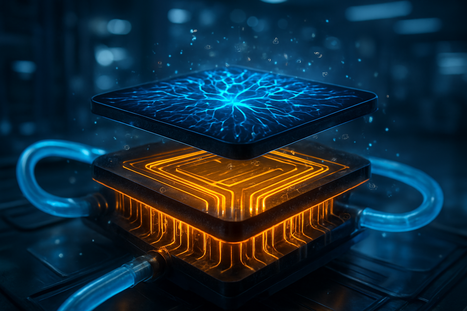
The most significant technical milestone, however, is the integration of the A16 (1.6nm) process node. Slated for the late 2020s in Arizona, the A16 node introduces Super Power Rail (SPR) technology. This breakthrough moves the power delivery network to the backside of the wafer, separate from the signal routing on the front. This architectural shift addresses the "power wall" that has hindered AI chip scaling, offering an estimated 10% increase in clock speeds and a 20% reduction in power consumption compared to the 2nm process.
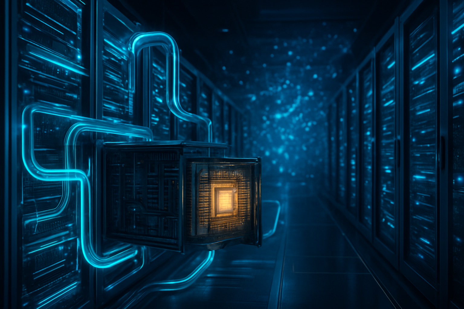
Industry experts note that this "independent cluster" strategy differs from previous approaches by including on-site advanced packaging facilities. Previously, wafers produced in the U.S. had to be shipped back to Asia for Chip-on-Wafer-on-Substrate (CoWoS) packaging. The new Arizona roadmap integrates these "back-end" processes directly into the Phoenix site, creating a closed-loop manufacturing ecosystem that slashes logistics lead times and protects sensitive IP from the risks of trans-Pacific transit.
The AI Titans Stake Their Claim: Apple, NVIDIA, and the New Market Dynamic
The expansion is a direct response to the insatiable demand from the "AI Titans." NVIDIA has emerged as a primary beneficiary, reportedly securing the lead customer position for the Arizona A16 capacity. This will support their upcoming "Feynman" GPU architecture, the successor to the Blackwell and Rubin series, which requires unprecedented transistor density to manage the trillions of parameters in future Large Language Models (LLMs). For NVIDIA, having a massive, reliable source of silicon on U.S. soil mitigates geopolitical risks and stabilizes its dominant market position in the data center sector.
Apple also remains a central figure in the Arizona strategy. The tech giant has already moved to secure over 50% of the initial 2nm capacity in the Phoenix cluster for its A-series and M-series chips. This ensures that the iPhone 18 and future MacBook Pros will be "Made in America" at the silicon level, a significant strategic advantage for Apple as it navigates global trade tensions and consumer demand for domestic manufacturing. The proximity of the fabs to Apple's design centers in the U.S. allows for tighter integration between hardware and software development.
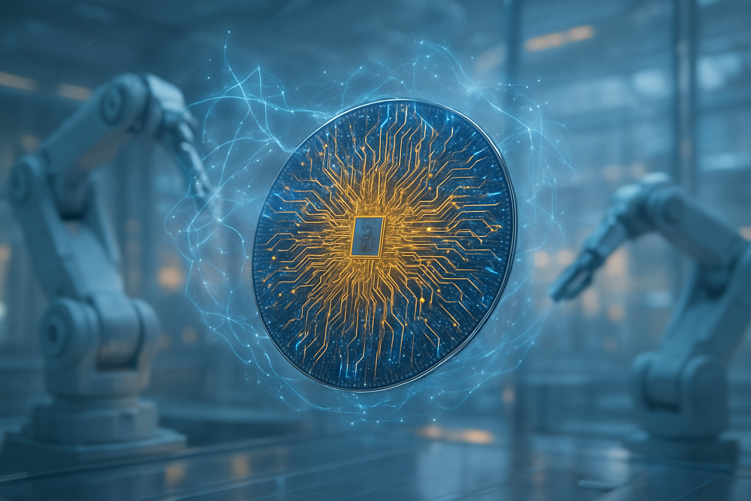
This $250 billion influx places immense pressure on competitors like Intel (NASDAQ:INTC) and Samsung (KRX:005930). While Intel has pursued a "Foundry 2.0" strategy with its own massive investments in Ohio and Arizona, TSMC's "Gigafab" scale and proven yield rates present a formidable challenge. For startups and mid-tier AI labs, the existence of a massive domestic foundry could lower the barriers to entry for custom silicon (ASICs), as TSMC looks to fill its dozen planned fabs with a diverse array of clients beyond just the trillion-dollar giants.
Geopolitical Resilience and the Global AI Landscape
The broader significance of the $250 billion trade deal cannot be overstated. By incentivizing TSMC to build 12 fabs in Arizona, the U.S. government is effectively creating a "silicon shield" that is geographical rather than purely political. This shift addresses the "single point of failure" concern that has haunted the tech industry for years: the concentration of 90% of advanced logic chips in a single, geopolitically sensitive island. The deal includes a 5% reduction in baseline tariffs for Taiwanese goods and massive credit guarantees, signaling a deep, long-term entanglement between the U.S. and Taiwan's economies.
However, the expansion is not without its critics and concerns. Environmental advocates point to the massive water and energy requirements of a 12-fab cluster in the arid Arizona desert. While TSMC has committed to near-100% water reclamation and the use of renewable energy, the sheer scale of the "Gigafab" cluster will test the state's infrastructure. Furthermore, the reliance on a single foreign entity for domestic AI sovereignty raises questions about long-term independence, even if the factories are physically located in Phoenix.
This milestone is frequently compared to the 1950s "Space Race," but with transistors instead of rockets. Just as the Apollo program spurred a generation of American innovation, the Arizona Gigafab cluster is expected to foster a local ecosystem of suppliers, researchers, and engineers. The "independent" nature of the site means that for the first time, the entire lifecycle of a chip—from design to wafer to packaging—can happen within a 50-mile radius in the United States.
The Road Ahead: Workforce, Water, and 1.6nm
Looking toward the late 2020s, the primary challenge for the Arizona expansion will be the human element. Managing a dozen fabs requires a workforce of tens of thousands of specialized engineers and technicians. TSMC has already begun partnering with local universities and technical colleges, but the "war for talent" between TSMC, Intel, and the surging AI startup sector remains a critical bottleneck. Near-term developments will likely focus on the completion of Fabs 4 through 6, with the first 2nm test runs expected by early 2027.
In the long term, we expect to see the Phoenix cluster move beyond traditional logic chips into specialized AI accelerators and photonics. As AI models move toward "physical world" applications like humanoid robotics and real-time edge processing, the low-latency benefits of domestic manufacturing will become even more pronounced. Experts predict that if the 12-fab goal is reached by 2030, Arizona will rival Taiwan’s Hsinchu Science Park as the most important plot of land in the digital world.
A New Chapter in Industrial History
The transformation of 901 acres of Arizona desert into a $250 billion silicon fortress marks a definitive chapter in the history of artificial intelligence. It is the moment when the "cloud" became grounded in physical, domestic infrastructure of an unprecedented scale. By moving its most advanced processes—2nm, A16, and beyond—to the United States, TSMC is not just building factories; it is anchoring the future of the AI economy to American soil.
As we look forward into 2026 and beyond, the success of this "independent gigafab cluster" will be measured not just in wafer starts, but in its ability to sustain the rapid pace of AI evolution. For investors, tech enthusiasts, and policymakers, the Phoenix complex is the place to watch. The chips that will define the next decade are being forged in the Arizona heat, and the stakes have never been higher.
This content is intended for informational purposes only and represents analysis of current AI developments.
TokenRing AI delivers enterprise-grade solutions for multi-agent AI workflow orchestration, AI-powered development tools, and seamless remote collaboration platforms.
For more information, visit https://www.tokenring.ai/.